 | –≠–ª–µ–∫—Ç—Ä–æ–Ω–Ω—ã–π –∫–æ–º–ø–æ–Ω–µ–Ω—Ç: 71V65803 | –°–∫–∞—á–∞—Ç—å:  PDF PDF  ZIP ZIP |

DECEMBER 2002
DSC-5304/05
1
©2002 Integrated Device Technology, Inc.
Pin Description Summary
Description
The IDT71V65603/5803 are 3.3V high-speed 9,437,184-bit
(9 Megabit) synchronous SRAMS. They are designed to eliminate dead bus
cycles when turning the bus around between reads and writes, or writes and
reads. Thus, they have been given the name ZBT
TM
, or Zero Bus Turnaround.
Features
x
x
x
x
x
256K x 36, 512K x 18 memory configurations
x
x
x
x
x
Supports high performance system speed - 150MHz
(3.8ns Clock-to-Data Access)
x
x
x
x
x
ZBT
TM
Feature - No dead cycles between write and read cycles
x
x
x
x
x
Internally synchronized output buffer enable eliminates the
need to control
OE
x
x
x
x
x
Single R/
W (READ/WRITE) control pin
x
x
x
x
x
Positive clock-edge triggered address, data, and control
signal registers for fully pipelined applications
x
x
x
x
x
4-word burst capability (interleaved or linear)
x
x
x
x
x
Individual byte write (
BW
1
-
BW
4
) control (May tie active)
x
x
x
x
x
Three chip enables for simple depth expansion
x
x
x
x
x
3.3V power supply (±5%)
x
x
x
x
x
3.3V I/O Supply (V
DDQ
)
x
x
x
x
x
Power down controlled by ZZ input
x
x
x
x
x
Packaged in a JEDEC standard 100-pin plastic thin quad
flatpack (TQFP), 119 ball grid array (BGA) and 165 fine pitch
ball grid array(fBGA).
A
0
-A
18
Address Inputs
Input
Synchronous
CE
1
, CE
2
,
CE
2
Chip Enables
Input
Synchronous
OE
Output Enable
Input
Asynchronous
R/
W
Read/Write Signal
Input
Synchronous
CEN
Clock Enable
Input
Synchronous
BW
1
,
BW
2
,
BW
3
,
BW
4
Individual Byte Write Selects
Input
Synchronous
CLK
Clock
Input
N/A
ADV/
LD
Advance burst address / Load new address
Input
Synchronous
LBO
Linear / Interleaved Burst Order
Input
Static
ZZ
Sleep Mode
Input
Asynchronous
I/O
0
-I/O
31
, I/O
P1
-I/O
P4
Data Input / Output
I/O
Synchronous
V
DD
, V
DDQ
Core Power, I/O Power
Supply
Static
V
SS
Ground
Supply
Static
5304 tbl 01
256K x 36, 512K x 18
3.3V Synchronous ZBTTM SRAMs
ZBTTM Feature
3.3V I/O, Burst Counter
Pipelined Outputs
IDT71V65603
IDT71V65803
Address and control signals are applied to the SRAM during one clock
cycle, and two cycles later the associated data cycle occurs, be it read or write.
The IDT71V65603/5803 contain data I/O, address and control signal
registers. Output enable is the only asynchronous signal and can be used
to disable the outputs at any given time.
A Clock Enable (
CEN) pin allows operation of the IDT71V65603/5803 to
be suspended as long as necessary. All synchronous inputs are ignored when
(
CEN) is high and the internal device registers will hold their previous values.
There are three chip enable pins (
CE1, CE2, CE2) that allow the user
to deselect the device when desired. If any one of these three are not asserted
when ADV/
LD is low, no new memory operation can be initiated. However,
any pending data transfers (reads or writes) will be completed. The data bus
will tri-state two cycles after chip is deselected or a write is initiated.
The IDT71V65603/5803 have an on-chip burst counter. In the burst
mode, the IDT71V65603/5803 can provide four cycles of data for a single
address presented to the SRAM. The order of the burst sequence is
defined by the
LBO input pin. The LBO pin selects between linear and
interleaved burst sequence. The ADV/
LD signal is used to load a new
external address (ADV/
LD = LOW) or increment the internal burst counter
(ADV/
LD = HIGH).
The IDT71V65603/5803 SRAM utilize IDT's latest high-performance
CMOS process, and are packaged in a JEDEC Standard 14mm x 20mm 100-
pin thin plastic quad flatpack (TQFP) as well as a 119 ball grid array (BGA) and
165 fine pitch ball grid array (fBGA) .
ZBT and Zero Bus Turnaround are trademarks of Integrated Device Technology, Inc. and the architecture is supported by Micron Technology and Motorola, Inc.

6.42
2
IDT71V65603, IDT71V65803, 256K x 36, 512K x 18, 3.3V Synchronous SRAMs with
ZBT
TM
TM
TM
TM
TM
Feature, 3.3V I/O, Burst Counter, and Pipelined Outputs Commercial and Industrial Temperature Ranges
Pin Definitions
(1)
NOTE:
1. All synchronous inputs must meet specified setup and hold times with respect to CLK.
Symbol
Pin Function
I/O
Active
Description
A
0
-A
18
Address Inputs
I
N/A
Synchronous Address inputs. The address register is trig gered by a combination of the
rising edge of CLK, ADV/
LD low, CEN low, and true chip enables.
ADV/
LD
Advance / Load
I
N/A
ADV/
LD is a synchronous input that is used to load the internal registers with new address
and control when it is sampled low at the rising edge of clock with the chip selected. When
ADV/
LD is low with the chip deselected, any burst in progress is terminated. When ADV/ LD
is sampled hig h then the internal burst counter is advanced for any burst that was in
progress. The external addresses are ignored when ADV/
LD is sampled high.
R/
W
Read / Write
I
N/A
R/
W signal is a synchronous input that identifies whether the current load cycle initiated is a
Read or Write access to the memory array. The data bus activity for the current cycle takes
place two clock cycles later.
CEN
Clock Enable
I
LOW
Synchronous Clock Enable Input. When
CEN is sampled high, all other synchronous
inputs, including clock are ignored and outputs re main unchanged. The effect of
CEN
sampled high on the device outp uts is as if the low to hig h clock transition did not occur.
For normal operation,
CEN must be sampled low at rising edge of clock.
BW
1
-
BW
4
Individual Byte
Write Enables
I
LOW
Synchro nous byte write enables. Each 9-bit byte has its own active low byte write enable.
On load write cycles (When R/
W and ADV/LD are sampled low) the appropriate byte write
signal (
BW
1
-
BW
4
) must be valid. The byte write signal must also be valid on each cycle of
a burst write. Byte Write signals are ignored when R/
W is sampled high. The appropriate
byte(s) of data are written into the device two cycles later.
BW
1
-
BW
4
can all be tied low if
always doing write to the entire 36-bit word.
CE
1
,
CE
2
Chip Enables
I
LOW
Synchronous active low chip enable.
CE
1
and
CE
2
are used with CE
2
to enable the
IDT71V65603/5803. (
CE
1
or
CE
2
sampled high or CE
2
sampled low) and ADV/
LD low at the
rising edge of clock, initiates a deselect cycle. The ZBT
TM
has a two cycle deselect, i.e.,
the data bus will tri-state two clock cycles after deselect is initiated.
CE
2
Chip Enable
I
HIGH
Synchrono us active high chip enable. CE
2
is used with
CE
1
and
CE
2
to enable the chip.
CE
2
has inverted po larity but otherwise identical to
CE
1
and
CE
2
.
CLK
Clock
I
N/A
This is the clock input to the IDT71V65603/5803. Except for
OE, all timing references for the
device are made with respect to the rising edge of CLK.
I/O
0
-I/O
31
I/O
P1
-I/O
P4
Data Input/Output
I/O
N/A
Synchro nous data input/output (I/O) pins. Both the data input path and data output path are
registered and triggered by the rising edge of CLK.
LBO
Linear Burst Order
I
LOW
Burst order selection input. When
LBO is high the Interleaved burst sequence is selected.
When
LBO is low the Linear burst sequence is selected. LBO is a static input and it must
not change during device operation.
OE
Output Enable
I
LOW
Asynchronous output enable.
OE must be low to read data from the 71V65603/5803. When
OE is high the I/O pins are in a high-impedance state. OE does not need to be actively
controlled for read and write cycles. In normal operation,
OE can be tied low.
ZZ
Sleep Mode
I
N/A
Asynchro nous sleep mode input. ZZ HIGH will gate the CLK internally and power down the
71V65603/5803 to its lowest p ower consumption level. Data retention is guaranteed in
Sleep Mode.
V
DD
Power Supply
N/A
N/A
3.3V core power supply.
V
DDQ
Power Supply
N/A
N/A
3.3V I/O Supply.
V
SS
Ground
N/A
N/A
Ground.
5304tbl 02
6.42
IDT71V65603, IDT71V65803, 256K x 36, 512K x 18, 3.3V Synchronous SRAMS with
ZBT
TM
TM
TM
TM
TM
Feature, 3.3V I/O, Burst Counter, and Pipelined Outputs Commercial and Industrial Temperature Ranges
3
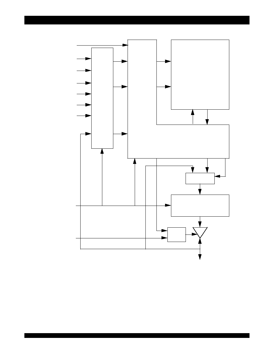
Functional Block Diagram
Clk
D
Q
D
Q
D
Q
Address A [0:17]
Control Logic
Address
Control
DI
DO
I
npu
t
R
e
g
is
te
r
5304 drw 01a
Clock
Data I/O [0:31],
I/O P[1:4]
D
Q
Cl
k
Output Register
Mux
Sel
Gate
OE
CE
1, CE2,
CE
2
R/
W
CEN
ADV/
LD
BW
x
LBO
256Kx36 BIT
MEMORY ARRAY
,

6.42
4
IDT71V65603, IDT71V65803, 256K x 36, 512K x 18, 3.3V Synchronous SRAMs with
ZBT
TM
TM
TM
TM
TM
Feature, 3.3V I/O, Burst Counter, and Pipelined Outputs Commercial and Industrial Temperature Ranges
Recommended DC Operating
Conditions
NOTES:
1. V
IL
(min.) = ≠1.0V for pulse width less than t
CYC
/2, once per cycle.
Functional Block Diagram
Symbol
Parameter
Min.
Typ.
Max.
Unit
V
DD
Core Supply Voltage
3.135
3.3
3.465
V
V
DDQ
I/O Supply Voltage
3.135
3.3
3.465
V
V
SS
Supply Voltage
0
0
0
V
V
IH
Input High Voltage - Inputs
2.0
____
V
DD
+0.3
V
V
IH
Input High Voltage - I/O
2.0
____
V
DDQ
+0.3
V
V
IL
Input Low Voltage
-0.3
(1)
____
0.8
V
5304 tbl 04
Clk
D
Q
D
Q
D
Q
Address A [0:18]
Control Logic
Address
Control
DI
DO
In
p
u
t
R
eg
i
s
t
e
r
5304 drw 01
Clock
Data I/O [0:15],
I/O P[1:2]
D
Q
Cl
k
Output Register
Mux
Sel
Gate
OE
CE
1, CE2,
CE
2
R/
W
CEN
ADV/
LD
BW
x
LBO
512x18 BIT
MEMORY ARRAY
,

6.42
IDT71V65603, IDT71V65803, 256K x 36, 512K x 18, 3.3V Synchronous SRAMS with
ZBT
TM
TM
TM
TM
TM
Feature, 3.3V I/O, Burst Counter, and Pipelined Outputs Commercial and Industrial Temperature Ranges
5
100 99 98 97 96 95 94 93 92 91 90
87 86 85 84 83 82 81
89 88
1
2
3
4
5
6
7
8
9
10
11
12
13
14
15
16
17
18
19
20
21
22
23
24
25
26
27
28
29
30
A
6
A
7
C
E
1
C
E
2
B
W
4
B
W
3
B
W
2
B
W
1
C
E
2
V
D
D
V
S
S
C
LK
R
/
W
C
E
N
O
E
A
D
V
/
LD
N
C
(2
)
A
17
A
8
A
9
31 32 33 34 35 36 37 38 39 40 41 42 43 44 45 46 47 48 49 50
D
N
U
(3
)
D
N
U
(3
)
D
N
U
(3
)
D
N
U
(3
)
LB
O
A
14
A
13
A
12
A
11
A
10
V
D
D
V
S
S
A
0
A
1
A
2
A
3
A
4
A
5
I/O
31
I/O
30
V
DDQ
V
SS
I/O
29
I/O
28
I/O
27
I/O
26
V
SS
V
DDQ
I/O
25
I/O
24
V
SS
V
DD
I/O
23
I/O
22
V
DDQ
V
SS
I/O
21
I/O
20
I/O
19
I/O
18
V
SS
V
DDQ
I/O
17
I/O
16
80
79
78
77
76
75
74
73
72
71
70
69
68
67
66
65
64
63
62
61
60
59
58
57
56
55
54
53
52
51
I/O
14
V
DDQ
V
SS
I/O
13
I/O
12
I/O
11
I/O
10
V
SS
V
DDQ
I/O
9
I/O
8
V
SS
V
DD
I/O
7
I/O
6
V
DDQ
V
SS
I/O
5
I/O
4
I/O
3
I/O
2
V
SS
V
DDQ
I/O
1
I/O
0
5304 drw 02
V
DD
(1)
I/O
15
I/O
P3
V
DD
(1)
I/O
P4
A
15
A
16
I/O
P1
V
DD
(1)
I/O
P2
ZZ
,
Recommended Operating
Temperature and Supply Voltage
Pin Configuration - 256K x 36
NOTES:
1. Pins 14, 16 and 66 do not have to be connected directly to VDD as long as the input voltage is
VIH.
2. Pin 84 is reserved for a future 16M.
3.
DNU=Do not use. Pins 38, 39, 42 and 43 are reserved for respective JTAG pins: TMS, TDI, TDO and TCK. The
current die revision allows these pins to be left unconnected, tied LOW (V
SS
), or tied HIGH (V
DD
).
Top View
100 TQFP
Grade
Temperature
(1)
V
SS
V
DD
V
DDQ
Commercial
0∞ C to +70∞ C
0V
3.3V±5%
3.3V±5%
Industrial
-40∞C to +85∞C
0V
3.3V±5%
3.3V±5%
5304 tbl 05
NOTES:
1.
T
A
is the "instant on" case temperature.

6.42
6
IDT71V65603, IDT71V65803, 256K x 36, 512K x 18, 3.3V Synchronous SRAMs with
ZBT
TM
TM
TM
TM
TM
Feature, 3.3V I/O, Burst Counter, and Pipelined Outputs Commercial and Industrial Temperature Ranges
Absolute Maximum Ratings
(1)
Pin Configuration - 512K x 18
119 BGA Capacitance
(1)
(T
A
= +25∞ C, f = 1.0MHz)
Top View
100 TQFP
NOTES:
1. Stresses greater than those listed under ABSOLUTE MAXIMUM RATINGS may
cause permanent damage to the device. This is a stress rating only and functional
operation of the device at these or any other conditions above those indicated
in the operational sections of this specification is not implied. Exposure to absolute
maximum rating conditions for extended periods may affect reliability.
2. V
DD
terminals only.
3. V
DDQ
terminals only.
4. Input terminals only.
5. I/O terminals only.
6. This is a steady-state DC parameter that applies after the power supply has
reached its nominal operating value. Power sequencing is not necessary;
however, the voltage on any input or I/O pin cannot exceed V
DDQ
during power
supply ramp up.
7. T
A
is the "instant on" case temperature.
NOTE:
1. This parameter is guaranteed by device characterization, but not production tested.
Symbol
Rating
Commercial &
Industrial
Unit
V
TERM
(2)
Terminal Voltage with
Respect to GND
-0.5 to +4.6
V
V
TERM
(3,6)
Terminal Voltage with
Respect to GND
-0.5 to V
DD
V
V
TERM
(4,6)
Terminal Voltage with
Respect to GND
-0.5 to V
DD
+0.5
V
V
TERM
(5,6)
Terminal Voltage with
Respect to GND
-0.5 to V
DDQ
+0.5
V
T
A
(7)
Commercial
Operating Temperature
-0 to +70
o
C
Industrial
Operating Temperature
-40 to +85
o
C
T
BIAS
Temperature
Under Bias
-55 to +125
o
C
T
STG
Storage
Temperature
-55 to +125
o
C
P
T
Power Dissipation
2.0
W
I
OUT
DC Output Current
50
mA
5304 tbl 06
Symbol
Parameter
(1)
Conditions
Max.
Unit
C
IN
Input Capacitance
V
IN
= 3dV
5
pF
C
I/O
I/O Capacitance
V
OUT
= 3dV
7
pF
5304 tbl 07
100 99 98 97 96 95 94 93 92 91 90
87 86 85 84 83 82 81
89 88
1
2
3
4
5
6
7
8
9
10
11
12
13
14
15
16
17
18
19
20
21
22
23
24
25
26
27
28
29
30
A
6
A
7
C
E
1
C
E
2
N
C
N
C
B
W
2
B
W
1
C
E
2
V
D
D
V
S
S
C
LK
R
/
W
C
E
N
O
E
A
D
V
/
LD
N
C
(2
)
A
18
A
8
A
9
31 32 33 34 35 36 37 38 39 40 41 42 43 44 45 46 47 48 49 50
D
N
U
(3
)
D
N
U
(3
)
D
N
U
(3
)
D
N
U
(3
)
LB
O
A
15
A
14
A
13
A
12
A
11
V
D
D
V
S
S
A
0
A
1
A
2
A
3
A
4
A
5
NC
NC
V
DDQ
V
SS
NC
I/O
P2
I/O
15
I/O
14
V
SS
V
DDQ
I/O
13
I/O
12
V
SS
V
DD
I/O
11
I/O
10
V
DDQ
V
SS
I/O
9
I/O
8
NC
NC
V
SS
V
DDQ
NC
NC
80
79
78
77
76
75
74
73
72
71
70
69
68
67
66
65
64
63
62
61
60
59
58
57
56
55
54
53
52
51
NC
V
DDQ
V
SS
NC
I/O
P1
I/O
7
I/O
6
V
SS
V
DDQ
I/O
5
I/O
4
V
SS
V
DD
I/O
3
I/O
2
V
DDQ
V
SS
I/O
1
I/O
0
NC
NC
V
SS
V
DDQ
NC
NC
5304 drw 02a
V
DD
(1)
NC
NC
V
DD
(1)
NC
A
16
A
17
NC
V
DD
(1)
A
10
ZZ
,
NOTES:
1. Pins 14, 16 and 66 do not have to be connected directly to V
DD
as long as
the input voltage is
V
IH
.
2. Pin 84 is reserved for a future 16M.
3. DNU=Do not use. Pins 38, 39, 42 and 43 are reserved for respective
JTAG pins: TMS, TDI, TDO and TCK. The current die revision allows
these pins to be left unconnected, tied LOW (V
SS
), or tied HIGH (V
DD
).
Symbol
Parameter
(1)
Conditions
Max.
Unit
C
IN
Input Capacitance
V
IN
= 3dV
7
pF
C
I/O
I/O Capacitance
V
OUT
= 3dV
7
pF
5304 tbl 07a
100 TQFP Capacitance
(1)
(T
A
= +25∞ C, f = 1.0MHz)
Symbol
Parameter
(1)
Conditions
Max.
Unit
C
IN
Input Capacitance
V
IN
= 3dV
TBD
pF
C
I/O
I/O Capacitance
V
OUT
= 3dV
TBD
pF
5304 tbl 07b
165 fBGA Capacitance
(1)
(T
A
= +25∞ C, f = 1.0MHz)

6.42
IDT71V65603, IDT71V65803, 256K x 36, 512K x 18, 3.3V Synchronous SRAMS with
ZBT
TM
TM
TM
TM
TM
Feature, 3.3V I/O, Burst Counter, and Pipelined Outputs Commercial and Industrial Temperature Ranges
7
NOTES:
1. J3, J5, and R5 do not have to be directly connected to V
DD
as long as the input voltage is
V
IH
.
2. A4 is reserved for future 16M.
3. DNU = Do not use. Pin U2, U3, U4, U5 and U6 are reserved for respective JTAG pins: TMS, TDI, TCK, TDO and
TRST. The current die revision allows
these pins to be left unconnected, tied LOW (V
SS
), or tied HIGH (V
DD
).
Pin Configuration - 256K X 36, 119 BGA
Top View
Pin Configuration - 512K X 18, 119 BGA
Top View
1
2
3
4
5
6
7
A
V
DDQ
A
6
A
4
A
8
A
16
V
DDQ
B
NC
CE
2
A
3
ADV/
LD
A
9
CE
2
NC
C
A
7
A
2
V
DD
A
12
A
15
NC
D
I/O
16
I/O
P3
V
SS
NC
V
SS
I/O
P2
I/O
15
E
I/O
17
I/O
18
V
SS
V
SS
I/O
13
I/O
14
F
V
DDQ
I/O
19
V
SS
OE
V
SS
I/O
12
V
DDQ
G
I/O
20
I/O
21
BW
3
BW
2
I/O
11
I/O
10
H
I/O
22
I/O
23
V
SS
R/
W
V
SS
I/O
9
I/O
8
J
V
DDQ
V
DD
V
DD
V
DD
V
DDQ
K
I/O
24
I/O
26
V
SS
CLK
V
SS
I/O
6
I/O
7
L
I/O
25
I/O
27
BW
4
NC
BW
1
I/O
4
I/O
5
M
V
DDQ
I/O
28
V
SS
CEN
V
SS
I/O
3
V
DDQ
N
I/O
29
I/O
30
V
SS
A
1
V
SS
I/O
2
I/O
1
P
I/O
31
I/O
P4
V
SS
A
0
V
SS
I/O
0
I/O
P1
R
NC
A
5
LBO
V
DD
A
13
T
NC
NC
A
10
A
11
A
14
NC
ZZ
U
V
DDQ
DNU
(3)
DNU
(3)
DNU
(3)
V
DDQ
5304 drw 13A
V
DD(1)
NC
NC
(2)
CE
1
A17
V
DD(1)
V
DD(1)
,
DNU
(3)
DNU
(3)
NC
1
2
3
4
5
6
7
A
V
DDQ
A
6
A
4
NC(2)
A
8
A
16
V
DDQ
B
NC
CE2
A
3
ADV/
LD
A
9
CE
2
NC
C
A
7
A
2
V
DD
A
13
A
17
NC
D
I/O
8
NC
V
SS
NC
V
SS
I/O
7
NC
E
NC
I/O
9
V
SS
V
SS
NC
I/O
6
F
V
DDQ
NC
V
SS
OE
V
SS
I/O
5
V
DDQ
G
NC
I/O
10
BW
2
NC
I/O
4
H
I/O
11
NC
V
SS
R/
W
V
SS
I/O
3
NC
J
V
DDQ
V
DD
V
DD
V
DD
V
DDQ
K
NC
I/O
12
V
SS
CLK
V
SS
NC
I/O
2
L
I/O
13
NC
NC
BW
1
I/O
1
NC
M
V
DDQ
I/O
14
V
SS
CEN
V
SS
NC
V
DDQ
N
I/O
15
NC
V
SS
A
1
V
SS
I/O
0
NC
P
NC
I/O
P2
V
SS
A
0
V
SS
NC
I/O
P1
R
NC
A
5
LBO
V
DD
A
12
T
NC
A
10
A
15
NC
A
14
A
11
ZZ
U
V
DDQ
DNU
(3)
DNU
(3)
DNU
(3)
DNU
(3)
NC
V
DDQ
5304 drw 13B
NC
DD(1)
V
DNU
(3)
V
SS
V
SS
CE
1
A18
V
DD(1)
V
DD(1)

6.42
8
IDT71V65603, IDT71V65803, 256K x 36, 512K x 18, 3.3V Synchronous SRAMs with
ZBT
TM
TM
TM
TM
TM
Feature, 3.3V I/O, Burst Counter, and Pipelined Outputs Commercial and Industrial Temperature Ranges
NOTES:
1. H1, H2, and N7 do not have to be directly connected to V
DD
as long as the input voltage is
V
IH
.
2. B9, B11, A1, R2 and P2 is reserved for future 18M, 36M, 72M, 144M and 288M, respectively.
3. DNU=Do not use. Pins P5, R5, P7 and R7 are reserved for respective JTAG pins: TDI, TMS, TDO and TCK on future revisions. The current die revision
allows these pins to be left unconnected, tied LOW (V
SS
), or tied HIGH (V
DD
).
Pin Configuration - 256K X 36, 165 fBGA
Pin Configuration - 512K X 18, 165 fBGA
1
2
3
4
5
6
7
8
9
10
11
A
NC
(2)
A
7
CE
1
BW
3
BW
2
CE
2
CEN
ADV
/LD
A
17
A
8
NC
B
NC
A
6
CE
2
BW
4
BW
1
CLK
R/
W
OE
NC
(2)
A
9
NC
(2)
C
I/O
P3
NC
V
DDQ
V
SS
V
SS
V
SS
V
SS
V
SS
V
DDQ
NC
I/O
P2
D
I/O
17
I/O
16
V
DDQ
V
DD
V
SS
V
SS
V
SS
V
DD
V
DDQ
I/O
15
I/O
14
E
I/O
19
I/O
18
V
DDQ
V
DD
V
SS
V
SS
V
SS
V
DD
V
DDQ
I/O
13
I/O
12
F
I/O
21
I/O
20
V
DDQ
V
DD
V
SS
V
SS
V
SS
V
DD
V
DDQ
I/O
11
I/O
10
G
I/O
23
I/O
22
V
DDQ
V
DD
V
SS
V
SS
V
SS
V
DD
V
DDQ
I/O
9
I/O
8
H
V
DD
(1)
V
DD
(1)
NC
V
DD
V
SS
V
SS
V
SS
V
DD
NC
NC
ZZ
J
I/O
25
I/O
24
V
DDQ
V
DD
V
SS
V
SS
V
SS
V
DD
V
DDQ
I/O
7
I/O
6
K
I/O
27
I/O
26
V
DDQ
V
DD
V
SS
V
SS
V
SS
V
DD
V
DDQ
I/O
5
I/O
4
L
I/O
29
I/O
28
V
DDQ
V
DD
V
SS
V
SS
V
SS
V
DD
V
DDQ
I/O
3
I/O
2
M
I/O
31
I/O
30
V
DDQ
V
DD
V
SS
V
SS
V
SS
V
DD
V
DDQ
I/O
1
I/O
0
N
I/O
P4
NC
V
DDQ
V
SS
DNU
(3)
NC
V
DD
(1)
V
SS
V
DDQ
NC
I/O
P1
P
NC
NC
(2)
A
5
A
2
DNU
(3)
A
1
DNU
(3)
A
10
A
13
A
14
NC
R
LBO
NC
(2)
A
4
A
3
DNU
(3)
A
0
DNU
(3)
A
11
A
12
A
15
A
16
5304 tbl 25a
1
2
3
4
5
6
7
8
9
10
11
A
NC
(2)
A
7
CE
1
BW
2
NC
CE
2
CEN
ADV
/LD
A
18
A
8
A
10
B
NC
A
6
CE
2
NC
BW
1
CLK
R/
W
OE
NC
(2)
A
9
NC
(2)
C
NC
NC
V
DDQ
V
SS
V
SS
V
SS
V
SS
V
SS
V
DDQ
NC
I/O
P1
D
NC
I/O
8
V
DDQ
V
DD
V
SS
V
SS
V
SS
V
DD
V
DDQ
NC
I/O
7
E
NC
I/O
9
V
DDQ
V
DD
V
SS
V
SS
V
SS
V
DD
V
DDQ
NC
I/O
6
F
NC
I/O
10
V
DDQ
V
DD
V
SS
V
SS
V
SS
V
DD
V
DDQ
NC
I/O
5
G
NC
I/O
11
V
DDQ
V
DD
V
SS
V
SS
V
SS
V
DD
V
DDQ
NC
I/O
4
H
V
DD
(1)
V
DD
(1)
NC
V
DD
V
SS
V
SS
V
SS
V
DD
NC
NC
ZZ
J
I/O
12
NC
V
DDQ
V
DD
V
SS
V
SS
V
SS
V
DD
V
DDQ
I/O
3
NC
K
I/O
13
NC
V
DDQ
V
DD
V
SS
V
SS
V
SS
V
DD
V
DDQ
I/O
2
NC
L
I/O
14
NC
V
DDQ
V
DD
V
SS
V
SS
V
SS
V
DD
V
DDQ
I/O
1
NC
M
I/O
15
NC
V
DDQ
V
DD
V
SS
V
SS
V
SS
V
DD
V
DDQ
I/O
0
NC
N
I/O
P2
NC
V
DDQ
V
SS
DNU
(3)
NC
V
DD
(1)
V
SS
V
DDQ
NC
NC
P
NC
NC
(2)
A
5
A
2
DNU
(3)
A
1
DNU
(3)
A
11
A
14
A
15
NC
R
LBO
NC
(2)
A
4
A
3
DNU
(3)
A
0
DNU
(3)
A
12
A
13
A
16
A
17
5304 tbl25b

6.42
IDT71V65603, IDT71V65803, 256K x 36, 512K x 18, 3.3V Synchronous SRAMS with
ZBT
TM
TM
TM
TM
TM
Feature, 3.3V I/O, Burst Counter, and Pipelined Outputs Commercial and Industrial Temperature Ranges
9
Synchronous Truth Table
(1)
Partial Truth Table for Writes
(1)
NOTES:
1. L = V
IL
, H = V
IH
, X = Don't Care.
2. When ADV/
LD signal is sampled high, the internal burst counter is incremented. The R/W signal is ignored when the counter is advanced. Therefore the nature of
the burst cycle (Read or Write) is determined by the status of the R/
W signal when the first address is loaded at the beginning of the burst cycle.
3. Deselect cycle is initiated when either (
CE
1
, or
CE
2
is sampled high or CE
2
is sampled low) and ADV/
LD is sampled low at rising edge of clock. The data bus will
tri-state two cycles after deselect is initiated.
4. When
CEN is sampled high at the rising edge of clock, that clock edge is blocked from propogating through the part. The state of all the internal registers and the I/
Os remains unchanged.
5. To select the chip requires
CE
1
= L,
CE
2
= L, CE
2
= H on these chip enables. Chip is deselected if any one of the chip enables is false.
6. Device Outputs are ensured to be in High-Z after the first rising edge of clock upon power-up.
7. Q - Data read from the device, D - data written to the device.
NOTES:
1. L = V
IL
, H = V
IH
, X = Don't Care.
2. Multiple bytes may be selected during the same cycle.
3. N/A for X18 configuration.
CEN
R/
W
Chip
(5)
Enable
ADV/
LD
BWx
ADDRESS
USED
PREVIOUS CYCLE
CURRENT CYCLE
I/O
(2 cycles later)
L
L
Select
L
Valid
External
X
LOAD WRITE
D
(7)
L
H
Select
L
X
External
X
LOAD READ
Q
(7)
L
X
X
H
Valid
Internal
LOAD WRITE /
BURST WRITE
BURST WRITE
(Advance burst counter)
(2)
D
(7)
L
X
X
H
X
Internal
LOAD READ /
BURST READ
BURST READ
(Advance burst counter)
(2)
Q
(7)
L
X
Deselect
L
X
X
X
DESELECT or STOP
(3)
HiZ
L
X
X
H
X
X
DESELECT / NOOP
NOOP
HiZ
H
X
X
X
X
X
X
SUSPEND
(4)
Previous Value
5304 tbl 08
OPERATION
R/
W
BW
1
BW
2
BW
3
(3)
BW
4
(3)
READ
H
X
X
X
X
WRITE ALL BYTES
L
L
L
L
L
WRITE BYTE 1 (I/O[0:7], I/O
P1
)
(2)
L
L
H
H
H
WRITE BYTE 2 (I/O[8:15], I/O
P2
)
(2)
L
H
L
H
H
WRITE BYTE 3 (I/O[16:23], I/O
P3
)
(2,3)
L
H
H
L
H
WRITE BYTE 4 (I/O[24:31], I/O
P4
)
(2,3)
L
H
H
H
L
NO WRITE
L
H
H
H
H
5304 tbl 09

6.42
10
IDT71V65603, IDT71V65803, 256K x 36, 512K x 18, 3.3V Synchronous SRAMs with
ZBT
TM
TM
TM
TM
TM
Feature, 3.3V I/O, Burst Counter, and Pipelined Outputs Commercial and Industrial Temperature Ranges
Linear Burst Sequence Table (LBO=V
SS
)
Interleaved Burst Sequence Table (LBO=V
DD
)
Functional Timing Diagram
(1)
NOTES:
1. This assumes
CEN, CE
1
, CE
2
,
CE
2
are all true.
2. All Address, Control and Data_In are only required to meet set-up and hold time with respect to the rising edge of clock. Data_Out is valid after a clock-to-data
delay from the rising edge of clock.
NOTE:
1. Upon completion of the Burst sequence the counter wraps around to its initial state and continues counting.
NOTE:
1. Upon completion of the Burst sequence the counter wraps around to its initial state and continues counting.
Sequence 1
Sequence 2
Sequence 3
Sequence 4
A1
A0
A1
A0
A1
A0
A1
A0
First Address
0
0
0
1
1
0
1
1
Second Address
0
1
0
0
1
1
1
0
Third Address
1
0
1
1
0
0
0
1
Fourth Address
(1)
1
1
1
0
0
1
0
0
5304 tbl 10
Sequence 1
Sequence 2
Sequence 3
Sequence 4
A1
A0
A1
A0
A1
A0
A1
A0
First Address
0
0
0
1
1
0
1
1
Second Address
0
1
1
0
1
1
0
0
Third Address
1
0
1
1
0
0
0
1
Fourth Address
(1)
1
1
0
0
0
1
1
0
5304 tbl 11
n+29
A29
C29
D/Q27
ADDRESS
(2)
(A0 - A17)
CONTROL
(2)
(R/
W
, ADV/
LD
,
BW
x)
DATA
(2)
I/O [0:31], I/O P[1:4]
CYCLE
CLOCK
n+30
A30
C30
D/Q28
n+31
A31
C31
D/Q29
n+32
A32
C32
D/Q30
n+33
A33
C33
D/Q31
n+34
A34
C34
D/Q32
n+35
A35
C35
D/Q33
n+36
A36
C36
D/Q34
n+37
A37
C37
D/Q35
5304 drw 03
,

6.42
IDT71V65603, IDT71V65803, 256K x 36, 512K x 18, 3.3V Synchronous SRAMS with
ZBT
TM
TM
TM
TM
TM
Feature, 3.3V I/O, Burst Counter, and Pipelined Outputs Commercial and Industrial Temperature Ranges
11
NOTES:
1. H = High; L = Low; X = Don't Care; Z = High Impedance.
2.
CE = L is defined as CE
1
= L,
CE
2
= L and CE
2
= H.
CE = H is defined as CE
1
= H,
CE
2
= H or CE
2
= L.
Read Operation
(1)
Device Operation - Showing Mixed Load, Burst,
Deselect and NOOP Cycles
(2)
NOTES:
1.
CE = L is defined as CE
1
= L,
CE
2
= L and CE
2
= H.
CE = H is defined as CE
1
= H,
CE
2
= H or CE
2
= L.
2. H = High; L = Low; X = Don't Care; Z = High Impedance.
Cycle
Address
R/
W
ADV/
LD
CE
(1)
CEN
BWx
OE
I/O
Comments
n
A
0
H
L
L
L
X
X
X
Load read
n+1
X
X
H
X
L
X
X
X
Burst read
n+2
A
1
H
L
L
L
X
L
Q
0
Load read
n+3
X
X
L
H
L
X
L
Q
0+1
Deselect or STOP
n+4
X
X
H
X
L
X
L
Q
1
NOOP
n+5
A
2
H
L
L
L
X
X
Z
Load read
n+6
X
X
H
X
L
X
X
Z
Burst read
n+7
X
X
L
H
L
X
L
Q
2
Deselect or STOP
n+8
A
3
L
L
L
L
L
L
Q
2+1
Load write
n+9
X
X
H
X
L
L
X
Z
Burst write
n+10
A
4
L
L
L
L
L
X
D
3
Load write
n+11
X
X
L
H
L
X
X
D
3+1
Deselect or STOP
n+12
X
X
H
X
L
X
X
D
4
NOOP
n+13
A
5
L
L
L
L
L
X
Z
Load write
n+14
A
6
H
L
L
L
X
X
Z
Load read
n+15
A
7
L
L
L
L
L
X
D
5
Load write
n+16
X
X
H
X
L
L
L
Q
6
Burst write
n+17
A
8
H
L
L
L
X
X
D
7
Load read
n+18
X
X
H
X
L
X
X
D
7+1
Burst read
n+19
A
9
L
L
L
L
L
L
Q
8
Load write
5304tbl 12
Cycle
Address
R/
W
ADV/
LD
CE
(2)
CEN
BWx
OE
I/O
Comments
n
A
0
H
L
L
L
X
X
X
Address and Control meet setup
n+1
X
X
X
X
L
X
X
X
Clock Setup Valid
n+2
X
X
X
X
X
X
L
Q
0
Contents of Address A
0
Read Out
5304 tbl 13

6.42
12
IDT71V65603, IDT71V65803, 256K x 36, 512K x 18, 3.3V Synchronous SRAMs with
ZBT
TM
TM
TM
TM
TM
Feature, 3.3V I/O, Burst Counter, and Pipelined Outputs Commercial and Industrial Temperature Ranges
Burst Write Operation
(1)
Burst Read Operation
(1)
Write Operation
(1)
NOTES:
1. H = High; L = Low; X = Don't Care; Z = High Impedance..
2.
CE = L is defined as CE
1
= L,
CE
2
= L and CE
2
= H.
CE = H is defined as CE
1
= H,
CE
2
= H or CE
2
= L.
NOTES:
1. H = High; L = Low; X = Don't Care; Z = High Impedance.
2.
CE = L is defined as CE
1
= L,
CE
2
= L and CE
2
= H.
CE = H is defined as CE
1
= H,
CE
2
= H or CE
2
= L.
NOTES:
1. H = High; L = Low; X = Don't Care; ? = Don't Know; Z = High Impedance.
2.
CE = L is defined as CE
1
= L,
CE
2
= L and CE
2
= H.
CE = H is defined as CE
1
= H,
CE
2
= H or CE
2
= L.
Cycle
Address
R/
W
ADV/
LD
CE
(2)
CEN
BWx
OE
I/O
Comments
n
A
0
H
L
L
L
X
X
X
Address and Control meet setup
n+1
X
X
H
X
L
X
X
X
Clock Setup Valid, Advance Counter
n+2
X
X
H
X
L
X
L
Q
0
Address A
0
Read Out, Inc. Count
n+3
X
X
H
X
L
X
L
Q
0+1
Address A
0+1
Read Out, Inc. Count
n+4
X
X
H
X
L
X
L
Q
0+2
Address A
0+2
Read Out, Inc. Count
n+5
A
1
H
L
L
L
X
L
Q
0+3
Address A
0+3
Read Out, Load A
1
n+6
X
X
H
X
L
X
L
Q
0
Address A
0
Read Out, Inc. Count
n+7
X
X
H
X
L
X
L
Q
1
Address A
1
Read Out, Inc. Count
n+8
A
2
H
L
L
L
X
L
Q
1+1
Address A
1+1
Read Out, Load A
2
5304 tbl 14
Cycle
Address
R/
W
ADV/
LD
CE
(2)
CEN
BWx
OE
I/O
Comments
n
A
0
L
L
L
L
L
X
X
Address and Control meet setup
n+1
X
X
X
X
L
X
X
X
Clock Setup Valid
n+2
X
X
X
X
L
X
X
D
0
Write to Address A
0
5304 tbl 15
Cycle
Address
R/
W
ADV/
LD
CE
(2)
CEN
BWx
OE
I/O
Comments
n
A
0
L
L
L
L
L
X
X
Address and Control meet setup
n+1
X
X
H
X
L
L
X
X
Clock Setup Valid, Inc. Count
n+2
X
X
H
X
L
L
X
D
0
Address A
0
Write, Inc. Count
n+3
X
X
H
X
L
L
X
D
0+1
Address A
0+1
Write, Inc. Count
n+4
X
X
H
X
L
L
X
D
0+2
Address A
0+2
Write, Inc. Count
n+5
A
1
L
L
L
L
L
X
D
0+3
Address A
0+3
Write, Load A
1
n+6
X
X
H
X
L
L
X
D
0
Address A
0
Write, Inc. Count
n+7
X
X
H
X
L
L
X
D
1
Address A
1
Write, Inc. Count
n+8
A
2
L
L
L
L
L
X
D
1+1
Address A
1+1
Write, Load A
2
5304 tbl 16

6.42
IDT71V65603, IDT71V65803, 256K x 36, 512K x 18, 3.3V Synchronous SRAMS with
ZBT
TM
TM
TM
TM
TM
Feature, 3.3V I/O, Burst Counter, and Pipelined Outputs Commercial and Industrial Temperature Ranges
13
Read Operation with Clock Enable Used
(1)
Write Operation with Clock Enable Used
(1)
NOTES:
1. H = High; L = Low; X = Don't Care; Z = High Impedance.
2.
CE = L is defined as CE
1
= L,
CE
2
= L and CE
2
= H.
CE = H is defined as CE
1
= H,
CE
2
= H or CE
2
= L.
NOTES:
1. H = High; L = Low; X = Don't Care; Z = High Impedance.
2.
CE = L is defined as CE
1
= L,
CE
2
= L and CE
2
= H.
CE = H is defined as CE
1
= H,
CE
2
= H or CE
2
= L.
Cycle
Address
R/
W
ADV/
LD
CE
(2)
CEN
BWx
OE
I/O
Comments
n
A
0
H
L
L
L
X
X
X
Address and Control meet setup
n+1
X
X
X
X
H
X
X
X
Clock n+1 Ignored
n+2
A
1
H
L
L
L
X
X
X
Clock Valid
n+3
X
X
X
X
H
X
L
Q
0
Clock Ignored, Data Q
0
is on the bus.
n+4
X
X
X
X
H
X
L
Q
0
Clock Ignored, Data Q
0
is on the bus.
n+5
A
2
H
L
L
L
X
L
Q
0
Address A
0
Read out (bus trans.)
n+6
A
3
H
L
L
L
X
L
Q
1
Address A
1
Read out (bus trans.)
n+7
A
4
H
L
L
L
X
L
Q
2
Ad dress A2 Read out (bus trans.)
5304 tbl 17
Cycle
Address
R/
W
ADV
/LD
CE
(2)
CEN
BWx
OE
I/O
Comments
n
A
0
L
L
L
L
L
X
X
Address and Control meet setup.
n+1
X
X
X
X
H
X
X
X
Clock n+1 Ignored.
n+2
A
1
L
L
L
L
L
X
X
Clock Valid.
n+3
X
X
X
X
H
X
X
X
Clock Ignored.
n+4
X
X
X
X
H
X
X
X
Clock Ignored.
n+5
A
2
L
L
L
L
L
X
D
0
Write Data D
0
n+6
A
3
L
L
L
L
L
X
D
1
Write Data D
1
n+7
A
4
L
L
L
L
L
X
D
2
Write Data D
2
5304 tbl 18
6.42
14
IDT71V65603, IDT71V65803, 256K x 36, 512K x 18, 3.3V Synchronous SRAMs with
ZBT
TM
TM
TM
TM
TM
Feature, 3.3V I/O, Burst Counter, and Pipelined Outputs Commercial and Industrial Temperature Ranges
NOTES:
1. H = High; L = Low; X = Don't Care; ? = Don't Know; Z = High Impedance.
2.
CE = L is defined as CE
1
= L,
CE
2
= L and CE
2
= H.
CE = H is defined as CE
1
= H,
CE
2
= H or CE
2
= L.
3. Device Outputs are ensured to be in High-Z after the first rising edge of clock upon power-up.
Read Operation with Chip Enable Used
(1)
Write Operation with Chip Enable Used
(1)
NOTES:
1. H = High; L = Low; X = Don't Care; ? = Don't Know; Z = High Impedance.
2.
CE = L is defined as CE
1
= L,
CE
2
= L and CE
2
= H.
CE = H is defined as CE
1
= H,
CE
2
= H or CE
2
= L.
Cycle
Address
R/
W
ADV/
LD
CE
(2)
CEN
BWx
OE
I/O
(3)
Comments
n
X
X
L
H
L
X
X
?
Deselected.
n+1
X
X
L
H
L
X
X
?
Deselected.
n+2
A
0
H
L
L
L
X
X
Z
Address and Control meet setup
n+3
X
X
L
H
L
X
X
Z
Deselected or STOP.
n+4
A
1
H
L
L
L
X
L
Q
0
Address A
0
Read out. Load A
1
.
n+5
X
X
L
H
L
X
X
Z
Deselected or STOP.
n+6
X
X
L
H
L
X
L
Q
1
Address A
1
Read out. Deselected.
n+7
A
2
H
L
L
L
X
X
Z
Address and control meet setup.
n+8
X
X
L
H
L
X
X
Z
Deselected or STOP.
n+9
X
X
L
H
L
X
L
Q
2
Address A
2
Read out. Deselected.
5304 tbl 19
Cycle
Address
R
/W
ADV/
LD
CE
(2)
CEN
BWx
OE
I/O
(3)
Comments
n
X
X
L
H
L
X
X
?
Deselected.
n+1
X
X
L
H
L
X
X
?
Deselected.
n+2
A
0
L
L
L
L
L
X
Z
Address and Control meet setup
n+3
X
X
L
H
L
X
X
Z
Deselected or STOP.
n+4
A
1
L
L
L
L
L
X
D
0
Address D
0
Write in. Load A
1
.
n+5
X
X
L
H
L
X
X
Z
Deselected or STOP.
n+6
X
X
L
H
L
X
X
D
1
Address D
1
Write in. Deselected.
n+7
A
2
L
L
L
L
L
X
Z
Address and control meet setup.
n+8
X
X
L
H
L
X
X
Z
Deselected or STOP.
n+9
X
X
L
H
L
X
X
D
2
Address D
2
Write in. Deselected.
5304 tbl 20

6.42
IDT71V65603, IDT71V65803, 256K x 36, 512K x 18, 3.3V Synchronous SRAMS with
ZBT
TM
TM
TM
TM
TM
Feature, 3.3V I/O, Burst Counter, and Pipelined Outputs Commercial and Industrial Temperature Ranges
15
1
2
3
4
20 30 50
100
200
tCD
(Typical, ns)
Capacitance (pF)
80
5
6
5304 drw 05
∑
∑
∑
∑
∑
,
DC Electrical Characteristics Over the Operating
Temperature and Supply Voltage Range
(V
DD
= 3.3V +/-5%)
Figure 2. Lumped Capacitive Load, Typical Derating
AC Test Conditions
(V
DDQ
= 3.3V)
DC Electrical Characteristics Over the Operating
Temperature and Supply Voltage Range
(1)
(V
DD
= 3.3V +/-5%)
Figure 1. AC Test Load
AC Test Load
NOTE:
1. The
LBO pin will be internally pulled to V
DD
if it is not actively driven in the application and the ZZ pin will be internally pulled to Vss if not actively driven.
NOTES:
1. All values are maximum guaranteed values.
2. At f = f
MAX,
inputs are cycling at the maximum frequency of read cycles of 1/t
CYC
; f=0 means no input lines are changing.
3. For I/Os V
HD
= V
DDQ
≠ 0.2V, V
LD
= 0.2V. For other inputs V
HD
= V
DD
≠ 0.2V, V
LD
= 0.2V.
Symbol
Parameter
Test Conditions
Min.
Max.
Unit
|I
LI
|
Input Leakage Current
V
DD
= Max., V
IN
= 0V to V
DD
___
5
µ A
|I
LI
|
LBO Input Leakage Current
(1)
V
DD
= Max., V
IN
= 0V to V
DD
___
30
µ A
|I
LO
|
Output Leakage Current
V
OUT
= 0V to V
DDQ
, Device Deselected
___
5
µ A
VO
L
Output Low Voltage
I
OL
= +8mA, V
DD
= Min.
___
0.4
V
V
OH
Output High Voltage
I
OH
= -8mA, V
DD
= Min.
2.4
___
V
5304 tbl 21
Symbol
Parameter
Test Conditions
150MHz
133MHz
100MHz
Unit
Com'l
Ind
Com'l
Ind
Com'l
Ind
I
DD
Operating Power
Supply Current
Device Selected, Outputs Open,
ADV/
LD = X, V
DD
= Max.,
V
IN
> V
IH
or < V
IL
, f = f
MAX
(2)
325
345
300
320
250
270
mA
I
SB1
CMOS Standby Power
Supply Current
Device Deselected, Outputs Open,
V
DD
= Max., V
IN
> V
HD
or < V
LD
,
f = 0
(2,3)
40
60
40
60
40
60
mA
I
SB2
Clock Running Power
Supply Current
Device Deselected, Outputs Open,
V
DD
= Max., V
IN
> V
HD
or < V
LD
,
f = f
MAX
(2.3)
120
140
110
130
100
120
mA
I
SB3
Idle Power
Supply Current
Device Selected, Outputs Open,
CEN > V
IH
, V
DD
= Max.,
V
IN
> V
HD
or < V
LD
, f = f
MAX
(2,3)
40
60
40
60
40
60
mA
I
ZZ
Full Sleep Mode
Supply Current
Device Selected, Outputs Open
CEN
V
IL
, V
DD
= Max., ZZ
V
HD
V
IN
V
HD
or
V
LD
, f = fMax
(2, 3)
40
60
40
60
40
60
mA
5304 tbl 22
Input Pulse Levels
Input Rise/Fall Times
Input Timing Reference Levels
Output Timing Reference Levels
AC Test Load
0 to
3V
2ns
1.5V
1.5V
See Figure 1
5304 tbl 23
V
DDQ
/2
50
I/O
Z
0
= 50
5304 drw 04
,

6.42
16
IDT71V65603, IDT71V65803, 256K x 36, 512K x 18, 3.3V Synchronous SRAMs with
ZBT
TM
TM
TM
TM
TM
Feature, 3.3V I/O, Burst Counter, and Pipelined Outputs Commercial and Industrial Temperature Ranges
AC Electrical Characteristics
(V
DD
= 3.3V +/-5%, Commercial and Industrial Temperature Ranges)
NOTES:
1. t
F
= 1/t
CYC
.
2. Measured as HIGH above 0.6V
DDQ
and LOW below 0.4V
DDQ
.
3. Transition is measured ±200mV from steady-state.
4. These parameters are guaranteed with the AC load (Figure 1) by device characterization. They are not production tested.
5. To avoid bus contention, the output buffers are designed such that t
CHZ
(device turn-off) is about 1ns faster than
t
CLZ
(device turn-on) at a given temperature
and voltage.
The specs as shown do not imply bus contention because t
CLZ
is a Min. parameter that is worse case at totally different test conditions (0 deg. C, 3.465V) than t
CHZ
,
which is a Max. parameter (worse case at 70 deg. C, 3.135V).
6. Commercial temperature range only.
150MHz
(6)
133MHz
100MHz
Symbol
Parameter
Min.
Max.
Min.
Max.
Min.
Max.
Unit
t
CYC
Clock Cycle Time
6.7
____
7.5
____
10
____
ns
t
F
(1)
Clock Frequency
____
150
____
133
____
100
MHz
t
CH
(2)
Clock High Pulse Width
2.0
____
2.2
____
3.2
____
ns
t
CL
(2)
Clock Low Pulse Width
2.0
____
2.2
____
3.2
____
ns
Output Parameters
t
CD
Clock High to Valid Data
____
3.8.
____
4.2
____
5
ns
t
CDC
Clock High to Data Change
1.5
____
1.5
____
1.5
____
ns
t
CLZ
(3,4,5)
Clock High to Output Active
1.5
____
1.5
____
1.5
____
ns
t
CHZ
(3,4,5)
Clock High to Data High-Z
1.5
3
1.5
3
1.5
3.3
ns
t
OE
Output Enable Access Time
____
3.8
____
4.2
____
5
ns
t
OLZ
(3,4)
Output Enable Low to Data Active
0
____
0
____
0
____
ns
t
OHZ
(3,4)
Output Enable High to Data High-Z
____
3.8
____
4.2
____
5
ns
Set Up Times
t
SE
Clock Enable Setup Time
1.5
____
1.7
____
2.0
____
ns
t
SA
Address Setup Time
1.5
____
1.7
____
2.0
____
ns
t
SD
Data In Setup Time
1.5
____
1.7
____
2.0
____
ns
t
SW
Read/Write (R/
W) Setup Time
1.5
____
1.7
____
2.0
____
ns
t
SADV
Advance/Load (ADV/
LD) Setup Time
1.5
____
1.7
____
2.0
____
ns
t
SC
Chip Enable/Select Setup Time
1.5
____
1.7
____
2.0
____
ns
t
SB
Byte Write Enable (
BWx) Setup Time
1.5
____
1.7
____
2.0
____
ns
Hold Times
t
HE
Clock Enable Hold Time
0.5
____
0.5
____
0.5
____
ns
t
HA
Address Hold Time
0.5
____
0.5
____
0.5
____
ns
t
HD
Data In Hold Time
0.5
____
0.5
____
0.5
____
ns
t
HW
Read/Write (R/
W) Hold Time
0.5
____
0.5
____
0.5
____
ns
t
HADV
Advance/Load (ADV/
LD) Hold Time
0.5
____
0.5
____
0.5
____
ns
t
HC
Chip Enable/Select Hold Time
0.5
____
0.5
____
0.5
____
ns
t
HB
Byte Write Enable (
BWx) Hold Time
0.5
____
0.5
____
0.5
____
ns
5304 tbl 24

6.42
IDT71V65603, IDT71V65803, 256K x 36, 512K x 18, 3.3V Synchronous SRAMS with
ZBT
TM
TM
TM
TM
TM
Feature, 3.3V I/O, Burst Counter, and Pipelined Outputs Commercial and Industrial Temperature Ranges
17
Timing Waveform of Read Cycle
(1,2,3,4)
NOTES:
1. Q (A
1
) represents the first output from the external address A
1
. Q (A
2
) represents the first output from the external address A
2
; Q (A
2+1
) represents the next output data in the burst sequence
of the base address A
2
, etc. where address bits A0 and A1 are advancing for the four word burst in the sequence defined by the state of the
LBO
input.
2. CE
2
timing transitions are identical but inverted to the
CE
1
and
CE
2
signals. For example, when
CE
1
and
CE
2
are LOW on this waveform, CE
2
is HIGH.
3. Burst ends when new address and control are loaded into the SRAM by sampling ADV/
LD
LOW.
4. R/
W
is don't care when the SRAM is bursting (ADV/
LD
sampled HIGH). The nature of the burst access (Read or Write) is fixed by the state of the R/
W
signal when new address
and control are loaded into the SRAM.
A
D
V
/
LD
(
C
E
N
h
i
g
h
,
e
lim
i
nat
es
curr
ent
L-H
cl
o
c
k
edg
e)
O
2(
A
2)
t
C
D
t
H
A
D
V
P
ip
e
lin
e
R
ea
d
(B
urst
W
r
aps
ar
ound
to
in
i
t
ia
l
s
t
a
te
)
t
C
D
C
t
C
LZ
t
C
H
Z
t
C
D
t
C
D
C
R
/
W
C
LK
C
E
N
A
D
D
R
E
S
S
O
E
D
A
T
A
O
U
T
t
H
E
t
S
E
A
1
A
2
O
1(
A
2)
O
1(
A
2)
t
C
H
t
C
L
t
C
Y
C
t
S
A
D
V
t
H
W
t
S
W
t
H
A
t
S
A
t
H
C
t
S
C
B
ur
s
t
P
ip
e
l
i
n
e
R
ea
d
P
ip
e
lin
e
R
ea
d
B
W
1
-
B
W
4
5304
dr
w
06
C
E
1
,
C
E
2
(2
)
Q
(A
2+
3
)
Q
(A
2
)
Q
(A
2+
2
)
Q
(A
2+
2
)
Q
(A
2+
1
)
Q
(A
2
)
Q
(A
1
)
,

6.42
18
IDT71V65603, IDT71V65803, 256K x 36, 512K x 18, 3.3V Synchronous SRAMs with
ZBT
TM
TM
TM
TM
TM
Feature, 3.3V I/O, Burst Counter, and Pipelined Outputs Commercial and Industrial Temperature Ranges
NOTES:
1.
D (A
1
) represents the first input to the external address A
1
. D (A
2
) represents the first input to the external address A
2
; D (A
2+1
) represents the next input data in the burst sequence of
the base address A
2
, etc. where address bits A
0
and A
1
are advancing for the four word burst in the sequence defined by the state of the
LBO
input.
2. CE
2
timing transitions are identical but inverted to the
CE
1
and
CE
2
signals. For example, when
CE
1
and
CE
2
are LOW on this waveform, CE2 is HIGH.
3
.
Burst ends when new address and control are loaded into the SRAM by sampling ADV/
LD
LOW.
4.
R
/
W
is don't care when the SRAM is bursting (ADV/
LD
sampled HIGH). The nature of the burst access (Read or Write) is fixed by the state of the R/
W
signal when new address
and control are loaded into the SRAM.
5
.
Individual Byte Write signals (
BW
x) must be valid on all write and burst-write cycles. A write cycle is initiated when R/
W
signal is sampled LOW. The byte write information comes in two
cycles before the actual data is presented to the SRAM.
Timing Waveform of Write Cycles
(1,2,3,4,5)
t
H
E
t
S
E
R
/
W
A
1
A
2
C
LK
C
E
N
A
D
V
/
L
D
A
D
D
R
E
S
S
O
E
D
A
T
A
IN
t
H
D
t
S
D
t
C
H
t
C
L
t
C
Y
C
t
H
A
D
V
t
S
A
D
V
t
H
W
t
S
W
t
H
A
t
S
A
t
H
C
t
S
C
B
ur
s
t
P
ip
elin
e
W
ri
t
e
P
i
pel
i
n
e
W
ri
te
P
ip
elin
e
W
rit
e
t
H
B
t
S
B
(B
ur
s
t
W
ra
p
s
ar
oun
d
to
i
n
it
ia
l
s
t
a
t
e
)
t
H
D
t
S
D
(
C
E
N
h
i
gh
,
e
lim
i
nat
es
c
u
rre
n
t
L
-
H
cl
o
c
k
ed
ge)
(2
)
D
(
A
2+
2
)
D
(
A
2+
3
)
D
(A
1
)
D
(A
2
)
D
(A
2
)
5304
dr
w
07
B
W
1
-
B
W
4
C
E
1,
C
E
2
D
(A
2+
1
)
.

6.42
IDT71V65603, IDT71V65803, 256K x 36, 512K x 18, 3.3V Synchronous SRAMS with
ZBT
TM
TM
TM
TM
TM
Feature, 3.3V I/O, Burst Counter, and Pipelined Outputs Commercial and Industrial Temperature Ranges
19
t
H
E
t
S
E
R
/
W
A
1
A
2
C
LK
C
E
N
A
D
V
/
LD
A
D
D
R
E
S
S
C
E
1
,
C
E
2
(2
)
B
W
1
-
B
W
4
D
A
T
A
O
U
T
Q
(A
3
)
Q
(A
1
)
Q
(A
6
)
Q
(A
7
)
t
C
D
R
ea
d
t
C
H
Z
53
0
4
dr
w
08
W
ri
t
e
t
C
LZ
D
(A
2
)
D
(A
4
)
t
C
D
C
D
(A
5
)
W
ri
te
t
C
H
t
C
L
t
C
Y
C
t
H
W
t
S
W
t
H
A
t
S
A
A
4
A
3
t
H
C
t
S
C
t
S
D
t
H
D
t
H
A
D
V
t
S
A
D
V
A
6
A
7
A
8
A
5
A
9
D
A
T
A
IN
t
H
B
t
S
B
O
E
R
ea
d
R
ea
d
,
,
NOTES:
1.
Q (A
1
) represents the first output from the external address A
1
. D (A
2
) represents the input data to the SRAM corresponding to address A
2
.
2. CE
2
timing transitions are identical but inverted to the
CE
1
and
CE
2
signals. For example, when
CE
1
and
CE
2
are LOW on this waveform, CE
2
is HIGH.
3
.
Individual Byte Write signals (
BW
x) must be valid on all write and burst-write cycles. A write cycle is initiated when R/
W
signal is sampled LOW. The byte write information comes in two
cycles before the actual data is presented to the SRAM.
Timing Waveform of Combined Read and Write Cycles
(1,2,3)

6.42
20
IDT71V65603, IDT71V65803, 256K x 36, 512K x 18, 3.3V Synchronous SRAMs with
ZBT
TM
TM
TM
TM
TM
Feature, 3.3V I/O, Burst Counter, and Pipelined Outputs Commercial and Industrial Temperature Ranges
NOTES:
1.
Q (A
1
) represents the first output from the external address A
1
. D (A
2
) represents the input data to the SRAM corresponding to address A
2
.
2. CE
2
timing transitions are identical but inverted to the
CE
1
and
CE
2
signals. For example, when
CE
1
and
CE
2
are LOW on this waveform, CE
2
is HIGH.
3.
CEN
when sampled high on the rising edge of clock will block that L-H transition of the clock from propogating into the SRAM. The
part will behave as if the L-H clock transition did not
occur. All internal registers in the SRAM will retain their previous state.
4
.
Individual Byte Write signals (
BW
x) must be valid on all write and burst-write cycles. A write cycle is initiated when R/
W
signal is sampled LOW. The byte write information comes in two
cycles before the actual data is presented to the SRAM.
Timing Waveform of CEN Operation
(1,2,3,4)
t
H
E
t
S
E
R
/
W
A
1
A
2
C
LK
C
E
N
A
D
V
/
L
D
A
D
D
R
E
S
S
B
W
1
-
B
W
4
O
E
D
A
T
A
O
U
T
Q
(A
3
)
t
C
D
t
C
LZ
t
C
H
Z
t
C
H
t
C
L
t
C
Y
C
t
H
C
t
S
C
D
(A
2
)
t
S
D
t
H
D
t
C
D
C
A
4
A
5
t
H
A
D
V
tS
A
D
V
t
H
W
t
S
W
t
H
A
t
S
A
A
3
t
H
B
t
S
B
D
A
T
A
IN
Q
(A
1
)
53
04
dr
w
09
Q
(A
1
)
B
(A
2
)
C
E
1
,
C
E
2
(2
)

6.42
IDT71V65603, IDT71V65803, 256K x 36, 512K x 18, 3.3V Synchronous SRAMS with
ZBT
TM
TM
TM
TM
TM
Feature, 3.3V I/O, Burst Counter, and Pipelined Outputs Commercial and Industrial Temperature Ranges
21
Timing Waveform of CS Operation
(1,2,3,4)
NOTES:
1
.
Q (A
1
) represents the first output from the external address A
1
. D (A
3
) represents the input data to the SRAM corresponding to address A
3
.
2. CE
2
timing transitions are identical but inverted to the
CE
1
and
CE
2
signals. For example, when
CE
1
and
CE
2
are LOW on this waveform, CE
2
is HIGH.
3.
CEN
when sampled high on the rising edge of clock will block that L-H transition of the clock from propogating into the SRAM. The
part will behave as if the L-H clock transition did not
occur. All internal registers in the SRAM will retain their previous state.
4
.
Individual Byte Write signals (
BW
x) must be valid on all write and burst-write cycles. A write cycle is initiated when R/
W
signal is sampled LOW. The byte write information comes in two
cycles before the actual data is presented to the SRAM.
R
/
W
A
1
C
LK
A
D
V
/
L
D
A
D
D
R
E
S
S
O
E
D
A
T
A
O
U
T
Q
(A
1
)
t
C
D
t
C
LZ
t
C
H
Z
t
C
D
C
t
C
H
t
C
L
t
C
Y
C
t
H
C
t
S
C
t
S
D
t
H
D
A
5
A
3
t
S
B
D
A
T
A
IN
t
H
E
t
S
E
A
2
t
H
A
t
S
A
A
4
t
H
W
t
S
W
t
H
B
C
E
N
t
H
A
D
V
t
S
A
D
V
53
04
dr
w
10
Q
(A
2
)
Q
(A
4
)
D
(A
3
)
B
W
1
-
B
W
4
C
E
1,
C
E
2
(2
)
,

6.42
22
IDT71V65603, IDT71V65803, 256K x 36, 512K x 18, 3.3V Synchronous SRAMs with
ZBT
TM
TM
TM
TM
TM
Feature, 3.3V I/O, Burst Counter, and Pipelined Outputs Commercial and Industrial Temperature Ranges
100-Pin Plastic Thin Quad Flatpack (TQFP) Package Diagram Outline

6.42
IDT71V65603, IDT71V65803, 256K x 36, 512K x 18, 3.3V Synchronous SRAMS with
ZBT
TM
TM
TM
TM
TM
Feature, 3.3V I/O, Burst Counter, and Pipelined Outputs Commercial and Industrial Temperature Ranges
23
119 Ball Grid Array(BGA) Package Diagram Outline

6.42
24
IDT71V65603, IDT71V65803, 256K x 36, 512K x 18, 3.3V Synchronous SRAMs with
ZBT
TM
TM
TM
TM
TM
Feature, 3.3V I/O, Burst Counter, and Pipelined Outputs Commercial and Industrial Temperature Ranges
165 Fine Pitch Ball Grid Array (fBGA) Package Diagram Outline

6.42
IDT71V65603, IDT71V65803, 256K x 36, 512K x 18, 3.3V Synchronous SRAMS with
ZBT
TM
TM
TM
TM
TM
Feature, 3.3V I/O, Burst Counter, and Pipelined Outputs Commercial and Industrial Temperature Ranges
25
Timing Waveform of OE Operation
(1)
NOTE:
1. A read operation is assumed to be in progress.
Ordering Information
OE
DATA
OUT
t
OHZ
t
OLZ
t
OE
Valid
5304 drw 11
,
100 pin Plastic Thin Quad Flatpack, (TQFP)
119 Ball Grid Array (BGA)
165 Fine Pitch Ball Grid Array (fBGA)
S
Power
XX
Speed
XX
Package
PF
BG
BQ
IDT
XXXX
150
133
100
Clock Frequency in Megahertz
5304 drw 12
Device
Type
IDT71V65603
IDT71V65803
256Kx36 Pipelined ZBT SRAM
512Kx18 Pipelined ZBT SRAM
X
Process/
Temperature
Range
Blank
I
Commerical (0∞ to 70∞C)
Industrial (-40∞ to 85∞C)
CORPORATE HEADQUARTERS
for SALES:
for Tech Support:
2975 Stender Way
800-345-7015 or 408-727-6116
sramhelp@idt.com
Santa Clara, CA 95054
fax: 408-492-8674
800-544-7726, x4033
www.idt.com
The IDT logo is a registered trademark of Integrated Device Technology, Inc.

6.42
26
IDT71V65603, IDT71V65803, 256K x 36, 512K x 18, 3.3V Synchronous SRAMs with
ZBT
TM
TM
TM
TM
TM
Feature, 3.3V I/O, Burst Counter, and Pipelined Outputs Commercial and Industrial Temperature Ranges
Datasheet Document History
12/31/99
Created new datasheet from obsolete devices IDT71V656 and IDT71V658
03/04/00
Pg. 1,14,15 Removed 166MHz speed grade offering; Added 150MHz speed grade offering
04/20/00
Pg. 5,6
Added JTAG test pins to TQFP pin configuration; removed footnote
Pg. 5,6
Add clarification note to Recommended Operating temperature and Absolute Max Ratings tables
Pg. 7
Add note to BGA pin Configuration; correct typo within pinout
Pg. 21
Insert TQFP Package Diagram Outline
05/23/00
Add new package offering, 13 x 15mm 165 fBGA
Pg. 23
Correction in BG 119 Package Diagram Outline
07/28/00
Add industrial temperature
Pg. 2
Correction V
DDQ
3.3V I/O supply
Pg. 5-8
Remove JTAG offerings, refer to IDT71V656xx and IDT71V658xx device errata sheet
Pg. 7
Correct pin B2
Pg. 8
Change pin B1 to NC
Pg. 23
Update BG119 Package Diagram Outline
11/04/00
Pg. 8
Add note to pin N5 on BQ165 pinout, reserved for JTAG
TRST
Pg. 15
Add Izz parameter to DC Electrical Characteristics
10/16/01
Pg. 16
Changed sub-header to include Commercial and Industrial Temperature Ranges. Corrected the TCH
from 22ns to 2.2ns and TSADV from 20ns to 2.0ns.
12/04/02
Pg. 1-25
Changed datasheet from Prelininary to final release.
Pg. 15
Added I temp to 150MHz.
Pg. 16
Corrected typo from 22 to 2.2.
12/19/02
Pg. 1,2,5,6, Removed JTAG functionality for current die revision.
7,8
Pg. 7
Corrected pin configuration on the x36, 119BGA. Switched pins I/O0 and I/OP1.