 | –≠–Ľ–Ķ–ļ—ā—Ä–ĺ–Ĺ–Ĺ—č–Ļ –ļ–ĺ–ľ–Ņ–ĺ–Ĺ–Ķ–Ĺ—ā: 7202 | –°–ļ–į—á–į—ā—Ć:  PDF PDF  ZIP ZIP |
1
2002 Integrated Device Technology, Inc. All rights reserved. Product specifications subject to change without notice.
DSC-2679/9
SEPTEMBER 2002
CMOS ASYNCHRONOUS FIFO
256 x 9, 512 x 9 and 1,024 x 9
IDT7200L
IDT7201LA
IDT7202LA
IDT and the IDT logo are registered trademarks of Integrated Device Technology, Inc.
COMMERCIAL, INDUSTRIAL AND MILITARY TEMPERATURE RANGES
FEATURES:
∑
∑
∑
∑
∑
First-In/First-Out dual-port memory
∑
∑
∑
∑
∑
256 x 9 organization (IDT7200)
∑
∑
∑
∑
∑
512 x 9 organization (IDT7201)
∑
∑
∑
∑
∑
1,024 x 9 organization (IDT7202)
∑
∑
∑
∑
∑
Low power consumption
-- Active: 440mW (max.)
--Power-down: 28mW (max.)
∑
∑
∑
∑
∑
Ultra high speed--12ns access time
∑
∑
∑
∑
∑
Asynchronous and simultaneous read and write
∑
∑
∑
∑
∑
Fully expandable by both word depth and/or bit width
∑
∑
∑
∑
∑
Pin and functionally compatible with 720X family
∑
∑
∑
∑
∑
Status Flags: Empty, Half-Full, Full
∑
∑
∑
∑
∑
Auto-retransmit capability
∑
∑
∑
∑
∑
High-performance CEMOSTM technology
∑
∑
∑
∑
∑
Military product compliant to MIL-STD-883, Class B
∑
∑
∑
∑
∑
Standard Military Drawing #5962-87531, 5962-89666, 5962-89863
and 5962-89536 are listed on this function
∑
∑
∑
∑
∑
Dual versions available in the TSSOP package. For more informa-
tion, see IDT7280/7281/7282 data sheet
IDT7280 = 2 x IDT7200
IDT7281 = 2 x IDT7201
IDT7282 = 2 x IDT7202
∑
∑
∑
∑
∑
Industrial temperature range (≠40
o
C to +85
o
C) is available
(plastic packages only)
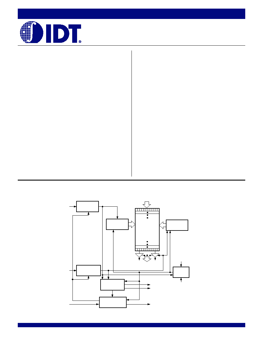
DESCRIPTION:
The IDT7200/7201/7202 are dual-port memories that load and empty data
on a first-in/first-out basis. The devices use Full and Empty flags to prevent data
overflow and underflow and expansion logic to allow for unlimited expansion
capability in both word size and depth.
The reads and writes are internally sequential through the use of ring
pointers, with no address information required to load and unload data. Data
is toggled in and out of the devices through the use of the Write (
W) and Read
(
R) pins.
The devices utilize a 9-bit wide data array to allow for control and parity bits
at the user's option. This feature is especially useful in data communications
applications where it is necessary to use a parity bit for transmission/reception
error checking. It also features a Retransmit (
RT) capability that allows for reset
of the read pointer to its initial position when
RT is pulsed LOW to allow for
retransmission from the beginning of data. A Half-Full Flag is available in the
single device mode and width expansion modes.
These FIFOs are fabricated using IDT's high-speed CMOS technology.
They are designed for those applications requiring asynchronous and
simultaneous read/writes in multiprocessing and rate buffer applications.
Military grade product is manufactured in compliance with the latest revision of
MIL-STD-883, Class B.
FUNCTIONAL BLOCK DIAGRAM
W
WRITE
CONTROL
READ
CONTROL
R
FLAG
LOGIC
EXPANSION
LOGIC
XI
WRITE
POINTER
RAM
ARRAY
256 x 9
512 x 9
1,024 x 9
READ
POINTER
DATA INPUTS
RESET
LOGIC
THREE-
STATE
BUFFERS
DATA OUTPUTS
EF
FF
XO/HF
RS
FL/RT
(D
0
-D
8
)
2679 drw 01
(Q
0
-Q
8
)
2
COMMERCIAL, INDUSTRIAL AND MILITARY
TEMPERATURE RANGES
IDT7201L/7201LA/7202LA CMOS ASYNCHRONOUS FIFO
256 x 9, 512 x 9 and 1,024 x 9
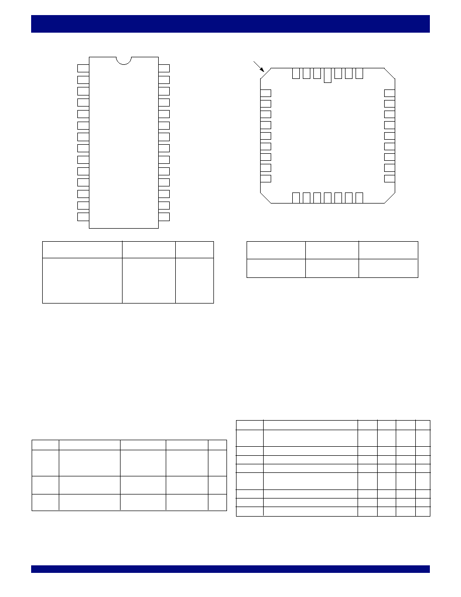
PIN CONFIGURATIONS
RECOMMENDED DC OPERATING
CONDITIONS
Symbol
Parameter
Min.
Typ.
Max. Unit
V
CC
Supply Voltage
4.5
5.0
5.5
V
Commercial/Industrial/Military
GND
Supply Voltage
0
0
0
V
V
IH
(1)
Input High Voltage Com'l/Ind'l
2.0
--
--
V
V
IH
(1)
Input High Voltage Military
2.2
--
--
V
V
IL
(2)
Input Low Voltage
--
--
0.8
V
Commercial/Industrial/Military
T
A
Operating Temperature Commercial
0
--
70
įC
T
A
Operating Temperature Industrial
≠40
--
85
įC
T
A
Operating Temperature Military
≠55
--
125
įC
NOTES:
1. For
RT/RS/XI input, V
IH
= 2.6V (commercial).
For
RT/RS/XI input, V
IH
= 2.8V (military).
2. 1.5V undershoots are allowed for 10ns once per cycle.
ABSOLUTE MAXIMUM RATINGS
Symbol
Rating
Com'l & Ind'l
Mil.
Unit
V
TERM
Terminal Voltage
≠0.5 to +7.0
≠0.5 to +7.0
V
with Respect
to GND
T
STG
Storage
≠55 to +125
≠65 to +155
įC
Temperature
I
OUT
DC Output
≠50 to +50
≠50 to +50
mA
Current
NOTE:
1. Stresses greater than those listed under ABSOLUTE MAXIMUM RATINGS may cause
permanent damage to the device. This is a stress rating only and functional operation of
the device at these or any other conditions above those indicated in the operational
sections of this specification is not implied. Exposure to absolute maximum rating
conditions for extended periods may affect reliability.
Reference
Order
Package Type
Identifier
Code
PLASTIC DIP
(1)
P28-1
P
PLASTIC THIN DIP
P28-2
T P
CERDIP
(1)
D28-1
D
THIN CERDIP
D28-3
TD
SOIC
SO28-3
SO
TOP VIEW
Reference
Order
Package Type
Identifier
Code
LCC
(1)
L32- 1
L
PLCC
J32-1
J
TOP VIEW
NOTE:
1. The 600-mil-wide DIP (P28-1 and D28-1) and LCC are not available for the IDT7200.
W
D
8
V
CC
D
4
1
2
28
27
D
3
D
5
3
26
D
2
D
6
4
25
D
1
D
7
5
24
D
0
FL/RT
6
23
XI
RS
7
22
FF
EF
8
21
Q
0
XO/HF
9
20
Q
1
Q
7
10
19
Q
2
Q
6
11
18
Q
3
Q
5
12
17
Q
8
Q
4
13
16
GND
R
14
15
2679 drw 02a
D
2
5
D
1
6
D
0
7
XI
8
FF
9
Q
0
10
Q
1
11
NC
12
Q
2
13
D
6
D
7
NC
FL/RT
RS
EF
XO/HF
Q
7
Q
6
29
28
27
26
25
24
23
22
21
4
3
2
1
32 31 30
14 15 16 17 18 19 20
Q
3
Q
8
GND
NC
R
Q
4
Q
5
D
3
D
8
W
NC
V
CC
D
4
D
5
INDEX
2679 drw 02b

3
COMMERCIAL, INDUSTRIAL AND MILITARY
TEMPERATURE RANGES
IDT7201L/7201LA/7202LA CMOS ASYNCHRONOUS FIFO
256 x 9, 512 x 9 and 1,024 x 9
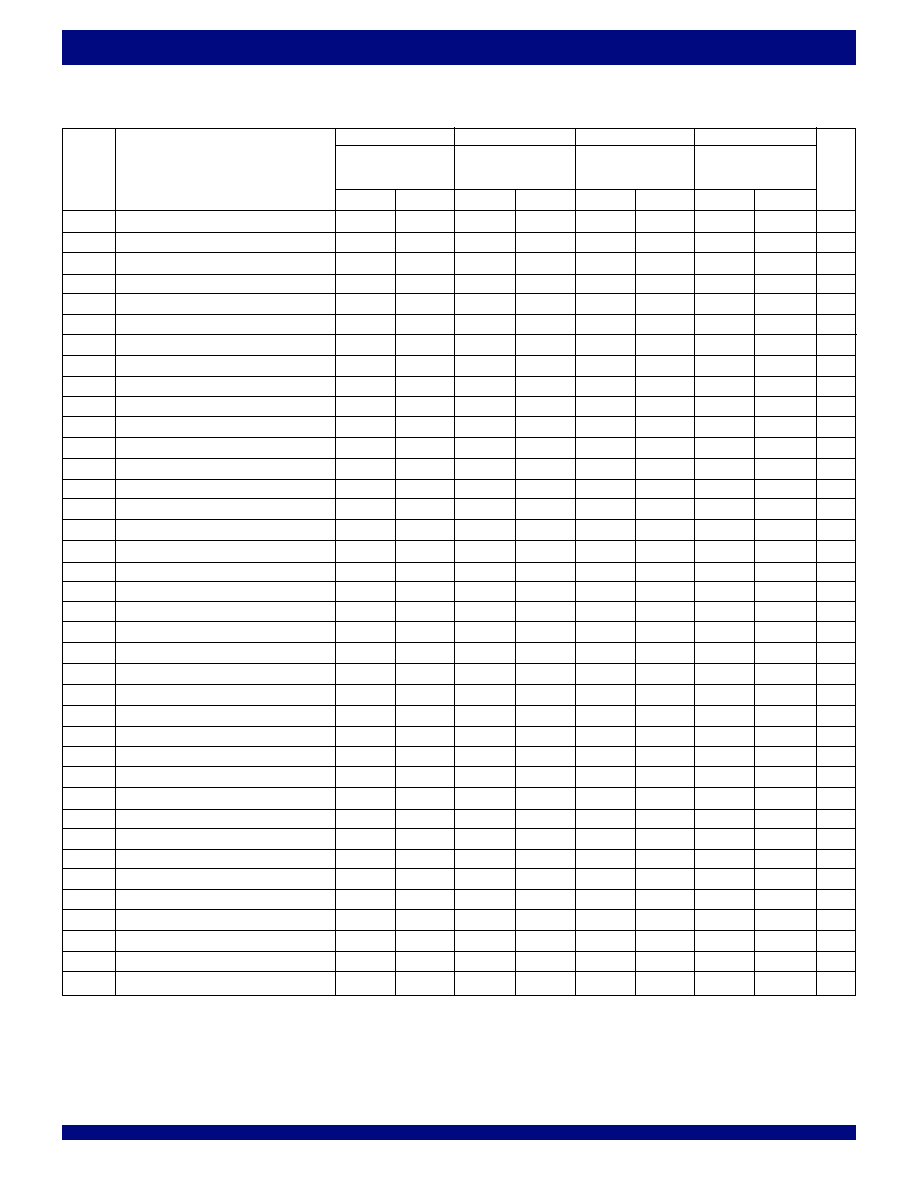
DC ELECTRICAL CHARACTERISTICS
(Commercial: V
CC
= 5V Ī 10%, T
A
= 0
o
C to +70
o
C; Industrial: V
CC
= 5V Ī 10%, T
A
= ≠40
o
C to +85
o
C; Military: V
CC
= 5V Ī 10%, T
A
= ≠55
o
C to +125
o
C)
IDT7200L
IDT7200L
IDT7201LA
IDT7201LA
IDT7202LA
IDT7202LA
Com'l & Ind'l
(1)
Military
(2)
t
A
= 12, 15, 20, 25, 35, 50 ns
t
A
= 20, 30, 50, 80 ns
Symbol
Parameter
Min.
Max.
Min.
Max.
Unit
I
LI
(3)
Input Leakage Current (Any Input)
≠1
1
≠10
10
Ķ A
I
LO
(4)
Output Leakage Current
≠10
10
≠10
10
Ķ A
V
OH
Output Logic "1" Voltage I
OH
= ≠2mA
2.4
--
2.4
--
V
V
OL
Output Logic "0" Voltage I
OL
= 8mA
--
0.4
--
0.4
V
I
CC1
(5,6,7)
Active Power Supply Current
--
80
--
100
mA
I
CC2
(5,8)
Standby Current (
R=W=RS=FL/RT=V
IH
)
--
5
--
15
mA
NOTES:
1. Industrial temperature range product for the 15ns and 25 ns speed grades are available as a standard device.
2. Military speed grades of 50ns and 80ns are only available for the IDT7201LA.
3. Measurements with 0.4
V
IN
V
CC
.
4.
R
V
IH
, 0.4
V
OUT
V
CC
.
5. Tested with outputs open (I
OUT
= 0).
6. Tested at f = 20 MHz.
7. Typical I
CC1
= 15 + 2*f
S
+ 0.02*C
L
*f
S
(in mA) with V
CC
= 5V, T
A
= 25
į
C, f
S
= WCLK frequency = RCLK frequency (in MHz, using TTL levels), data switching at f
S
/2, C
L
= capacitive
load (in pF).
8. All Inputs = V
CC
- 0.2V or GND + 0.2V.
AC TEST CONDITIONS
Input Pulse Levels
GND to 3.0V
Input Rise/Fall Times
5ns
Input Timing Reference Levels
1.5V
Output Reference Levels
1.5V
Output Load
See Figure 1
Symbol
Parameter
Condition
Max.
Unit
C
IN
Input Capacitance
V
IN
= 0V
8
pF
C
OUT
Output Capacitance
V
OUT
= 0V
8
pF
NOTE:
1. Characterized values, not currently tested.
CAPACITANCE
(T
A
= +25
įC, f = 1.0 MHz)
or equivalent circuit
2679 drw 03
30pF*
1.1K
5V
TO
OUTPUT
PIN
680
Figure 1. Output Load
* Includes scope and jig capacitances.
4
COMMERCIAL, INDUSTRIAL AND MILITARY
TEMPERATURE RANGES
IDT7201L/7201LA/7202LA CMOS ASYNCHRONOUS FIFO
256 x 9, 512 x 9 and 1,024 x 9
Commercial
Com'l & Ind'l
(2)
Com'l & Mil.
Com'l & Ind'l
(2)
IDT7200L12
IDT7200L15
IDT7200L20
IDT7200L25
IDT7201LA12
IDT7201LA15
IDT7201LA20
IDT7201LA25
IDT7202LA12
IDT7202LA15
IDT7202LA20
IDT7202LA25
Symbol
Parameter
Min.
Max.
Min.
Max.
Min.
Max.
Min.
Max.
Unit
t
S
Shift Frequency
--
50
--
40
--
33.3
--
28.5
MHz
t
RC
Read Cycle Time
20
--
25
--
30
--
35
--
ns
t
A
Access Time
--
12
--
15
--
20
--
25
ns
t
RR
Read Recovery Time
8
--
10
--
10
--
10
--
ns
t
RPW
Read Pulse Width
(3)
12
--
15
--
20
--
25
--
ns
t
RLZ
Read Pulse Low to Data Bus at Low Z
(4)
3
--
3
--
3
--
3
--
ns
t
WLZ
Write Pulse High to Data Bus at Low Z
(4,5)
5
--
5
--
5
--
5
--
ns
t
DV
Data Valid from Read Pulse High
5
--
5
--
5
--
5
--
ns
t
RHZ
Read Pulse High to Data Bus at High Z
(4)
--
12
--
15
--
15
--
18
ns
t
WC
Write Cycle Time
20
--
25
--
30
--
35
--
ns
t
WPW
Write Pulse Width
(3)
12
--
15
--
20
--
25
--
ns
t
WR
Write Recovery Time
8
--
10
--
10
--
10
--
ns
t
DS
Data Set-up Time
9
--
11
--
12
--
15
--
ns
t
DH
Data Hold Time
0
--
0
--
0
--
0
--
ns
t
RSC
Reset Cycle Time
20
--
25
--
30
--
35
--
ns
t
RS
Reset Pulse Width
(3)
12
--
15
--
20
--
25
--
ns
t
RSS
Reset Set-up Time
(4)
12
--
15
--
20
--
25
--
ns
t
RSR
Reset Recovery Time
8
--
10
--
10
--
10
--
ns
t
RTC
Retransmit Cycle Time
20
--
25
--
30
--
35
--
ns
t
RT
Retransmit Pulse Width
(3)
12
--
15
--
20
--
25
--
ns
t
RTS
Retransmit Set-up Time
(4)
12
--
15
--
20
--
25
--
ns
t
RTR
Retransmit Recovery Time
8
--
10
--
10
--
10
--
ns
t
EFL
Reset to Empty Flag Low
--
12
--
25
--
30
--
35
ns
t
HFH,FFH
Reset to Half-Full and Full Flag High
--
17
--
25
--
30
--
35
ns
t
RTF
Retransmit Low to Flags Valid
--
20
--
25
--
30
--
35
ns
t
REF
Read Low to Empty Flag Low
--
12
--
15
--
20
--
25
ns
t
RFF
Read High to Full Flag High
--
14
--
15
--
20
--
25
ns
t
RPE
Read Pulse Width after
EF High
12
--
15
--
20
--
25
--
ns
t
WEF
Write High to Empty Flag High
--
12
--
15
--
20
--
25
ns
t
WFF
Write Low to Full Flag Low
--
14
--
15
--
20
--
25
ns
t
WHF
Write Low to Half-Full Flag Low
--
17
--
25
--
30
--
35
ns
t
RHF
Read High to Half-Full Flag High
--
17
--
25
--
30
--
35
ns
t
WPF
Write Pulse Width after
FF High
12
--
15
--
20
--
25
--
ns
t
XOL
Read/Write to
XO Low
--
12
--
15
--
20
--
25
ns
t
XOH
Read/Write to
XO High
--
12
--
15
--
20
--
25
ns
t
XI
XI Pulse Width
(3)
12
--
15
--
20
--
25
--
ns
t
XIR
XI Recovery Time
8
--
10
--
10
--
10
--
ns
t
XIS
XI Set-up Time
8
--
10
--
10
--
10
--
ns
NOTES:
1. Timings referenced as in AC Test Conditions.
2. Industrial temperature range product for 15ns and 25ns speed grades are available as a standard device.
3. Pulse widths less than minimum value are not allowed.
4. Values guaranteed by design, not currently tested.
5. Only applies to read data flow-through mode
AC ELECTRICAL CHARACTERISTICS
(1)
(Commercial: V
CC
= 5V Ī 10%, T
A
= 0
įC to +70įC; Industrial: V
CC
= 5V Ī 10%, T
A
= ≠40
įC to +85įC; Military: V
CC
= 5V Ī 10%, T
A
= ≠55
įC to +125įC)
5
COMMERCIAL, INDUSTRIAL AND MILITARY
TEMPERATURE RANGES
IDT7201L/7201LA/7202LA CMOS ASYNCHRONOUS FIFO
256 x 9, 512 x 9 and 1,024 x 9
Military
Commercial
Com'l & Mil.
(2)
Military
(2)
IDT7200L30
IDT7200L35
IDT7200L50
IDT7201LA30
IDT7201LA35
IDT7201LA50
IDT7202LA30
IDT7202LA35
IDT7202LA50
IDT7201LA80
Symbol
Parameter
Min.
Max.
Min.
Max.
Min.
Max.
Min.
Max.
Unit
t
S
Shift Frequency
--
25
--
22.2
--
15
--
10
MHz
t
RC
Read Cycle Time
40
--
45
--
65
--
100
--
ns
t
A
Access Time
--
30
--
35
--
50
--
80
ns
t
RR
Read Recovery Time
10
--
10
--
15
--
20
--
ns
t
RPW
Read Pulse Width
(3)
30
--
35
--
50
--
80
--
ns
t
RLZ
Read Pulse Low to Data Bus at Low Z
(4)
3
--
3
--
3
--
3
--
ns
t
WLZ
Write Pulse High to Data Bus at Low Z
(4, 5)
5
--
5
--
5
--
5
--
ns
t
DV
Data Valid from Read Pulse High
5
--
5
--
5
--
5
--
ns
t
RHZ
Read Pulse High to Data Bus at High Z
(4)
--
20
--
20
--
30
--
30
ns
t
WC
Write Cycle Time
40
--
45
--
65
--
100
--
ns
t
WPW
Write Pulse Width
(3)
30
--
35
--
50
--
80
--
ns
t
WR
Write Recovery Time
10
--
10
--
15
--
20
--
ns
t
DS
Data Set-up Time
18
--
18
--
30
--
40
--
ns
t
DH
Data Hold Time
0
--
0
--
5
--
10
--
ns
t
RSC
Reset Cycle Time
40
--
45
--
65
--
100
--
ns
t
RS
Reset Pulse Width
(3)
30
--
35
--
50
--
80
--
ns
t
RSS
Reset Set-up Time
(4)
30
--
35
--
50
--
80
--
ns
t
RSR
Reset Recovery Time
10
--
10
--
15
--
20
--
ns
t
RTC
Retransmit Cycle Time
40
--
45
--
65
--
100
--
ns
t
RT
Retransmit Pulse Width
(3)
30
--
35
--
50
--
80
--
ns
t
RTS
Retransmit Set-up Time
(4)
30
--
35
--
50
--
80
--
ns
t
RTR
Retransmit Recovery Time
10
--
10
--
15
--
20
--
ns
t
EFL
Reset to Empty Flag Low
--
40
--
45
--
65
--
100
ns
t
HFH,FFH
Reset to Half-Full and Full Flag High
--
40
--
45
--
65
--
100
ns
t
RTF
Retransmit Low to Flags Valid
--
40
--
45
--
65
--
100
ns
t
REF
Read Low to Empty Flag Low
--
30
--
30
--
45
--
60
ns
t
RFF
Read High to Full Flag High
--
30
--
30
--
45
--
60
ns
t
RPE
Read Pulse Width after
EF High
30
--
35
--
50
--
80
--
ns
t
WEF
Write High to Empty Flag High
--
30
--
30
--
45
--
60
ns
t
WFF
Write Low to Full Flag Low
--
30
--
30
--
45
--
60
ns
t
WHF
Write Low to Half-Full Flag Low
--
40
--
45
--
65
--
100
ns
t
RHF
Read High to Half-Full Flag High
--
40
--
45
--
65
--
100
ns
t
WPF
Write Pulse Width after
FF High
30
--
35
--
50
--
80
--
ns
t
XOL
Read/Write to
XO Low
--
30
--
35
--
50
--
80
ns
t
XOH
Read/Write to
XO High
--
30
--
35
--
50
--
80
ns
t
XI
XI Pulse Width
(3)
30
--
35
--
50
--
80
--
ns
t
XIR
XI Recovery Time
10
--
10
--
10
--
10
--
ns
t
XIS
XI Set-up Time
10
--
10
--
15
--
15
--
ns
AC ELECTRICAL CHARACTERISTICS
(1)
(Continued)
(Commercial: V
CC
= 5V Ī 10%, T
A
= 0
įC to +70įC; Industrial: V
CC
= 5V Ī 10%, T
A
= ≠40
įC to +85įC; Military: V
CC
= 5V Ī 10%, T
A
= ≠55
įC to +125įC)
NOTES:
1. Timings referenced as in AC Test Conditions
2. Military speed grades of 50ns and 80ns are only available for IDT7201LA.
3. Pulse widths less than minimum value are not allowed.
4. Values guaranteed by design, not currently tested.
5. Only applies to read data flow-through mode.