 | –≠–ª–µ–∫—Ç—Ä–æ–Ω–Ω—ã–π –∫–æ–º–ø–æ–Ω–µ–Ω—Ç: 72103 | –°–∫–∞—á–∞—Ç—å:  PDF PDF  ZIP ZIP |

Integrated Device Technology, Inc.
IDT72103
IDT72104
CMOS PARALLEL-SERIAL FIFO
2,048 x 9 and 4,096 x 9
FEATURES:
∑
35ns parallel port access time, 45ns cycle time
∑
50MHz serial input/output frequency
∑
Serial-to-parallel, parallel-to-serial, serial-to-serial, and
parallel-to-parallel operations
∑
Expandable in both depth and width with no external
components
∑
FlexishiftTM -- Sets programmable serial word width
from 4 bits to any width with no external components
∑
Multiple flags: Full, Almost-Full (Full-1/8),Full-Minus-
One, Empty, Almost-Empty (Empty + 1/8), Empty-Plus-
One, and Half-Full
∑
Asynchronous and simultaneous read or write operations
∑
Dual-Port, zero fall-through time architecture
∑
Retransmit capability in single-device mode
∑
Packaged in 44-pin PLCC
∑
Industrial temperature range (≠40
o
C to +85
o
C)
APPLICATIONS:
∑
High-speed data acquisition systems
∑
Local area network (LAN) buffer
∑
High-speed modem data buffer
∑
Remote telemetry data buffer
∑
FAX raster video data buffer
∑
Laser printer engine data buffer
∑
High-speed parallel bus-to-bus communications
∑
Magnetic media controllers
∑
Serial link buffer
DESCRIPTION:
The IDT72103/72104 are high-speed Parallel-Serial FlFOs
to be used with high-performance systems for functions such
as serial communications, laser printer engine control and
local area networks.
The IDT logo is a registered trademark of Integrated Device Technology,Inc.
For latest information contact IDT's web site at www.idt.com or fax-on-demand at 408-492-8391.
FUNCTIONAL BLOCK DIAGRAM
2753 drw 01
DATA INPUTS (D
0
-D
RAM ARRAY
2048 x 9
4096 x 9
WRITE
POINTER
READ
POINTER
FLAG
LOGIC
8
DEPTH
EXPANSION
LOGIC
/
SERIAL
OUTPUT
CIRCUITRY
SOX
SO
RESET
LOGIC
SOCP
SERIAL
OUTPUT
DATA OUTPUTS (Q
0
-Q
8
SERIAL/
PARALLEL
CONTROL
/PO
/PI
SERIAL
INPUT
CIRCUITRY
SIX
SI
SICP
SERIAL
INPUT
)
)
INDUSTRIAL TEMPERATURE RANGE
DECEMBER 1999
©1999 Integrated Device Technology, Inc.
DSC-2753/-
1

2
IDT72103, IDT72104
CMOS PARALLEL-SERIAL FIFO 2,048 x 9, 4,096 x 9
INDUSTRIAL TEMPERATURE RANGE
DESCRIPTION (Continued)
A serial input, a serial output and two 9-bit parallel ports
make four modes of data transfer possible: serial-to-parallel,
parallel-to-serial, serial-to-serial, and parallel-to-parallel. These
devices are expandable in both depth and width for all of these
operational configurations.
These FIFOs may be configured to handle serial word
widths of four or greater using IDT's unique Flexishift feature.
Flexishift allows serial width and depth expansion without
external components. For example, you may configure a 4K
x 24 FIFO using three IDT72104s in a serial width expansion
configuration.
PLCC (J44-1, order code: J)
TOP VIEW
7
8
9
10
11
12
13
39
38
37
36
35
34
33
4
3
2
1
43
INDEX
5
6
44
42 41 40
14
15
16
17
32
31
30
29
18 19 20 21 22 23 24 25 26 27 28
D
0
/PO
SOX
SOCP
Q
0
SO
GND
/
SI
SICP
SIX
GND
/
Q
1
Q
2
Q
3
Q
4
GND
Q
5
Q
6
Q
7
Q
8
GND
V
D
1
D
2
D
3
D
4
CC
D
5
D
6
D
7
D
8
GND
2753 drw 03
PIN CONFIGURATIONS
Seven flags are provided to signal memory status of the
FIFO. The flags are
FF
(Full),
AF
(7/8 full),
FF≠1
(Full-minus-
one),
EF
(Empty),
AE
(1/8 full),
EF+1
(Empty-plus-one), and
HF
(Half-full).
Read (
R
) and Write (
W
) control pins are provided for
asynchronous and simultaneous operations. An Output En-
able (
OE
) control pin is available on the parallel output port for
high-impedance control. The depth expansion control pins
XO
and
Xl
are provided to allow cascading for deeper FlFOs.
The IDT72103/72104 are manufactured using IDT's CMOS
technology.

IDT72103, IDT72104
CMOS PARALLEL-SERIAL FIFO 2,048 x 9 AND 4,096 x 9
INDUSTRIAL TEMPERATURE RANGE
3
PIN DESCRIPTION
Symbol
Name
I/O
Description
D
0
-D
8
Data Inputs
I/O In a parallel input configuration ≠ data inputs for 9-bit wide data.
Serial Input Word
In a serial input configuration ≠ one of the nine output pins is used to select the serial input
Width Select
word width.
RS
Reset
I
When
RS
is set low, internal READ and WRITE pointers are set to the first location of the RAM
array.
EF
,
EF+1
,
AEF
are all LOW after a reset, while
FF
,
FF-1
,
HF
are HIGH after a reset.
W
Write
I
A parallel word write cycle is initiated on the falling edge of
W
if the
FF
is high. When the FIFO
is full,
FF
will go low inhibiting further write operations to prevent data overflow. In a serial
input configuration, data bits are clocked into the input shift register and the write pointer does
not advance until a full parallel word is assembled. One of the pins, D
i
, is connected to
W
and
advances the write pointer every i-th serial input clock.
R
Read
I
A read cycle is initiated on the falling edge of
R
if the
EF
is HIGH. After all the data from the
FIFO has been read
EF
will go LOW inhibiting further read operations. In a serial output
configuration, a data word is read from memory into the output shift register. One of the pins,
Q
j
, is connected to
R
and advances the read pointer every j-th serial output clock.
FL
/
RT
First Load/
I
This is a dual-purpose pin. In multiple-device mode,
FL
/
RT
is grounded to indicate the first
Retransmit
device loaded. In single-device mode,
FL
/
RT
acts as the retransmit input. Single-device mode
is initiated by grounding the
XI
pin.
Xl
Expansion In
I
In single-device mode,
XI
is grounded. In depth expansion or daisy chain mode,
XI
is con-
nected to the
XO
pin of the previous device.
OE
Output Enable
I
When
OE
is LOW, both parallel and serial outputs are enabled. When
OE
is HIGH, the parallel
output buffers are placed in a high-impedance state.
Q
0
-Q
8
Data Outputs/Serial
O
In a parallel output configuration - data outputs for 9-bit wide data. In a serial output
Output Word Width Select
configuration - one of nine output pins used to select the serial output word width.
FF
Full Flag
O
FF
is asserted LOW when the FIFO is full and further write operations are inhibited. When
the
FF
is HIGH, the FIFO is not full and data can be written into the FIFO.
FF-1
Full-1 Flag
O
FF-1
goes LOW when the FIFO memory array is one word away from being full. It will remain
LOW when every memory location is filled.
XO
/
HF
Expansion Out/
O
HF
is LOW when the FIFO is more than half-full in the single device or width expansion modes.
Half-Full Flag
The
HF
will remain LOW until the difference between the write and read pointers is less than
or equal to one-half of the FIFO memory.
In depth expansion mode, a pulse is written from
XO
to
XI
of the next device when the last
location in the FIFO is filled. Another pulse is sent from
XO
to
Xl
of the next device when the
last FIFO location is read.
AEF
Almost-Empty/
O
When
AEF
is LOW, the FIFO is empty to 1/8 full or 7/8 full to completely full. If
AEF
is HIGH,
Almost-Full Flag
then the FIFO is greater than 1/8 full, but less than 7/8 full.
EF+1
Empty+1 Flag
O
EF+ 1
is LOW when there is zero or one word in the FIFO memory array.
EF
Empty Flag
O
EF
goes LOW when the FIFO is empty and further read operations are inhibited.
FF
is HIGH
when the FIFO is not empty and data reads are permitted.
Sl
Serial Input Expansion
I
Data input for serial data.
SO
Serial Output Expansion
O
Data output for serial data.
SICP
Serial Input Clock
I
This pin is the serial input clock. On the rising edge of the SICP signal, new serial data bits
are read into the serial input shift register.
SOCP Serial Output
I
This pin is the serial output clock. On the rising edge of the SOCP signal, new serial data bits
Clock
are read from the serial output shift register.
SIX
Serial Input
I
SIX controls the serial input expansion for word widths greater than 9 bits. In a serial input
Expansion
configuration, the SIX pin of the least significant device is tied HIGH. The SIX pin of all other
devices is connected to the D
8
pin of the previous device. In parallel input configurations or
serial input configurations of 9 bits or less, SIX is tied HIGH.
SOX
Serial Output
I
SOX controls the serial output expansion for word widths greater than 9 bits. In a serial output
Expansion
configuration, the SOX pin of the least significant device is tied HIGH. The SOX pin of all other
devices is connected to the Q
8
pin of the previous device. In parallel output configurations or
serial output configurations of 9 bits or less, SOX is tied HIGH.
SI
/PI
Serial/Parallel Input
I
When this pin is HIGH, the FIFO is in a parallel input configuration and accepts input data through
D
0
-D
8
. When
SI
/PI is LOW, the FIFO is in a serial input configuration and data is input through Sl.
SO
/PO Serial/Parallel Output
I
When this pin is HIGH, the FIFO is in a parallel output configuration and sends output data through
Q
0
-Q
8
. When
SO
/PO is LOW the FIFO is in a serial output configuration and data is input through SO.
GND
Ground
Five ground pins for the PLCC.
V
CC
Power
One + 5V power pin.
2753 tbl 04
4
IDT72103, IDT72104
CMOS PARALLEL-SERIAL FIFO 2,048 x 9, 4,096 x 9
INDUSTRIAL TEMPERATURE RANGE
ABSOLUTE MAXIMUM RATINGS
(1)
Symbol
Rating
Commercial
Unit
V
TERM
Terminal Voltage
≠0.5 to +7.0
V
with Respect to GND
T
STG
Storage Temperature
≠55 to +125
∞
C
I
OUT
DC Output Current
≠50 to +50
mA
NOTE:
2753 tbl 01
1.Stresses greater than those listed under ABSOLUTE MAXIMUM
RATINGS may cause permanent damage to the device. This is a stress
rating only and functional operation of the device at these or any other
conditions above those indicated in the operational sections of this
specification is not implied. Exposure to absolute maximum rating
conditions for extended periods may affect reliability.
RECOMMENDED DC OPERATING CONDITIONS
Symbol
Parameter
Min.
Typ.
Max. Unit
V
CC
Commercial Supply
4.5
5.0
5.5
V
Voltage
GND
Supply Voltage
0
0
0
V
V
IH
Input High Voltage
2.0
--
--
V
Commercial
V
IL
(1)
Input Low Voltage
--
--
0.8
V
T
A
Operating Temperature
-40
--
85
∞
C
Industrial
NOTE:
2753 tbl 03
1. 1.5V undershoots are allowed for 10ns once per cycle.
CAPACITANCE
(T
A
= +25
∞
C, f = 1.0MHz)
Symbol
Parameter
(1)
Conditions
Max.
Unit
C
IN
Input Capacitance
V
IN
= 0V
10
pF
C
OUT
Output Capacitance
V
OUT
= 0V
12
pF
NOTE:
2753 tbl 02
1. This parameter is sampled and not 100% tested.
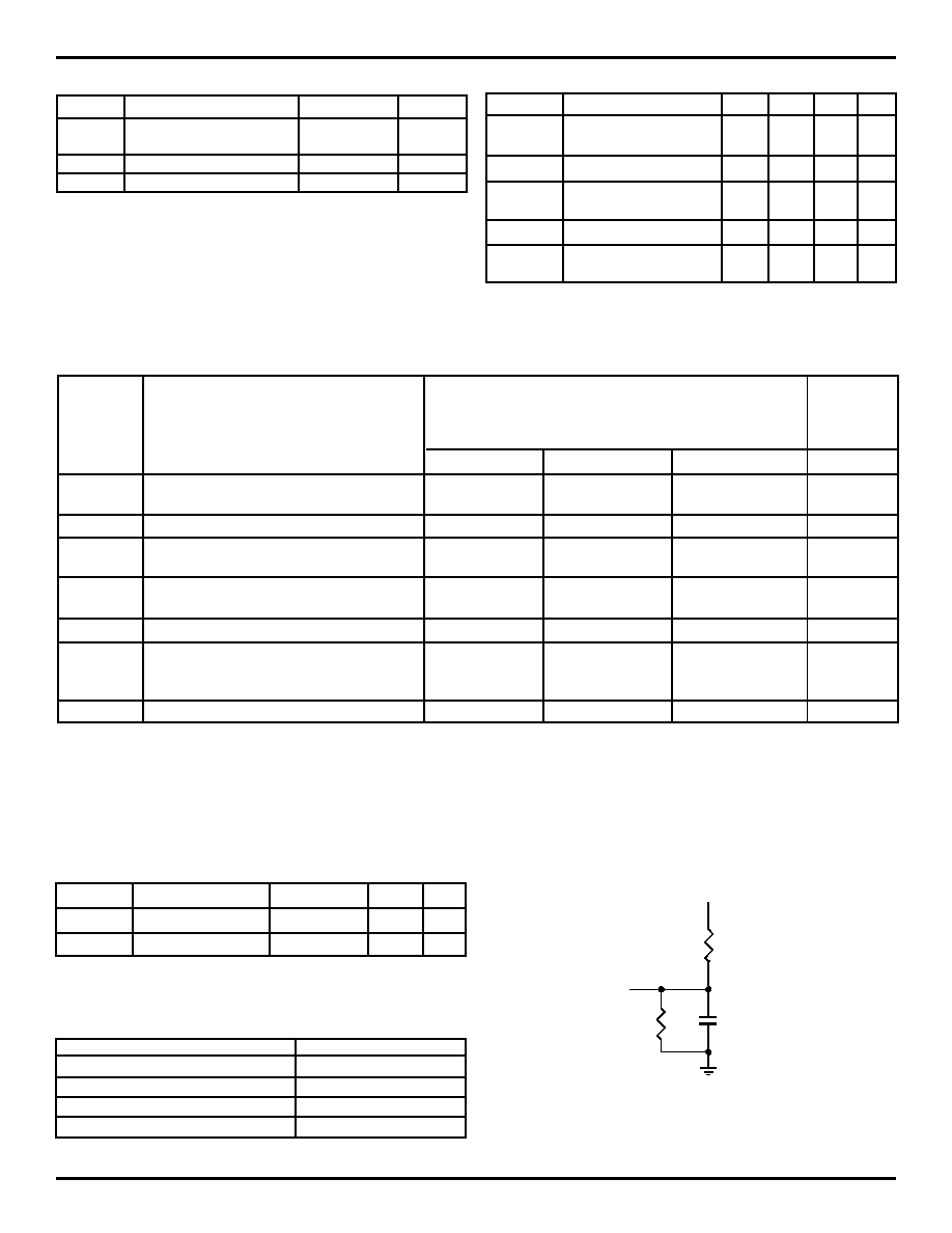
AC TEST CONDITIONS
Input Pulse Levels
GND to 3.0V
Input Rise/Fall Times
3ns
Input Timing Reference Levels
1.5V
Output Reference Levels
1.5V
Output Load
See Figure 1
2753 tbl 07
Figure 1. Ouput Load
*Including jig and scope capacitances
or equivalent circuit
1.1K
30pF*
680
5V
D.U.T.
2753 drw 04
IDT72103
IDT72104
Industrial
t
A
= 35, 50ns
Symbol
Parameter
Min.
Typ.
Max.
Unit
I
LI
(1)
Input Leakage Current (Any Input)
≠1
--
1
µ
A
I
LO
(2)
Output Leakage Current
≠10
--
10
µ
A
V
OH
Output Logic "1" Voltage,
2.4
--
--
V
I
OUT
= ≠2mA
(4)
V
OL
Output Logic "0" Voltage,
--
--
0.4
V
I
OUT
= 8mA
(5)
I
CC1
(3)
Active Power Supply Current
--
90
140
mA
I
CC2
(3,6)
Standby Current
--
8
12
mA
(
R
=
W
=
RS
=
FL
/
RT
= V
IH
)
(SOCP = SICP = V
IL
)
I
CC3
(3,6)
Power Down Current
--
--
2
mA
NOTES:
2753 tbl 06
1. Measurements with 0.4
V
IN
V
CC
.
2.
R
V
IH
, SOCP
V
IL
, 0.4
V
OUT
V
CC
.
3. Tested with outputs open (I
OUT
= 0).
4. For SO, I
OUT
= ≠8mA.
5. For SO, I
OUT
=16mA.
6. SOCP = SICP
0.2V; other Inputs = V
CC
- 0.2V.
DC ELECTRICAL CHARACTERISTICS
(Industrial: V
CC
= 5.0V
±
10%, T
A
= -40
∞
C to +85
∞
C)

IDT72103, IDT72104
CMOS PARALLEL-SERIAL FIFO 2,048 x 9 AND 4,096 x 9
INDUSTRIAL TEMPERATURE RANGE
5
AC ELECTRICAL CHARACTERISTICS
(Industrial: V
CC
= 5.0V
±
10%, T
A
= -40
∞
C to +85
∞
C)
Industrial
IDT72103L35
IDT72103L50
IDT72104L35
IDT72104L50
Timing
Symbol
Parameter
Min.
Max.
Min.
Max.
Unit
Figure
f
S
Parallel Shift Frequency
--
22.2
--
15
MHz
--
f
SOCP
Serial-Out Shift Frequency
--
50
--
40
MHz
--
f
SICP
Serial-In Shift Frequency
--
50
--
40
MHz
--
PARALLEL-OUTPUT MODE TIMINGS
t
A
Access Time
--
35
--
50
ns
4
t
RR
Read Recovery Time
10
--
15
--
ns
4
t
RPW
Read Pulse Width
35
--
50
--
ns
4
t
RC
Read Cycle Time
45
--
65
--
ns
4
t
WLZ
Write Pulse LOW to Data Bus at Low-Z
(1)
5
--
15
--
ns
15
t
RLZ
Read Pulse LOW to Data Bus at Low-Z
(1)
5
--
10
--
ns
4
t
RHZ
Read Pulse HIGH to Data Bus at High-Z
(1)
--
20
--
30
ns
4
t
DV
Data Valid from Read Pulse HIGH
5
--
5
--
ns
4
PARALLEL-INPUT MODE TIMINGS
t
DS
Data Set-up Time
18
--
20
--
ns
3
t
DH
Data Hold Time
0
--
0
--
ns
3
t
WC
Write Cycle Time
45
--
50
--
ns
3
t
WPW
Write Pulse Width
35
--
40
--
ns
3
t
WR
Write Recovery Time
10
--
10
--
ns
3
RESET TIMINGS
t
RSC
Reset Cycle Time
45
--
50
--
ns
2,18
t
RS
Reset Pulse Width
35
--
40
--
ns
2,18
t
RSS
Reset Set-up Time
35
--
40
--
ns
2,18
t
RSR
Reset Recovery Time
10
--
10
--
ns
2,17,18
RESET TO FLAG TIMINGS
t
RSF1
Reset to
EF
,
AEF
, and
EF+1
LOW
--
45
--
65
ns
2
t
RSF2
Reset to
HF
,
FF
, and
FF-1
LOW
--
45
--
65
ns
2
RESET TO OUTPUT TIMINGS ≠ SERIAL MODE ONLY
t
RSQL
Reset Going LOW to Q
0-8
LOW
20
--
20
--
ns
18
t
RSQH
Reset Going HIGH to Q
0-8
HIGH
20
--
20
--
ns
18
t
RSDL
Reset Going LOW to D
0-8
LOW
20
--
20
--
ns
17
RETRANSMIT TIMINGS
t
RTC
Retransmit Cycle Time
45
--
50
--
ns
5
t
RT
Retransmit Pulse Width
35
--
40
--
ns
5
t
RTS
Retransmit Set-up Time
35
--
40
--
ns
5
t
RTR
Retransmit Recovery Time
10
--
10
--
ns
5
t
RTF
Retransmit to Flags
--
35
--
50
ns
5
PARALLEL MODE FLAG TIMINGS
t
REF
Read LOW to
EF
LOW
--
30
--
45
ns
6
t
RFF
Read HIGH to
FF
HIGH
--
30
--
45
ns
7
t
RF
Read HIGH to Transitioning
HF
,
AEF
and
FF-1
--
45
--
65
ns
8,9,10
t
RE
Read LOW to
EF+1
LOW
--
45
--
65
ns
11
t
RPE
Read Pulse Width after
EF
HIGH
35
--
40
--
ns
15
t
WEF
Write HIGH to
EF
HIGH
--
30
--
45
ns
6
t
WFF
Write LOW to
FF
LOW
--
30
--
45
ns
7
t
WF
Write LOW to Transitioning
HF
,
AEF
and
FF-1
--
45
--
65
ns
8,9,10
t
WE
Write HIGH to
EF+1
HIGH
--
45
--
65
ns
11
t
WPF
Write Pulse Width after
FF
HIGH
35
--
40
--
ns
16
2753 tbl 08
NOTE:
1. Values guaranteed by design, not tested.