 | –≠–ª–µ–∫—Ç—Ä–æ–Ω–Ω—ã–π –∫–æ–º–ø–æ–Ω–µ–Ω—Ç: 7217 | –°–∫–∞—á–∞—Ç—å:  PDF PDF  ZIP ZIP |

1
COMMERCIAL TEMPERATURE RANGE
IDT7217L
16 x 16 PARALLEL CMOS MULTIPLIERS
DECEMBER 2001
2001 Integrated Device Technology, Inc.
DSC-5747/1
c
IDT7217L
COMMERCIAL TEMPERATURE RANGE
16-BIT PARALLEL
CMOS MULTIPLIERS
FUNCTIONAL BLOCK DIAGRAM
FEATURES:
∑ 16 x 16 parallel multiplier with double precision product
∑ 16ns clocked multiply time
∑ Low power consumption: 120mA
∑ Produced with advanced submicron CMOS high performance
technology
∑ IDT7217L requires a single clock with register enables, making it
pin- and function compatible with AMD Am29517
∑ Configured for easy array expansion
∑ User-controlled option for transparent output register mode
∑ Round control for rounding the MSP
∑ Input and output directly TTL-compatible
∑ Three-state output
∑ Available in PLCC
∑ Speeds available: L16/20/25/35
DESCRIPTION:
The IDT7217 is a high-speed, low-power 16 x 16-bit multiplier, ideal
for fast, real time digital signal processing applications. Utilization of a
modified Booths algorithm and IDT's high-performance, submicron CMOS
technology, has achieved speeds comparable to bipolar (20ns max.), at
1/10 the power consumption.
The IDT7217 is ideal for applications requiring high-speed multiplica-
tion such as fast Fourier transform analysis, digital filtering, graphic display
systems, speech synthesis and recognition and in any system requirement
where multiplication speeds of a mini/microcomputer are inadequate.
All input registers, as well as LSP and MSP output registers, use the
same positive edge-triggered D-type flip-flop. The IDT7217 has only a
single clock input (CLK) and three register enables. ENX and ENY control
the two input registers, while ENP controls the entire product.
The IDT7217 offers additional flexibility with the FA control and
MSPSEL functions. The FA control formats the output for two's complement
by shifting the MSP up one bit and then repeating the sign bit in the MSB
of the LSP. The MSPSEL low selects the MSP to be available at the product
output port, while a high selects the LSP to be available. Keeping this pin
low will ensure compatibility with the TRW MPY016H.
XR EG ISTER
REG ISTER
CLK
X
15
-
0
RN D
Y
15
-
0
/P
15
-
0
MU LTIPLIER
ARRAY
16
16
X
M
ENX
Y
M
YR EG ISTER
FO RM AT AD JUST
MSP
REGISTER
LSP
REGISTER
M ULTIPLEXER
16
16
FA
FT
EN P
M SPSEL
O EP
O EL
16
PR O DU CT
M SP
OU T
(P
31
- P1
6
)
ENY
The IDT logo is a registered trademark of Integrated Device Technology, Inc.

2
COMMERCIAL TEMPERATURE RANGE
IDT7217L
16 x 16 PARALLEL CMOS MULTIPLIERS
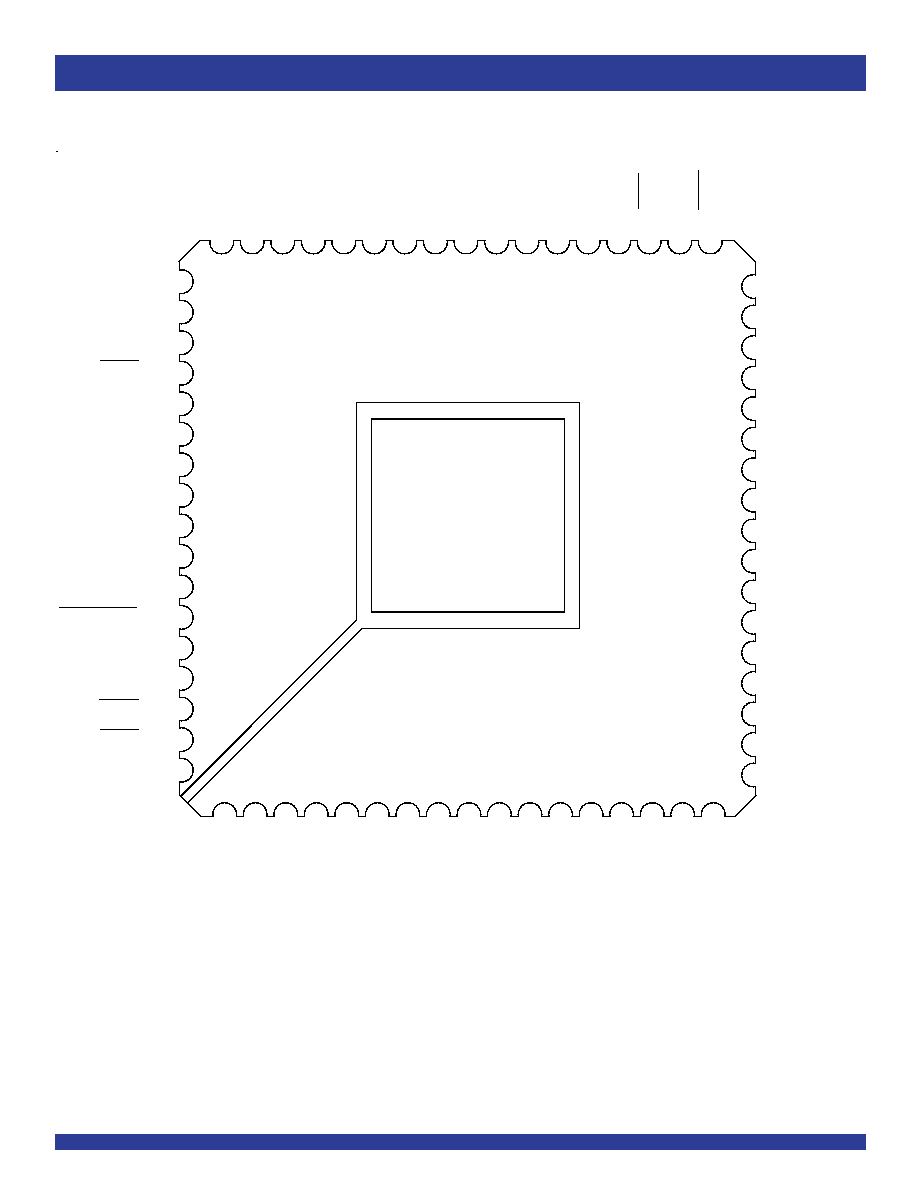
PIN CONFIGURATION
PLCC
TOP VIEW
J68-1
P
1
,Y
1
P
0
,Y
0
P
2
,Y
2
P
3
,Y
3
P
4
,Y
4
P
5
,Y
5
P
6
,Y
6
P
7
,Y
7
P
8
,Y
8
P
9
,Y
9
P
10
,Y
10
P
11
,Y
11
P
12
,Y
12
P
13
,Y
13
P
14
,Y
14
P
15
,Y
15
NC
X
0
X
1
X
2
X
3
X
4
X
5
X
6
X
7
X
8
X
9
X
1
0
X
1
2
X
1
1
N
C
O
E
L
C
L
K
E
N
Y
61
62
63
64
65
66
67
68
1
2
3
4
5
6
7
8
9
43
42
41
40
39
38
37
36
35
34
33
32
31
30
29
28
27
60
59
58
57
56
55
54
53
52
51
50
49
48
47
46
45
44
10
11
12
13
14
15
16
17
18
19
20
21
22
23
24
25
26
X
15
RND
ENX
Vcc
Vcc
P
1
,
P
1
7
P
0
,
P
1
6
P
2
,
P
1
8
P
3
,
P
1
9
P
4
,
P
2
0
P
5
,
P
2
1
P
6
,
P
2
2
P
7
,
P
2
3
P
8
,
P
2
4
P
9
,
P
2
5
P
1
0
,
P
2
6
P
1
1
,
P
2
7
P
1
2
,
P
2
8
P
1
3
,
P
2
9
P
1
4
,
P
3
0
P
1
5
,
P
3
1
N
C
X
14
X
13
X
M
Y
M
G ND
G ND
M SPSEL
FT
FA
OEP
ENP
NC

3
COMMERCIAL TEMPERATURE RANGE
IDT7217L
16 x 16 PARALLEL CMOS MULTIPLIERS
Symbol
Description
Max
Unit
V
CC
Power Supply Voltage
≠0.5 to +7
V
V
TERM
Terminal Voltage with Respect to GND
V
CC
+ 0.5
V
T
A
Operating Temperature
0 to +70
∞C
T
BIAS
Temperature Under Bias
≠55 to +125
∞C
T
STG
Storage Temperature
≠55 to +125
∞C
I
OUT
DC Output Current
50
mA
ABSOLUTE MAXIMUM RATINGS
(1)
NOTE:
1. Stresses greater than those listed under ABSOLUTE MAXIMUM RATINGS may cause
permanent damage to the device. This is a stress rating only and functional operation
of the device at these or any other conditions above those indicated in the operational
sections of this specification is not implied. Exposure to absolute maximum rating
conditions for extended periods may affect reliability.
Symbol
Parameter
(1)
Conditions
Max.
Unit
C
IN
Input Capacitance
V
IN
= 0V
10
pF
C
OUT
Output Capacitance
V
OUT
= 0V
12
pF
CAPACITANCE
(T
A
= +25∞C, F = 1.0MHz)
NOTE:
1. This parameter is sampled and not 100% tested.
PIN DESCRIPTION
Pin Name
I/O
Description
X
0
- X
15
I
Data Inputs
Y
0 -
Y
15
/
I/O
Y
0 -
Y
15
are data inputs
P
0
- P
15
P
0
- P
15
are LSP register output, enabled when OEL = 0
P
16
- P
31
O
Data Output (LSP or MSP)
OEL
I
Output enable control for LSP (least significant product). When LOW enables P
0
- P
15
. When HIGH P
0
- P
15
tristated.
OEP
I
Output enable control for MSP (most significant product). When LOW enables P
16
- P
31.
When HIGH P
16
- P
31
tristated.
X
M,
Y
M
I
Mode control for each data word. LOW designates unsigned data input and HIGH designates two's complement.
RND
I
"Round" control for rounding of MSP. When HIGH, 1 is added to the most significant bit of LSP. This signal is affected by the state of FA pin. When
FA = 1 and RND = 1, 1 is added to the 2
-15
bit (P
15
). When RND = 1 and FA = 0, 1 is added to the 2
-16
bit (P
14
). The RND input is registered.
It is clocked on the rising edge of CLK. Rounding always occurs in the positive direction which may introduce a systematic bias.
MSPSEL
I
When LOW, MSP is output on P
16
- P
31
lines. When HIGH, LSP is output on P
16
- P
31.
FA
I
Format adjust control. When HIGH, a full 32 bit product is selected. When LOW, a left shifted 31 bit product is selected with the sign bit replicated
in the LSP. FA is normally HIGH, except for certain fractional two's complement applications (see multiplier input / output formats).
FT
I
Flow through control. When HIGH, both MSP and LSP registers are by-passed.
CLK
I
X, Y, RND, LSP, and MSP register clock input
ENX
I
X register clock enable. Also enables RND register clock.
ENY
I
Y register clock enable. Also enables RND register clock.

4
COMMERCIAL TEMPERATURE RANGE
IDT7217L
16 x 16 PARALLEL CMOS MULTIPLIERS
Symbol
Parameter
Test Conditions
(1)
Min.
Typ.
(1)
Max.
Unit
V
IH
Input HIGH Voltage
Guaranteed Logic HIGH Level
2
--
--
V
V
IL
Input LOW Voltage
Guaranteed Logic LOW Level
--
--
0.8
V
I
LI
Input Leakage Current
V
CC
= Max., V
IN
= 0 to V
CC
--
--
10
µA
I
LO
Output Leakage Current
V
CC
= Max., OE = 2V, V
OUT
= 0 to V
CC
--
--
10
µA
I
CC
Operating Power Supply Current
V
CC
= Max., Outputs Disabled, f = 10MHz
(2)
--
40
80
mA
I
CCQ1
Quiescent Power Supply Current
V
IN
V
IH,
V
IN
V
IL
--
20
40
mA
I
CCQ2
Quiescent Power Supply Current
V
IN
V
CC
- 0.2V, V
IN
0.2V
--
4
20
mA
I
CC
/f
(2,3)
Increase in Power Supply Current
V
CC
= Max., Outputs Disabled
--
--
4
mA/MHz
V
OH
Output HIGH Voltage
V
CC
= Min., I
OH
= ≠2mA
2.4
--
--
V
V
OL(4)
Output LOW Voltage
V
CC
= Min., I
OL
= 8mA
--
--
0.4
V
I
OS
Output Short Circuit Current
V
CC
= Max., V
O
= GND
-20
--
-120
mA
DC ELECTRICAL CHARACTERISTICS OVER OPERATING RANGE
Following Conditions Apply Unless Otherwise Specified:
Commercial: T
A
= 0∞C to +70∞C, V
CC
= 5V ± 10%
AC ELECTRICAL CHARACTERISTICS
Following Conditions Apply Unless Otherwise Specified:
Commercial: T
A
= 0∞C to +70∞C, V
CC
= 5V ± 10%
7217L16
7217L20
7217L25
7217L35
Symbol
Parameter
Min.
Max.
Min.
Max.
Min.
Max.
Min.
Max.
Unit
t
MUC
Unclocked Multiply Time
(4)
2
25
2
30
2
38
2
55
ns
t
MC
Clocked Multiply Time
(4)
2
16
2
20
2
25
2
35
ns
t
S
X, Y, RND Set-up Time
10
--
11
--
12
--
12
--
ns
t
H
X, Y, RND Hold Time
1
--
1
--
2
--
3
--
ns
t
PWH
Clock Pulse Width HIGH
7
--
9
--
10
--
10
--
ns
t
PWL
Clock Pulse Width LOW
7
--
9
--
10
--
10
--
ns
t
PDSEL
MSPSEL to Product Out
(4)
2
15
2
18
2
20
2
25
ns
t
PDP
Output Clock to P
(4)
2
15
2
18
2
20
2
25
ns
t
PDY
Output Clock to Y
(4)
2
15
2
18
2
20
2
25
ns
t
ENA
3-State Enable Time
--
15
--
18
--
20
--
25
ns
t
DIS
3-State Disable Time
(2)
--
15
--
18
--
20
--
22
ns
t
S
Clock Enable Set-Up Time
9
--
10
--
10
--
10
--
ns
t
H
Clock Enable Hold Time
0
--
0
--
2
--
3
--
ns
NOTES:
1. To ensure that the correct product is entered in the output registers, new data may not be entered into the registers before the output registers have been clocked.
2. Transition is measured ±500mV from steady state voltage.
3. Guaranteed by design, not production tested.
4. Minimum propagation delay times are guaranteed, not production tested.
NOTES:
1. Typical implies V
CC
= 5V and T
A
= +25∞C.
2. I
CC
is measured at 10MHz and V
IN
= 0 to 3V. For frequencies greater than 10MHz, the following equation is used: I
CC
= 80+ 4(f ≠10)mA. f = operating frequency in MHz and
f = 1/t
MC
.
3. For frequencies greater than 10MHz, guaranteed by design, not production tested.
4. I
OL
= 4mA for t
MC
>65ns.

5
COMMERCIAL TEMPERATURE RANGE
IDT7217L
16 x 16 PARALLEL CMOS MULTIPLIERS
TIMING DIAGRAM
CLK
X
1
, Y
1
RND
t
H
t
S
t
PW L
OUTPUT Y
t
P D Y
M SPSEL
OUTPUT P
t
M C
t
PW H
t
PDSEL
t
PD P
t
M U C
ENP
t
S
t
H
ENX
ENY
t
H
t
S


