 | –≠–ª–µ–∫—Ç—Ä–æ–Ω–Ω—ã–π –∫–æ–º–ø–æ–Ω–µ–Ω—Ç: 72V71660 | –°–∫–∞—á–∞—Ç—å:  PDF PDF  ZIP ZIP |

1
2003 Integrated Device Technology, Inc. All rights reserved. Product specifications subject to change without notice.
DSC-5905/8
MAY 2003
PRELIMINARY
IDT72V71660
3.3 VOLT TIME SLOT INTERCHANGE
DIGITAL SWITCH
16,384
X
16,384
IDT and the IDT logo are registered trademarks of Integrated Device Technology, Inc. The ST-BUS
is a trademark of Mitel Corp.
FUNCTIONAL BLOCK DIAGRAM
FEATURES:
∑
∑
∑
∑
∑
16K x 16K non-blocking switching at 16.384Mb/s
∑
∑
∑
∑
∑
64 serial input and output streams
∑
∑
∑
∑
∑
Accepts data streams at 2.048Mb/s, 4.096Mb/s, 8.192Mb/s or
16.384Mb/s
∑
∑
∑
∑
∑
Per-channel Variable Delay Mode for low-latency applications
∑
∑
∑
∑
∑
Per-channel Constant Delay Mode for frame integrity applications
∑
∑
∑
∑
∑
Automatic identification of ST-BUS
Æ
and GCI bus interfaces
∑
∑
∑
∑
∑
Automatic frame offset delay measurement
∑
∑
∑
∑
∑
Per-stream frame delay offset programming
∑
∑
∑
∑
∑
Per-channel high-impedance output control
∑
∑
∑
∑
∑
Direct microprocessor access to all internal memories
∑
∑
∑
∑
∑
Memory block programming for quick setup
∑
∑
∑
∑
∑
IEEE-1149.1 (JTAG) Test Port
∑
∑
∑
∑
∑
3.3V Power Supply
∑
∑
∑
∑
∑
Available in 208-pin (17mm x 17mm) Plastic Ball Grid Array
(PBGA) and 208-pin (28mm x 28mm) Plastic Quad Flatpack
(PQFP) packages
∑
∑
∑
∑
∑
Operating Temperature Range -40
∞∞
∞∞
∞C to +85∞∞∞∞∞C
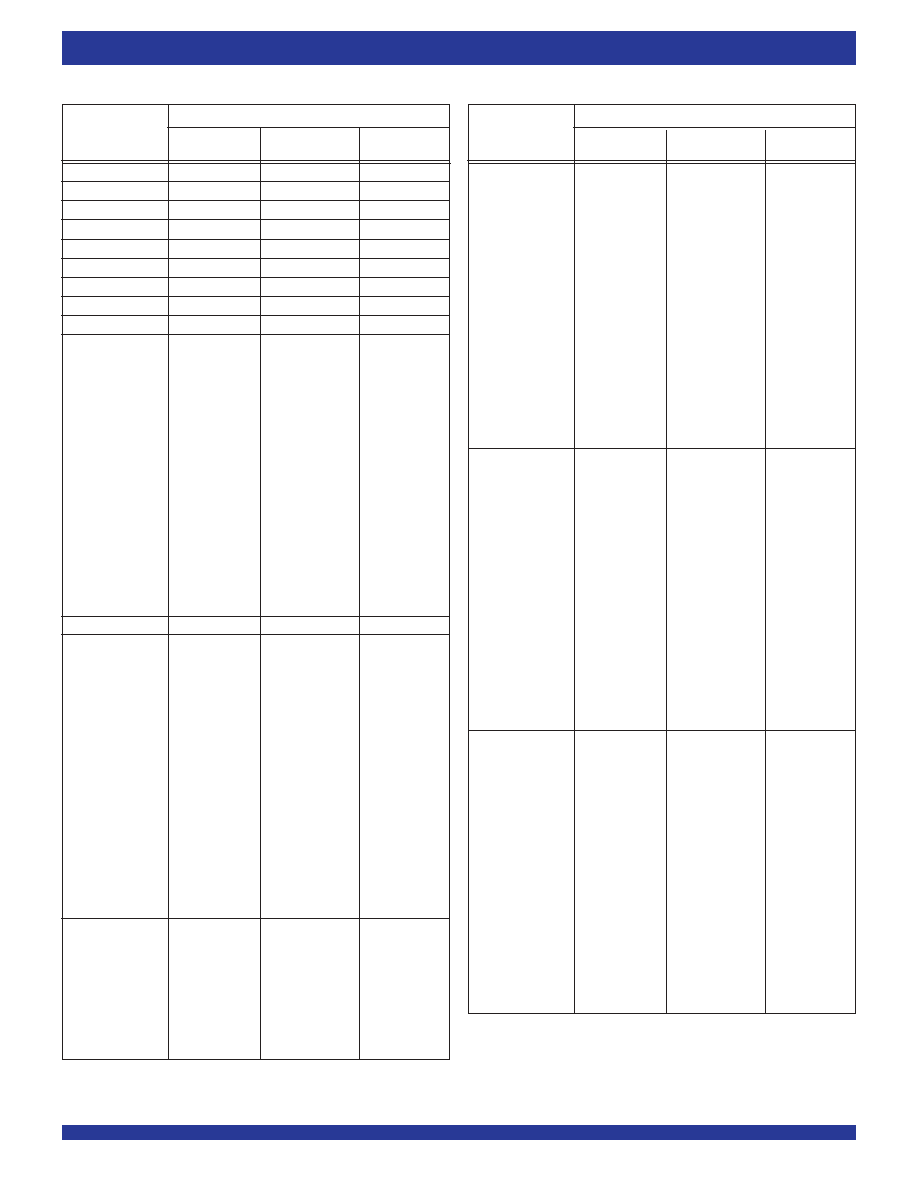
DESCRIPTION:
The IDT72V71660 has a non-blocking switch capacity of 2,048 x 2,048
channels at 2.048Mb/s, 4,096 x 4,096 channels at 4.096Mb/s, and 8,192 x
8,192 channels at 8.192Mb/s and 16,384 x 16,384 channels at 16.384Mb/s.
With 64 inputs and 64 outputs, programmable per stream control, and a variety
of operating modes the IDT72V71660 is designed for the TDM time slot
interchange function in either voice or data applications.
Some of the main features of the IDT72V71660 are LOW power 3.3 Volt
operation, automatic ST-BUS
Æ
/GCI sensing, memory block programming,
simple microprocessor interface, one cycle direct internal memory accesses,
JTAG Test Access Port (TAP) and per stream programmable input offset delay,
variable or constant throughput modes, output enable and processor mode.
The IDT72V71660 is capable of switching up to 16,384 x 16,384 channels
without blocking. Designed to switch 64 Kbit/s PCM or N x 64 Kbit/s data, the
device maintains frame integrity in data applications and minimizes throughput
delay for voice applications on a per-channel basis.
RX0
RX1
RX63
ODE
FP
V
CC
CS
R/
W
A0-A15
GND
DTA
D0-D15
TX0
TX1
TX3
1
TX63/OEI31
DS
CLK
FE/HCLK
RESET
5905 drw01
Receive
Serial Data
Streams
MUX
Data Memory
Internal
Registers
Microprocessor Interface
Timing Unit
Connection
Memory
Transmit
Serial Data
Streams
TX32/OEI0
TX33/OEI1
JTAG Port
WFPS
TDO
TMS TDI TCK
TRST

2
INDUSTRIAL TEMPERATURE RANGE
IDT72V71660 3.3V TIME SLOT INTERCHANGE
DIGITAL SWITCH 16,384 x 16,384
PBGA: 1mm pitch, 17mm x 17mm (BB208-1, order code: BB)
TOP VIEW
A
B
C
D
E
F
G
H
J
K
L
M
N
P
R
T
CLK
RESET
WFP
S
FP
CS
A2
A6
D3
D2
D1
D0
RX62
RX2
TX48/
OEI16
TX0
RX14
TX12
TX14
RX55
RX11
TX19
TX51/
OEI19
RX20
TX59/
OEI27
RX15
RX1
TX52/
OEI20
RX4
TX54/
OEI22
TX63/
OEI31
A12
RX59
TX16
TX18
TX20
TX25
TX28
RX24
1
2
3
4
5
6
7
8
9
10
11
12
13
14
15
16
A1 BALL PAD CORNER
TX27
TX30
RX26
RX29
RX30
RX33
GND
GND
GND
GND
GND
GND
GND
GND
GND
GND
GND
GND
GND
GND
GND
GND
TX8
RX5
A15
D14
D10
D7
RX60
RX61
TX15
RX10
TX33/
OEI1
RX37
A9
A14
D15
D12
D8
D5
TMS
TCK
R/
W
A3
A7
A10
DTA
A13
D13
D9
D6
D4
RX63
TX55/
OEI23
TX42/
OEI10
TX43/
OEI11
TX44/
OEI12
RX27
RX32
RX35
RX39
TX35/
OEI3
TX39/
OEI7
RX52
RX48
RX44
TX45/
OEI13
TX47/
OEI15
RX41
RX19
TX17
RX23
TRST
A0
A4
A8
A11
FE/HCLK
RX0
TX1
TX6
RX3
TX2
RX6
RX9
TX9
TX13
TX10
TX22
RX13
RX22
RX18
V
CC
DS
TX3
RX7
RX8
V
CC
V
CC
V
CC
TX24
RX12
RX21
RX17
V
CC
V
CC
RX36
TX32/
OEI0
TX36/
OEI4
RX43
RX42
RX16
TX31
V
CC
V
CC
RX58
TX58/
OEI26
TX62/
OEI30
RX53
RX45
RX49
RX40
TX46/
OEI14
RX31
RX34
RX38
TX34/
OEI2
TX38/
OEI6
TX41/
OEI9
TX26
TX29
RX25
RX28
A
1
A5
V
CC
V
CC
V
CC
V
CC
D11
NC
(1)
V
CC
RX56
TX56/
OEI24
TX60/
OEI28
RX51
V
CC
V
CC
V
CC
RX47
RX57
TX53/
OEI21
TX57/
OEI25
TX61/
OEI29
RX50
TX50/
OEI18
RX54
TX49/
OEI17
RX46
TX40/
OEI8
TX37/
OEI5
ODE
TX21
TX23
TDO
TX5
TX11
TX4
TX7
TDI
5905 drw02
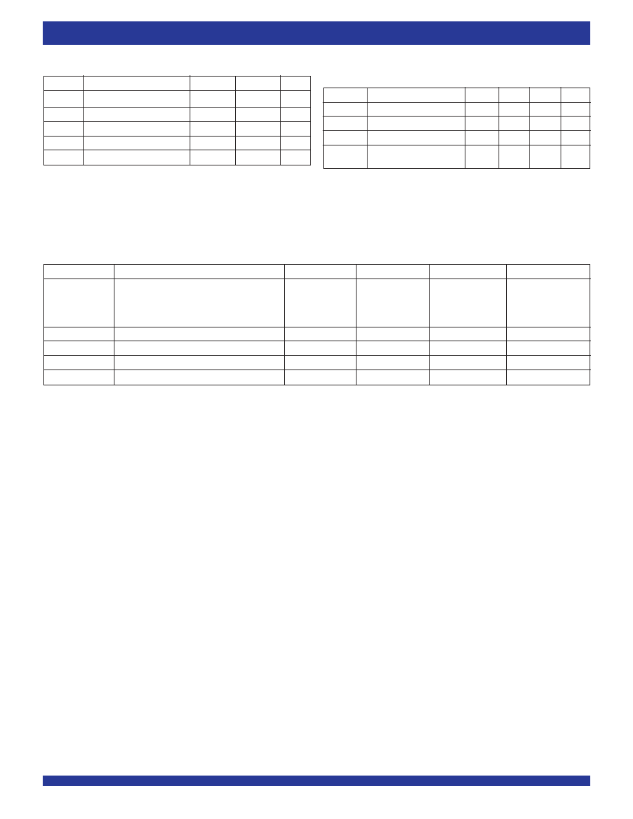
PIN CONFIGURATIONS
NOTE:
1. NC = No Connect

3
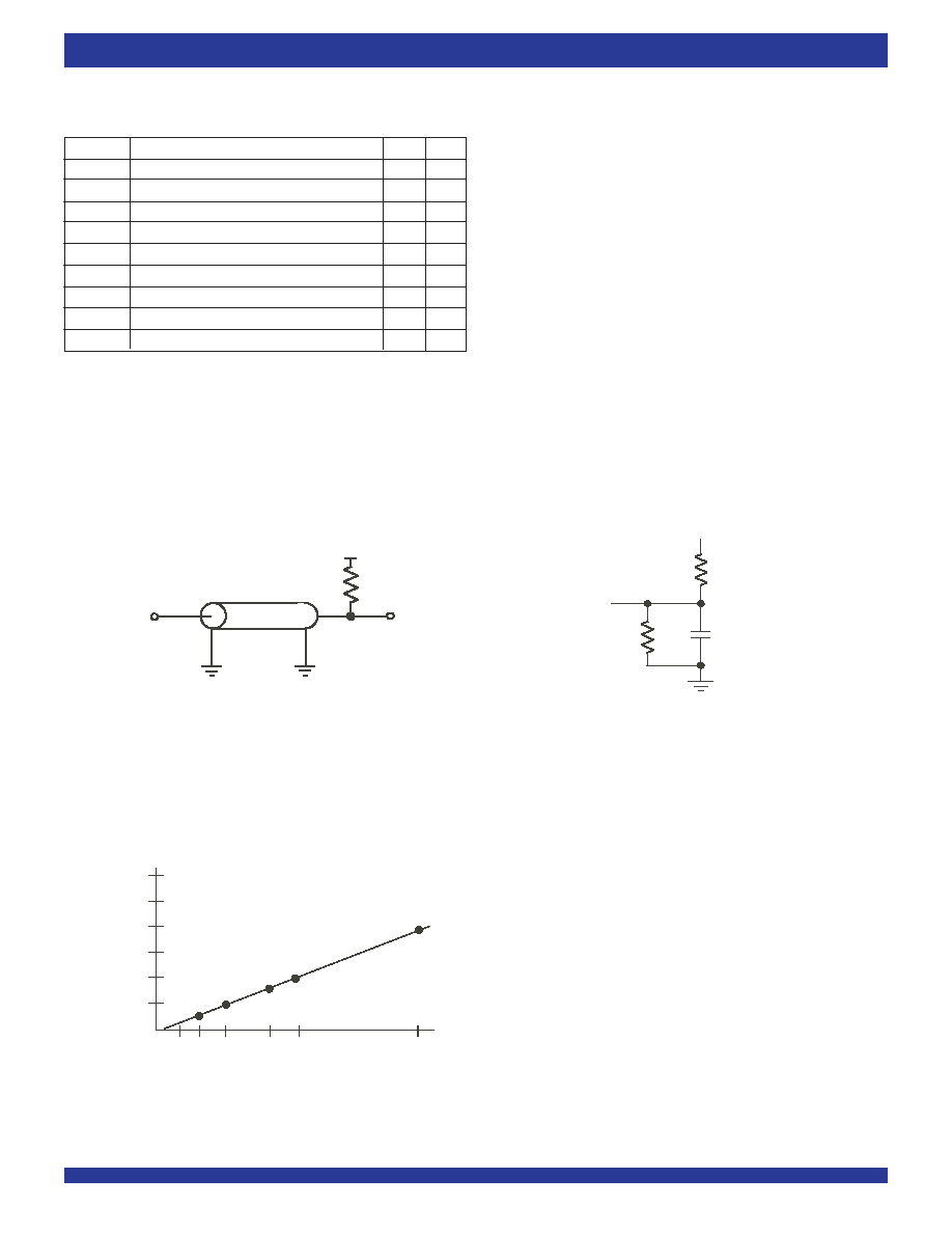
INDUSTRIAL TEMPERATURE RANGE
IDT72V71660 3.3V TIME SLOT INTERCHANGE
DIGITAL SWITCH 16,384 x 16,384
PIN CONFIGURATIONS (CONTINUED)
PQFP: 0.50mm pitch, 28mm x 28mm (DR208-1, order code: DR)
TOP VIEW
TX44/OEI12
TX45/OEI13
TX46/OEI14
TX47/OEI15
RX40
RX41
RX42
RX43
RX44
RX45
RX46
RX47
RX48
RX49
RX50
RX51
RX52
RX53
RX54
RX55
TX48/OEI16
TX49/OEI17
TX50/OEI18
TX51/OEI19
GND
V
CC
TX52/OEI20
TX53/OEI21
TX54/OEI22
TX55/OEI23
GND
V
CC
TX56/OEI24
TX57/OEI25
TX58/OEI26
TX59/OEI27
GND
V
CC
TX60/OEI28
TX61/OEI29
TX62/OEI30
TX63/OEI31
RX56
RX57
RX58
RX59
RX60
RX61
RX62
RX63
D0
D1
TX19
TX18
TX17
TX16
RX23
RX22
RX21
RX20
RX19
RX18
RX17
RX16
RX15
RX14
RX13
RX12
RX11
RX10
RX9
RX8
TX15
TX14
TX13
TX12
GND
V
CC
TX11
TX10
TX9
TX8
GND
V
CC
TX7
TX6
TX5
TX4
GND
V
CC
TX3
TX2
TX1
TX0
RX7
RX6
RX5
RX4
RX3
RX2
RX1
RX0
ODE
RESET
GND
CLK
FP
FE/HCLK
WFPS
TMS
TDI
TDO
TCK
TRST
DS
CS
R/
W
V
CC
A0
A1
A2
A3
A4
A5
A6
A7
A8
A9
A10
A11
A12
A13
A14
A15
NC
(1)
DTA
D15
D14
D13
D12
V
CC
GND
D11
D10
D9
D8
V
CC
GND
D7
D6
D5
D4
V
CC
GND
D3
D2
V
CC
GND
TX20
TX21
TX22
TX23
V
CC
GND
TX24
TX25
TX26
TX27
V
CC
GND
TX28
TX29
TX30
TX31
RX24
RX25
RX26
RX27
RX28
RX29
RX30
RX31
RX32
RX33
RX34
RX35
RX36
RX37
RX38
RX39
TX32/OEI0
TX33/OEI1
TX34/OEI2
TX35/OEI3
GND
V
CC
TX36/OEI4
TX37/OEI5
TX38/OEI6
TX39/OEI7
GND
V
CC
TX40/OEI8
TX41/OEI9
TX42/OEI10
TX43/OEI11
GND
V
CC
5905 drw03
1
2
3
4
5
6
7
8
9
10
11
12
13
14
15
16
17
18
19
20
21
22
23
24
25
26
27
28
29
30
31
32
33
34
35
36
37
38
39
40
41
42
43
44
45
46
47
48
49
50
51
52
156
155
154
153
152
151
150
149
148
147
146
145
144
143
142
141
140
139
138
137
136
135
134
133
132
131
130
129
128
127
126
125
124
123
122
121
120
119
118
117
116
115
114
113
112
111
110
109
108
107
106
105
∑
PIN
1
157
158
159
160
161
162
163
164
165
166
167
169
168
170
171
172
173
174
175
176
177
178
179
180
181
182
183
184
185
186
187
188
189
190
191
192
193
194
195
196
197
198
199
200
201
202
203
204
205
206
207
208
104
103
101
100
99
98
97
96
95
94
92
93
90
89
88
87
86
85
84
83
82
81
80
79
77
76
75
74
73
72
70
69
68
67
66
65
64
63
62
61
60
59
58
57
56
55
54
53
102
91
78
71
NOTE:
1. NC = No Connect

4
INDUSTRIAL TEMPERATURE RANGE
IDT72V71660 3.3V TIME SLOT INTERCHANGE
DIGITAL SWITCH 16,384 x 16,384
PIN DESCRIPTION
SYMBOL
NAME
I/O
DESCRIPTION
A0-15
Address 0 to 15
I
These address lines access all internal memories.
CLK
Clock
I
Serial clock for shifting data in/out on the serial data streams. Depending upon the value programmed, this
input accepts a 4.096, 8.192 or 16.384 MHz clock. See the Control Register bits on Table 5 for the values.
CS
Chip Select
I
This active LOW input is used by a microprocessor to activate the microprocessor port of IDT72V71660.
D0-15
Data Bus 0-15
I/O
These pins are the data bits of the microprocessor port.
DS
Data Strobe
I
This active LOW input works in conjunction with
CS to enable the read and write operations and enables the
data bus lines (D0-D15).
DTA
Data Transfer
O
Indicates that a data bus transfer is complete. When the bus cycle ends, this pin drives HIGH and then goes
Acknowledgment
high-impedance, allowing for faster bus cycles with a weaker pull-up resistor. A pull-up resistor is required
to hold a HIGH level when the pin is in high-impedance.
FE/HCLK Frame Evaluation/
I
When the WFPS pin is LOW, this pin is the frame measurement input. When the WFPS pin is HIGH, the
HCLK Clock
HCLK (4.096 MHZ clock) is required for frame alignment in the wide frame pulse mode (WFPS).
FP
Frame Pulse
I
When the WFPS pin is LOW, this input accepts and automatically identifies frame synchronization signals
formatted according to ST-BUS
Æ
and GCI specifications. When pin WFPS is HIGH, this pin accepts a
negative frame pulse, which conforms to the WFPS format.
GND
Ground
Ground Rail.
ODE
Output Drive Enable
I
This is the output enable control for the TX serial outputs. When the ODE input is LOW and the Output Stand
By bit of the Control Register is LOW, all TX outputs are in a high-impedance state. If this input is HIGH, the TX
output drivers are enabled. However, each channel may still be put into a high-impedance state by using the
per-channel control bit in the Connection Memory.
RESET
Device Reset
I
This input puts the IDT72V71660 into a reset state that clears the device internal counters, registers and
brings TX0-63 and D0-D15 into a high-impedance state. The
RESET pin must be held LOW for a
minimum of 20ns to properly reset the device.
R/
W
Read/Write
I
This input controls the direction of the data bus lines (D0-D15) during a microprocessor access.
RX0-63
Data Stream
I
Serial data input stream. These streams may have a data rate of 2.048Mb/s, 4.096Mb/s, 8.192Mb/s, or
Input 0 to 63
16.384Mb/s, depending upon the value programmed in the Control Register.
TCK
Test Clock
I
Provides the clock to the JTAG test logic.
TDI
Test Serial Data In
I
JTAG serial test instructions and data are shifted in on this pin. This pin is pulled HIGH by an internal pull-up
when not driven.
TDO
Test Serial Data Out
O
JTAG serial data is output on this pin on the falling edge of TCK. This pin is held in high-impedance state
when JTAG scan is not enabled.
TMS
Test Mode Select
I
JTAG signal that controls the state transitions of the Test Access Port controller. This pin is pulled HIGH by an
internal pull-up when not driven.
TRST
Test Reset
I
Asynchronously initializes the JTAG Test Access Port controller by putting it in the Test-Logic-Reset state. This
pin is pulled by an internal pull-up when not driven. This pin should be pulsed LOW on power-up, or held LOW,
to ensure that the IDT72V71660 is in the normal functional mode.
TX0-31
TX Output 0 to 31
O
Serial data output stream. These streams may have a data rate of 2.048Mb/s, 4.096Mb/s, 8.192Mb/s,
(Three-state Outputs)
or 16.384Mb/s, depending upon the value programmed in the Control Register.
TX32-63/ TX Output 32 to 63/
O
When all 64 output streams are selected via Control Register, these pins are the output streams TX32 to TX63
OEI0-31
Output Enable
and may operate at a data rate of 2.048Mb/s, 4.096Mb/s, 8.192Mb/s, or 16.384Mb/s. When output enable
Indication 0 to 31
function is selected, these pins reflect the active or high-impedance status for the
(Three-state Outputs)
corresponding output stream OEI0-31.
V
CC
V
CC
+3.3 Volt Power Supply.
WFPS
Wide Frame Pulse Select
I
When 1, enables the wide frame pulse (WFPS) Frame Alignment interface. When 0, the device operates in
ST-BUS
Æ
/GCI mode.

5
INDUSTRIAL TEMPERATURE RANGE
IDT72V71660 3.3V TIME SLOT INTERCHANGE
DIGITAL SWITCH 16,384 x 16,384
DESCRIPTION (CONTINUED)
The 64 serial input streams (RX) of the IDT72V71660 can run up to
16.384Mb/s allowing 256 channels per 125
µs frame. The data rates on the
output streams (TX) are identical to those on the input streams (RX).
With two main operating modes, Processor Mode and Connection Mode, the
IDT72V71660 can easily switch data from incoming serial streams (Data
Memory) or from the controlling microprocessor via Connection Memory. As
control and status information is critical in data transmission, the Processor Mode
is especially useful when there are multiple devices sharing the input and output
streams.
With data coming from multiple sources and through different paths, data
entering the device is often delayed. To handle this problem, the IDT72V71660
has a Frame Evaluation feature to allow individual streams to be offset from the
frame pulse in half clock-cycle intervals up to +7.5 clock cycles.
The IDT72V71660 also provides a JTAG Test Access Port, memory block
programming, a simple microprocessor interface and automatic ST-BUS
Æ
/GCI
sensing to shorten setup time, aid in debugging and ease use of the device
without sacrificing capabilities.
FUNCTIONAL DESCRIPTION
DATA AND CONNECTION MEMORY
All data that comes in through the RX inputs go through a serial-to-parallel
conversion before being stored into internal Data Memory. The 8 KHz frame
pulse (FP) is used to mark the 125
µs frame boundaries and to sequentially
address the input channels in Data Memory.
Data output on the TX streams may come from either the serial input streams
(Data Memory) or from the microprocessor (Connection Memory). In the case
that RX input data is to be output, the addresses in Connection Memory are used
to specify a stream and channel of the input. The Connection Memory is setup
in such a way that each location corresponds to an output channel for each
particular stream. In that way, more than one channel can output the same data.
In Processor Mode, the microprocessor writes data to the Connection Memory
locations corresponding to the stream and channel that is to be output. The lower
half (8 least significant bits) of the Connection Memory is output every frame until
the microprocessor changes the data or mode of the channel. By using this
Processor Mode capability, the microprocessor can access input and output
time-slots on a per-channel basis.
The two most significant bits of the Connection Memory are used to control
the per-channel mode of the out put streams. Specifically, the MOD1-0 bits are
used to select Processor Mode, Constant or Variable delay Mode, and the high-
impedance state of output drivers. If the MOD1-0 bits are set to 1-1 accordingly,
only that particular output channel (8 bits) will be in the high-impedance state.
If however, the ODE input pin is LOW and the Output Standby Bit in the Control
Register is LOW, all of the outputs will be in a high-impedance state even if a
particular channel in Connection Memory has enabled the output for that
channel. In other words, the ODE pin and Output Stand By control bit are master
output enables for the device (See Table 3).
SERIAL DATA INTERFACE TIMING
When a 16.384Mb/s serial data rate is required, the master clock frequency
will be running at 16.384 MHz resulting in a single-bit per clock. For all other
cases, 2.048Mb/s, 4.096Mb/s, and 8.192Mb/s, the master clock frequency will
be twice the data rate on the serial streams, resulting in two clocks per bit. Use
Table 5 to determine clock speed and the DR1-0 bits in the Control Register to
setup the device. The IDT72V71660 provides two different interface timing
modes, ST-BUS
Æ
or GCI. The IDT72V71660 automatically detects the pres-
ence of an input frame pulse and identifies it as either ST-BUS
Æ
or GCI.
In ST-BUS
Æ
, when running at 16.384 MHz, data is clocked out on the falling
edge and is clocked in on the subsequent rising-edge. At all other data rates,
there are two clock cycles per bit and every second falling edge of the master
clock marks a bit boundary and the data is clocked in on the rising edge of CLK,
three quarters of the way into the bit cell. See Figure 14 for timing.
In GCI format, when running at 16.384 MHz, data is clocked out on the rising
edge and is clocked in on the subsequent falling edge. At all other data rates,
there are two clock cycles per bit and every second rising edge of the master
clock marks the bit boundary and data is clocked in on the falling edge of CLK
at three quarters of the way into the bit cell. See Figure 15 for timing.
INPUT FRAME OFFSET SELECTION
Input frame offset selection allows the channel alignment of individual input
streams to be offset with respect to the output stream channel alignment . Although
all input data comes in at the same speed, delays can be caused by variable
path serial backplanes and variable path lengths which may be implemented
in large centralized and distributed switching systems. Because data is often
delayed, this feature is useful in compensating for the skew between input
streams.
Each input stream can have its own delay offset value by programming the
frame input offset registers (FOR, Table 8). The maximum allowable skew is +7.5
master clock (CLK) periods forward with a resolution of Ω clock period, see
Table 9. The output frame cannot be adjusted.
SERIAL INPUT FRAME ALIGNMENT EVALUATION
The IDT72V71660 provides the Frame Evaluation input to determine
different data input delays with respect to the frame pulse FP. A measurement
cycle is started by setting the Start Frame Evaluation bit of the Control Register
LOW for at least one frame. When the Start Frame Evaluation bit in the Control
Register is changed from LOW to HIGH, the evaluation starts. Two frames later,
the Complete Frame Evaluation bit of the Frame Alignment Register changes
from LOW to HIGH to signal that a valid offset measurement is ready to be read
from bits 0 to 11 of the Frame Alignment Register. The Start Frame Evaluation
bit must be set to zero before a new measurement cycle is started.
In ST-BUS
Æ
mode, the falling edge of the frame measurement signal (Frame
Evaluation) is evaluated against the falling edge of the ST-BUS
Æ
frame pulse.
In GCI mode, the rising edge of Frame Evaluation is evaluated against the rising
edge of the GCI frame pulse. See Table 7 and Figure 1 for the description of
the Frame Alignment Register.
MEMORY BLOCK PROGRAMMING
The IDT72V71660 provides users with the capability of initializing the entire
Connection Memory block in two frames. To set bits 14 and 15 of every
Connection Memory location, first program the desired pattern in the Block
Programming Data Bits (BPD 1-0), located in bits 7 and 8 of the Control Register.
The block programming mode is enabled by setting the Memory Block
Program bit of the Control Register HIGH. When the Block Programming Enable
bit of the Control Register is set to HIGH, the Block Programming Data will be
loaded into the bits 14 and 15 of every Connection Memory location. The other
Connection Memory bits (bit 0 to bit 13) are loaded with zeros. When the memory
block programming is complete, the device resets the Block Programming
Enable , BPD 1-0 and MBP bits to zero.

6
INDUSTRIAL TEMPERATURE RANGE
IDT72V71660 3.3V TIME SLOT INTERCHANGE
DIGITAL SWITCH 16,384 x 16,384
DELAY THROUGH THE IDT72V71660
The switching of information from the input serial streams to the output serial
streams results in a throughput delay. The device can be programmed to
perform time-slot interchange functions with different throughput delay capabili-
ties on a per-channel basis. For voice applications, variable throughput delay
is best as it ensure minimum delay between input and output data. In wideband
data applications, constant throughput delay is best as the frame integrity of the
information is maintained through the switch.
The delay through the device varies according to the type of throughput delay
selected in the Switching Mode Selection bits of the Connection Memory.
VARIABLE DELAY MODE (MOD1-0 = 0-0)
In this mode, the delay is dependent only on the combination of source and
destination channels and is independent of input and output streams. The
minimum delay achievable in the IDT72V71660 is three time-slots. If the input
channel data is switched to the same output channel (channel n, frame p), it will
be output in the following frame (channel n, frame p+1). The same is true if the
input channel n is switched to output channel n+1 or n+2. If the input channel
n is switched to output channel n+3, n+4,..., the new output data will appear in
the same frame. Table 2 shows the possible delays for the IDT72V71660 in
Variable Delay mode.
CONSTANT DELAY MODE (MOD1-0 = 0-1)
In this mode, frame integrity is maintained in all switching configurations by
making use of a multiple data memory buffer. Input channel data is written into
the data memory buffers during frame n will be read out during frame n+2. In
the IDT72V71660, the minimum throughput delay achievable in Constant Delay
mode will be one frame plus one channel. See Table 1.
MICROPROCESSOR INTERFACE
The IDT72V71660's microprocessor interface looks like a standard RAM
interface to improve integration into a system. With a 16-bit address bus and a
16-bit data bus, reads and writes are mapped directly into Data and Connection
Memories and require only one clock cycle to access. By allowing the internal
memories to be randomly accessed in one cycle, the controlling microprocessor
has more time to manage other peripheral devices and can more easily and
quickly gather information and setup the switch paths. Table 4 shows the
mapping of the addresses into internal memory blocks.
MEMORY MAPPING
The address bus on the microprocessor interface selects the internal registers
and memories of the IDT72V71660.
The two most significant bits of the address select between the registers, Data
Memory, and Connection Memory. If A15 and A14 are HIGH, A13-A0 are used
to address the Data Memory. If A15 is HIGH and A14 is LOW, A13-A0 are used
to address Connection Memory. If A15 is LOW and A14 is HIGH A13-A0 are
used to select the Control Register, Frame Alignment Register, and Frame Offset
Registers. See Table 4 for mappings.
As explained in the Serial Data Interface Timing and Switching Configurations
sections, after system power-up, the Control Register should be programmed
immediately to establish the desired switching configuration.
The data in the Control Register consists of the Memory Block Programming
bit, the Block Programming Data bits, the Begin Block Programming Enable, the
Output Stand By, Start Frame Evaluation, Output Enable Indication and Data
Rate Select bits. As explained in the Memory Block Programming section, the
Block Programming Enable begins the programming if the MBP bit is enabled.
This allows the entire Connection Memory block to be programmed with the
Block Programming Data bits. If the ODE pin is LOW, the Output Stand By bit
enables (if HIGH) or disables (if LOW) all TX output drivers. If the ODE pin is
HIGH, the Output Stand By bit is ignored and all TX output drivers are enabled.
SOFTWARE RESET
The Software Reset serves the same function as the hardware reset. As
with the hard reset, the Software Reset must also be set HIGH for 20ns before
bringing the Software Reset LOW again for normal operation. Once the Software
Reset is LOW, internal registers and other memories may be read or written.
During Software Reset, the microprocessor port is still able to read from all
internal memories. The only write operation allowed during a Software Reset
is to the Software Reset bit in the Control Register to complete the Software Reset.
CONNECTION MEMORY CONTROL
If the ODE pin and the Output Stand By bit are LOW, all output channels will
be in three-state. See Table 3 for detail.
If MOD1-0 of the Connection Memory is 1-0 accordingly, the output channel
will be in Processor Mode. In this case the lower eight bits of the Connection
Memory are output each frame until the MOD1-0 bits are changed. If MOD1-
0 of the Connection Memory are 0-1 accordingly, the channel will be in Constant
Delay Mode and bits 13-0 are used to address a location in Data Memory. If
MOD1-0 of the Connection Memory are 0-0, the channel will be in Variable
Delay Mode and bits 13-0 are used to address a location in Data Memory. If
MOD 1-0 of the Connection Memory are 1-1, the channel will be in high
Impedance mode and that channel will be in three-state.
OUTPUT ENABLE INDICATION
The IDT72V71660 has the capability to indicate the state of the outputs (active
or three-state) by enabling the Output Enable Indication in the Control Register.
In the Output Enable Indication mode however, only half of the output streams
are available. If this same capability is desired with all 64 streams, this can be
accomplished by using two IDT72V71660 devices. In one device, the All Output
Enable bit is set to a one while in the other the All Output Enable is set to zero.
In this way, one device acts as the switch and the other as a three-state control
device, see Figure 5. It is important to note if the TSI device is programmed for
All Output Enables and the Output Enable Indication is also set, the device will
be in the All Output Enables mode not Output Enable Indication. To use all 64
streams, set Output Enable Indication in the Control Register to zero.
INITIALIZATION OF THE IDT72V71660
After power up, the state of the Connection Memory is unknown. As such,
the outputs should be put in high-impedance by holding the ODE pin LOW. While
the ODE is LOW, the microprocessor can initialize the device by using the Block
Programming feature and program the active paths via the microprocessor bus.
Once the device is configured, the ODE pin (or Output Stand By bit depending
on initialization) can be switched to enable the TSI switch.
7
INDUSTRIAL TEMPERATURE RANGE
IDT72V71660 3.3V TIME SLOT INTERCHANGE
DIGITAL SWITCH 16,384 x 16,384
TABLE 4
-- INTERNAL REGISTER AND ADDRESS MEMORY MAPPING
TABLE 3
-- OUTPUT HIGH-IMPEDANCE CONTROL
TABLE 1
-- CONSTANT THROUGHPUT
DELAY VALUE
TABLE 2
-- VARIABLE THROUGHPUT
DELAY VALUE
NOTE: Unused STA and CH bits should be set to zero.
Delay for Constant Throughput Delay Mode
Input Rate
(m ≠ output channel number)
(n ≠ input channel number)
2.048Mb/s
32 + (32 ≠ n) +m time-slots
4.096Mb/s
64 + (64 ≠ n) +m time-slots
8.192Mb/s
128 + (128 ≠ n) +m time-slots
16.384Mb/s
256 + (256 ≠ n) +m time-slots
Delay for Variable Throughput Delay Mode
Input Rate
(m ≠ output channel number; n ≠ input channel number)
m
n+2
m > n+2
2.048Mb/s
32 ≠ (n-m) time-slots
(m-n) time-slots
4.096Mb/s
64 ≠ (n-m) time-slots
(m-n) time-slots
8.192Mb/s
128 ≠ (n-m) time-slots
(m-n) time-slots
16.384Mb/s
256 ≠ (n-m) time-slots
(m-n) time-slots
A15
A14
A13
A12
A11
A10
A9
A8
A7
A6
A5
A4
A3
A2
A1
A0
R/W
Location
1
1
STA5
STA4
STA3
STA2
STA1
STA0
CH7
CH6
CH5
CH4
CH3
CH2 CH1 CH0
R
Data Memory
1
0
STA5
STA4
STA3
STA2
STA1
STA0
CH7
CH6
CH5
CH4
CH3
CH2 CH1 CH0
R/W
Connection Memory
0
1
0
0
0
0
0
x
x
x
x
x
x
x
x
x
R/W
Control Register
0
1
0
0
0
0
1
x
x
x
x
x
x
x
x
x
R
Frame Align Register
0
1
1
0
0
0
0
x
x
x
x
x
x
x
x
x
R/W
Frame Offset Register 0
0
1
1
0
0
0
1
x
x
x
x
x
x
x
x
x
R/W
Frame Offset Register 1
0
1
1
0
0
1
0
x
x
x
x
x
x
x
x
x
R/W
Frame Offset Register 2
0
1
1
0
0
1
1
x
x
x
x
x
x
x
x
x
R/W
Frame Offset Register 3
0
1
1
0
1
0
0
x
x
x
x
x
x
x
x
x
R/W
Frame Offset Register 4
0
1
1
0
1
0
1
x
x
x
x
x
x
x
x
x
R/W
Frame Offset Register 5
0
1
1
0
1
1
0
x
x
x
x
x
x
x
x
x
R/W
Frame Offset Register 6
0
1
1
0
1
1
1
x
x
x
x
x
x
x
x
x
R/W
Frame Offset Register 7
0
1
1
1
0
0
0
x
x
x
x
x
x
x
x
x
R/W
Frame Offset Register 8
0
1
1
1
0
0
1
x
x
x
x
x
x
x
x
x
R/W
Frame Offset Register 9
0
1
1
1
0
1
0
x
x
x
x
x
x
x
x
x
R/W
Frame Offset Register 10
0
1
1
1
0
1
1
x
x
x
x
x
x
x
x
x
R/W
Frame Offset Register 11
0
1
1
1
1
0
0
x
x
x
x
x
x
x
x
x
R/W
Frame Offset Register 12
0
1
1
1
1
0
1
x
x
x
x
x
x
x
x
x
R/W
Frame Offset Register 13
0
1
1
1
1
1
0
x
x
x
x
x
x
x
x
x
R/W
Frame Offset Register 14
0
1
1
1
1
1
1
x
x
x
x
x
x
x
x
x
R/W
Frame Offset Register 15
Bits MOD1-0 Values in
ODE pin
OSB bit in Control
Output Status
Connection Memory
Register
1 and 1
Don't Care
Don't Care
Per-channel
high-Impedance
Any, other than 1 and 1
0
0
high-Impedance
Any, other than 1 and 1
0
1
Enable
Any, other than 1 and 1
1
0
Enable
Any, other than 1 and 1
1
1
Enable

8
INDUSTRIAL TEMPERATURE RANGE
IDT72V71660 3.3V TIME SLOT INTERCHANGE
DIGITAL SWITCH 16,384 x 16,384
TABLE 5
-- CONTROL REGISTER (CR) BITS
Reset Value:
0000
H
.
BIT
NAME
DESCRIPTION
15
SRS
A one will reset the device and have the same effect as the RESET pin. Must be zero for normal operation.
(Software Reset)
14
OEI
When 1, the TX32-63/OEI0-31 pins will be OEI0-31 and reflect the active or high-impedance state of their corresponding output data
(Output Enable Indication)
streams. When 0, this feature is disabled and these pins are used as output data streams TX32-63.
13
OEPOL
When 1, a one on an Output Enable Indication pin denotes an active state on the output data stream; zero on an Output Enable Indication
(Output Enable Polarity)
pin denotes high-impedance state. When 0, a one on an Output Enable Indication pin denotes high-impedance and a zero denotes
an active state.
12
AOE
When 1, TX0-63 will behave as OEI0-63 accordingly. These outputs will reflect the active or high-impedance state of the
(All Output Enables)
corresponding output data streams (TX0-63) in another IDT72V71660 if programmed identically. When 0, the TSI operates in the normal
switch mode.
11-10
Unused
Must be zero for normal operation.
9
MBP
When 1, the Connection Memory block programming feature is ready for the programming of Connection Memory HIGH bits,
(Memory Block Program)
bit 14 and bit 15. When 0, this feature is disabled.
8-7
BPD1-0
These bits carry the value to be loaded into the Connection Memory block whenever the memory block programming feature
(Block Programming
is activated. After the Memory Block Program bit in the Control Register is set to 1 and the Block Programming Enable is set to 1,
Data)
the contents of the bits Block Programming Data1-0 are loaded into bit 15 and 14 of the Connection Memory. Bit 13 to bit 0 of the
Connection Memory are set to 0.
6
BPE
A zero to one transition of this bit enables the memory block programming function. Once the Block Programming Enable
(Begin Block
bit is set HIGH, the device requires two frames to complete the block programming. After the programming function has finished,
Programming Enable)
the Block Programming Enable, Memory Block Program and Block Programming Data1-0 bits will be reset to zero by the device
to indicate the operation is complete.
5
OSB
When ODE = 0 and Output Stand By = 0, the output drivers of the transmit serial streams are in high-impedance mode. When
(Output Stand By)
either ODE = 1 or Output Stand By =1 the output serial streams drivers function normally.
4
SFE
A zero to one transition in this bit starts the Frame Evaluation procedure. When the Complete Frame Evaluation bit in the Frame Alignment
(Start Frame Evaluation)
Register changes from zero to one, the evaluation procedure stops. To start another Frame Evaluation cycle, set this bit to zero for
at least one frame.
3-2
Unused
Must be zero for normal operation.
1-0
DR1-0
DR1
DR0
Data Rate
Master Clock
(Data Rate Select)
0
0
2.048Mb/s
4.096 MHz
0
1
4.096Mb/s
8.192 MHz
1
0
8.192Mb/s
16.384 MHz
1
1
16.384Mb/s
16.384 MHz
15
14
13
12
11
10
9
8
7
6
5
4
3
2
1
0
SRS
OEI
OEPOL
AOE
0
0
MBP
BPD1
BPD0
BPE
OSB
SFE
0
0
DR1
DR0
9
INDUSTRIAL TEMPERATURE RANGE
IDT72V71660 3.3V TIME SLOT INTERCHANGE
DIGITAL SWITCH 16,384 x 16,384
TABLE 6
-- CONNECTION MEMORY BITS
NOTE:
1. Unused Source Stream Address Bits and Source Chan-
nel Address Bits bits should be set to zero.
15
14
13
12
11
10
9
8
7
6
5
4
3
2
1
0
MOD1
MOD0
SAB5
SAB4
SAB3
SAB2
SAB1
SAB0
CAB7
CAB6
CAB5
CAB4
CAB3
CAB2
CAB1
CAB0
Bit
Name
Description
15, 14 MOD1-0
MOD1 MOD0
MODE
(Switching Mode Selection)
0
0
Variable Delay mode
0
1
Constant Delay mode
1
0
Processor mode
1
1
Output high-impedance
13-8
SAB5-0
The binary value is the number of the data stream for the source of the connection.
(Source Stream Address Bits)
7-0
CAB7-0
The binary value is the number of the channel for the source of the connection.
(Source Channel Address Bits)

10
INDUSTRIAL TEMPERATURE RANGE
IDT72V71660 3.3V TIME SLOT INTERCHANGE
DIGITAL SWITCH 16,384 x 16,384
Figure 1. Example for Frame Alignment Measurement
TABLE 7
-- FRAME ALIGNMENT REGISTER (FAR) BITS
0
1
2
3
4
5
6
7
8
9
1
0
1
1
1
2
1
3
1
4
1
5
1
6
ST-BUS
Frame
CLK
Offset
Value
FE
Input
0
1
2
3
4
5
6
7
8
9
1
0
1
1
1
2
1
3
1
4
1
5
GCI
Frame
CLK
Offset
Value
FE
Input
(FD[10:0] = 06
H
)
(FD11 = 0, sample at CLK LOW
phase)
(FD[10:0] = 09
H
)
(FD11 = 1, sample at CLK HIGH
phase)
5905
drw04
Bit
Name
Description
15-13
Unused
Must be zero for normal operation
12
CFE (Complete
When Complete Frame Evaluation = 1, the Frame Evaluation is completed and bits FD11 to FD0 bits contains a valid frame alignment offset.
Frame Evaluation)
This bit is reset to zero, when Start Frame Evaluation bit in the Control Register is changed from 1 to 0.
11
FD11
The falling edge of Frame Evaluation (or rising edge for GCI mode) is sampled during the CLK-HIGH phase (FD11 = 1) or during the CLK-
(Frame Delay Bit 11) LOW phase (FD11 = 0). This bit allows the measurement resolution to Ω CLK cycle. This bit is reset to zero when the Start Frame Evaluation
bit of the Control Register changes from 1 to 0.
10-0
FD10-0
The binary value expressed in these bits refers to the measured input offset value. These bits are reset to zero when the Start Frame Evaluation
(Frame Delay Bits)
bit of the Control Register changes from 1 to 0. (FD10 ≠ MSB, FD0 ≠ LSB)
Reset Value:
0000
H
.
15
14
13
12
11
10
9
8
7
6
5
4
3
2
1
0
0
0
0
CFE
FD11
FD10
FD9
FD8
FD7
FD6
FD5
FD4
FD3
FD2
FD1
FD0

11
INDUSTRIAL TEMPERATURE RANGE
IDT72V71660 3.3V TIME SLOT INTERCHANGE
DIGITAL SWITCH 16,384 x 16,384
TABLE 8
-- FRAME INPUT OFFSET REGISTER (FOR) BITS
NOTE:
1. n denotes an input stream number from 0 to 63.
Reset Value:0000
H
for all FOR registers.
Register
15
14
13
12
11
10
9
8
7
6
5
4
3
2
1
0
FOR0 Register
OF32
OF31
OF30
DLE3
OF22
OF21
OF20
DLE2
OF12
OF11
OF10
DLE1
OF02
OF01
OF00
DLE0
FOR1 Register
OF72
OF71
OF70
DLE7
OF62
OF61
OF60
DLE6
OF52
OF51
OF50
DLE5
OF42
OF41
OF40
DLE4
FOR2 Register
OF112 OF111 OF110 DLE11 OF102 OF101 OF100 DLE10
OF92
OF91
OF90
DLE9
OF82
OF81
OF80
DLE8
FOR3 Register
OF152 OF151 OF150 DLE15 OF142 OF141 OF140 DLE14 OF132 OF131 OF130
DLE13 OF122 OF121 OF120 DLE12
FOR4 Register
OF192 OF191 OF190 DLE19 OF182 OF181 OF180 DLE18 OF172 OF171 OF170
DLE17 OD162 OD161 OF160 DLE16
FOR5 Register
OF232 OF231 OF230 DLE23 OF222 OF221 OF220 DLE22 OF212 OF211 OF210
DLE21 OF202 OF201 OF200 DLE20
FOR6 Register
OF272 OF271 OF270 DLE27 OF262 OF261 OF260 DLE26 OF252 OF251 OF250
DLE25 OF242 OF241 OF240 DLE24
FOR7 Register
OF312 OF311 OF310 DLE31 OF302 OF301 OF300 DLE30 OF292 OF291 OF290
DLE29 OF282 OF281 OF280 DLE28
FOR8 Register
OF352 OF351 OF350 DLE35 OF342 OF341 OF340 DLE34 OF332 OF331 OF330
DLE33 OF322 OF321 OF320 DLE32
FOR9 Register
OF392 OF391 OF390 DLE39 OF382 OF381 OF380 DLE38 OF372 OF371 OF370
DLE37 OF362 OF361 OF360 DLE36
FOR10 Register
OF432 OF431 OF430 DLE43 OF422 OF421 OF420 DLE42 OF412 OF411 OF410
DLE41 OF402 OF401 OF400 DLE40
FOR11 Register
OF472 OF471 OF470 DLE47 OF462 OF461 OF460 DLE46 OF452 OF451 OF450
DLE45 OF442 OF441 OF440 DLE44
FOR12 Register
OF512 OF511 OF510 DLE51 OF502 OF501 OF500 DLE50 OF492 OF491 OF490
DLE49 OF482 OF481 OF480 DLE48
FOR13 Register
OF552 OF551 OF550 DLE55 OF542 OF541 OF540 DLE54 OF532 OF531 OF530
DLE53 OF522 OF521 OF520 DLE52
FOR14 Register
OF592 OF591 OF590 DLE59 OF582 OF581 OF580 DLE58 OF572 OF571 OF570
DLE57 OF562 OF561 OF560 DLE56
FOR15 Register
OF632 OF631 OF630 DLE63 OF622 OF621 OF620 DLE62 OF612 OF611 OF610
DLE61 OF602 OF601 OF600 DLE60
Name
(1)
Description
OFn2, OFn1, OFn0
These three bits define how long the serial interface receiver takes to recognize and store bit 0 from the RX input pin: i.e., to start a new frame.
(Offset Bits 2, 1 & 0)
The input frame offset can be selected to +7.5 clock periods from the point where the external frame pulse input signal is applied to the FP
input of the device. See Figure 2.
DLEn
ST-BUS
Æ
and
DLEn = 0, offset is on the clock boundary
GCI mode:
DLEn = 1, offset is a half clock cycle off of the clock boundary.

12
INDUSTRIAL TEMPERATURE RANGE
IDT72V71660 3.3V TIME SLOT INTERCHANGE
DIGITAL SWITCH 16,384 x 16,384
Measurement Result from
Corresponding
Input Stream
Frame Delay Bits
Offset Bits
Offset
FD11
FD2
FD1
FD0
OFn2
OFn1
OFn0
DLEn
No clock period shift (Default)
1
0
0
0
0
0
0
0
+ 0.5 clock period shift
0
0
0
0
0
0
0
1
+ 1.0 clock period shift
1
0
0
1
0
0
1
0
+ 1.5 clock period shift
0
0
0
1
0
0
1
1
+ 2.0 clock period shift
1
0
1
0
0
1
0
0
+ 2.5 clock period shift
0
0
1
0
0
1
0
1
+ 3.0 clock period shift
1
0
1
1
0
1
1
0
+ 3.5 clock period shift
0
0
1
1
0
1
1
1
+ 4.0 clock period shift
1
1
0
0
1
0
0
0
+ 4.5 clock period shift
0
1
0
0
1
0
0
1
+5.0 clock period shift
1
1
0
1
1
0
1
0
+5.5 clock period shift
0
1
0
1
1
0
1
1
+6.0 clock period shift
1
1
1
0
1
1
0
0
+6.5 clock period shift
0
1
1
0
1
1
0
1
+7.0 clock period shift
1
1
1
1
1
1
1
0
+7.5 clock period shift
0
1
1
1
1
1
1
1
TABLE 9
-- OFFSET BITS (OFn2, OFn1, OFn0, DLEn) & FRAME DELAY BITS
(FD11, FD2-0)
Figure 2. Examples for Input Offset Delay Timing in 16.384Mb/s mode
FP (ST-BUS
)
RX Stream
(16.384 Mb/s)
5905 drw05
Bit 7
Bit 7
CLK
Bit 6
offset = 0, DLE = 0
offset = 1, DLE = 0
offset = 0, DLE = 1
FP (GCI)
Bit 0
Bit 0
offset = 0, DLE = 0
offset = 1, DLE = 0
offset = 0, DLE = 1
Bit 1
Bit 0
Bit 2
Bit 1
Bit 2
Bit 1
Bit 2
RX Stream
(16.384 Mb/s)
CLK
RX Stream
(16.384 Mb/s)
RX Stream
(16.384 Mb/s)
Bit 6
Bit 5
Bit 4
Bit 5
Bit 6
Bit 7
Bit 5
Bit 4
RX Stream
(16.384 Mb/s)
RX Stream
(16.384 Mb/s)

13
INDUSTRIAL TEMPERATURE RANGE
IDT72V71660 3.3V TIME SLOT INTERCHANGE
DIGITAL SWITCH 16,384 x 16,384
Figure 2. Examples for Input Offset Delay Timing in 8.192Mb/s, 4.096Mb/s and 2.048Mb/s mode (Continued)
FP (ST-BUS
)
RX Stream
5905 drw06
Bit 7
Bit 7
CLK
Bit 7
Bit 7
denotes the 3/4 point of the bit cell
offset = 0, DLE = 0
offset = 1, DLE = 0
offset = 0, DLE = 1
offset = 1, DLE = 1
FP (GCI)
Bit 0
Bit 0
CLK
Bit 0
Bit 0
denotes the 3/4 point of the bit cell
offset = 0, DLE = 0
offset = 1, DLE = 0
offset = 0, DLE = 1
offset = 1, DLE = 1
RX Stream
RX Stream
RX Stream
RX Stream
RX Stream
RX Stream
RX Stream
14
INDUSTRIAL TEMPERATURE RANGE
IDT72V71660 3.3V TIME SLOT INTERCHANGE
DIGITAL SWITCH 16,384 x 16,384
JTAG SUPPORT
The IDT72V71660 JTAG interface conforms to the Boundary-Scan standard
IEEE-1149.1. This standard specifies a design-for-testability technique called
Boundary-Scan test (BST). The operation of the boundary-scan circuitry is
controlled by an external Test Access Port (TAP) Controller.
TEST ACCESS PORT (TAP)
The Test Access Port (TAP) provides access to the test functions of the
IDT72V71660. It consists of three input pins and one output pin.
∑Test Clock Input (TCK)
TCK provides the clock for the test logic. The TCK does not interfere with any
on-chip clock and thus remains independent. The TCK permits shifting of test
data into or out of the Boundary-Scan register cells concurrently with the
operation of the device and without interfering with the on-chip logic.
∑Test Mode Select Input (TMS)
The logic signals received at the TMS input are interpreted by the Test Access
Port Controller to control the test operations. The TMS signals are sampled at
the rising edge of the TCK pulse. This pin is internally pulled to VCC when it is
not driven from an external source.
∑Test Data Input (TDI)
Serial input data applied to this port is fed either into the instruction register
or into a test data register, depending on the sequence previously applied to
the TMS input. Both registers are described in a subsequent section. The
received input data is sampled at the rising edge of TCK pulses. This pin is
internally pulled to VCC when it is not driven from an external source.
∑Test Data Output (TDO)
Depending on the sequence previously applied to the TMS input, the contents
of either the instruction register or data register are serially shifted out through
the TDO pin on the falling edge of each TCK pulse. When no data is shifted
through the boundary scan cells, the TDO driver is set to a high-impedance state.
∑Test Reset (TRST)
Reset the JTAG scan structure. This pin is internally pulled to VCC when it
is not driven from an external source.
INSTRUCTION REGISTER
In accordance with the IEEE-1149.1 standard, the IDT72V71660 uses public
instructions. The IDT72V71660 JTAG interface contains a four-bit instruction
register. Instructions are serially loaded into the instruction register from the TDI
when the Test Access Port Controller is in its shift-IR state. Subsequently, the
instructions are decoded to achieve two basic functions: to select the test data
register that may operate while the instruction is current, and to define the serial
test data register path, which is used to shift data between TDI and TDO during
data register scanning. See Table 12 below for Instruction decoding.
TEST DATA REGISTER
As specified in IEEE-1149.1, the IDT72V71660 JTAG Interface contains two
test data registers:
∑The Boundary-Scan register
The Boundary-Scan register consists of a series of Boundary-Scan cells
arranged to form a scan path around the boundary of the IDT72V71660 core
logic.
∑The Bypass Register
The Bypass register is a single stage shift register that provides a one-bit path
from TDI to TDO. The IDT72V71660 boundary scan register bits are shown
in Table 14. Bit 0 is the first bit clocked out. All three-state enable bits are active
HIGH.
ID CODE REGISTER
As specified in IEEE-1149.1, this instruction loads the IDR with the Revision
Number, Device ID, and ID Register Indicator Bit. See Table 10.
INSTRUCTION FIELD
VALUE
DESCRIPTION
Revision Number (31:28)
0x0
Reserved for version number
IDT Device ID (27:12)
0x434
Defines IDT part number
IDT JEDEC ID (11:1)
0x33
Allows unique identification of device vendor as IDT
ID Register Indicator Bit (Bit 0)
1
Indicates the presence of an ID register
TABLE 10
-- IDENTIFICATION REGISTER DEFINITIONS
REGISTER NAME
BIT SIZE
Instruction (IR)
4
Bypass (BYR)
1
Identification (IDR)
32
Boundary Scan (BSR)
Note(1)
TABLE 11
-- SCAN REGISTER SIZES
NOTE:
1. The Boundary Scan Descriptive Language (BSDL) file for this device is available on
the IDT website (www.idt.com), or by contacting your local IDT sales representative.
15
INDUSTRIAL TEMPERATURE RANGE
IDT72V71660 3.3V TIME SLOT INTERCHANGE
DIGITAL SWITCH 16,384 x 16,384
NOTES:
1. Device outputs = All device outputs except TDO.
2. Device inputs = All device inputs except TDI, TMS and
TRST.
TABLE 12
-- SYSTEM INTERFACE PARAMETERS
INSTRUCTION
CODE
DESCRIPTION
EXTEST
0000
Forces contents of the boundary scan cells onto the device outputs
(1)
. Places the boundary scan register (BSR) between TDI and TDO.
BYPASS
1111
Places the bypass register (BYR) between TDI and TDO.
IDCODE
0010
Loads the ID register (IDR) with the vendor ID code and places the register between TDI and TDO.
HIGH-Z
0100
Places the bypass register (BYR) between TDI and TDO. Forces all device output drivers to a High-Z state.
CLAMP
0011
Places the bypass register (BYR) between \TDI and TDO. Forces contents of the boundary scan cells onto the device outputs.
SAMPLE/PRELOAD
0001
Places the boundary scan register (BSR) between TDI and TDO. SAMPLE allows data from device inputs
(2)
and outputs
(1)
to
be captured in the boundary scan cells and shifted serially through TDO. PRELOAD allows data to be input serially into the boundary
scan cells via the TDI.
RESERVED
All other codes Several combinations are reserved. Do not use other codes than those identified above.
SYMBOL
PARAMETER
MIN.
MAX.
UNITS
t
JCYC
JTAG Clock Input Period
100
ns
t
JCH
JTAG Clock HIGH
40
ns
t
JCL
JTAG Clock LOW
40
ns
t
JR
JTAG Clock Rise Time
3
(1)
ns
t
JF
JTAG Clock Fall Time
3
(1)
ns
t
JRST
JTAG Reset
50
ns
t
JRSR
JTAG Reset Recovery
50
ns
t
JCD
JTAG Data Output
25
ns
t
JDC
JTAG Data Output Hold
0
ns
t
JS
JTAG Setup
15
ns
t
JH
JTAG Hold
15
ns
NOTES:
1. Guaranteed by design.
2. 30pF loading on external output signals.
3. Refer to AC Electrical Test Conditions stated earlier in this document.
4. JTAG operations occur at one speed (10MHz). The base device may run at any speed specified in this datasheet.
TABLE 13 -- JTAG AC ELECTRICAL CHARACTERISTICS
(1,2,3,4)
TCK
Device Inputs
(1)
TDI/TMS
t
JDC
t
JS
t
JRSR
t
JF
t
JR
x
t
JCL
t
JCYC
t
JCH
t
JH
t
JCD
t
JRST
Device Outputs
(2)
TDO
TRST
5905 drw07
Figure 3. JTAG TIming Specifications
NOTES:
1. Device inputs = All device inputs except TDI, TMS and
TRST.
2. Device outputs = All device outputs except TDO.
16
INDUSTRIAL TEMPERATURE RANGE
IDT72V71660 3.3V TIME SLOT INTERCHANGE
DIGITAL SWITCH 16,384 x 16,384
TABLE 14
-- BOUNDARY SCAN REGISTER BITS
Boundary Scan Bit 0 to bit 265
Device Pin
Input
Output
Three-State
Scan Cell
Scan Cell
Control
ODE
0
RESET
1
CLK
2
FP
3
FE/HCLK
4
WFPS
5
DS
6
CS
7
R/
W
8
A0
9
A1
10
A2
11
A3
12
A4
13
A5
14
A6
15
A7
16
A8
17
A9
18
A10
19
A11
20
A12
21
A13
22
A14
23
A15
24
DTA
25
D15
26
27
28
D14
29
30
31
D13
32
33
34
D12
35
36
37
D11
38
39
40
D10
41
42
43
D9
44
45
46
D8
47
48
49
D7
50
51
52
D6
53
54
55
D5
56
57
58
D4
59
60
61
D3
62
63
64
D2
65
66
67
D1
68
69
70
D0
71
72
73
RX63
74
RX62
75
RX61
76
RX60
77
RX59
78
RX58
79
RX57
80
RX56
81
TX63/OEI31
82
83
TX62/OEI30
84
85
TX61/OEI29
86
87
TX60/OEI28
88
89
TX59/OEI27
90
91
TX58/OEI26
92
93
TX57/OEI25
94
95
TX56/OEI24
96
97
TX55/OEi23
98
99
TX54/OEi22
100
101
TX53/OEI21
102
103
TX52/OEI20
104
105
TX51/OEI19
106
107
TX50/OEI18
108
109
TX49/OE17
110
111
TX48/OEI16
112
113
RX55
114
RX54
115
RX53
116
RX52
117
RX51
118
RX50
119
RX49
120
RX48
121
RX47
122
RX46
123
RX45
124
RX44
125
RX43
126
RX42
127
RX41
128
RX40
129
TX47/OEI15
130
131
TX46/OEI14
132
133
TX45/OEI13
134
135
TX44/OEI12
136
137
TX43/OEI11
138
139
TX42/OEI10
140
141
TX41/OEI9
142
143
TX40/OEI8
144
145
TX39/OEI7
146
147
TX38/OEI6
148
149
TX37/OEI5
150
151
TX36/OEI4
152
153
TX35/OEI3
154
155
TX34/OEI2
156
157
TX33/OEI1
158
159
TX32/OEI0
160
161
Boundary Scan Bit 0 to bit 265
Device Pin
Input
Output
Three-State
Scan Cell
Scan Cell
Control

17
INDUSTRIAL TEMPERATURE RANGE
IDT72V71660 3.3V TIME SLOT INTERCHANGE
DIGITAL SWITCH 16,384 x 16,384
TABLE 14
-- BOUNDARY SCAN REGISTER BITS (CONTINUED)
RX39
162
RX38
163
RX37
164
RX36
165
RX35
166
RX34
167
RX33
168
RX32
169
RX31
170
RX30
171
RX29
172
RX28
173
RX27
174
RX26
175
RX25
176
RX24
177
TX31
178
179
TX30
180
181
TX29
182
183
TX28
184
185
TX27
186
187
TX26
188
189
TX25
190
191
TX24
192
193
TX23
194
195
TX22
196
197
TX21
198
199
TX20
200
201
TX19
202
203
TX18
204
205
TX17
206
207
TX16
208
209
RX23
210
RX22
211
RX21
212
RX20
213
RX19
214
RX18
215
RX17
216
RX16
217
RX15
218
RX14
219
RX13
220
RX12
221
RX11
222
RX10
223
RX9
224
RX8
225
TX15
226
227
TX14
228
229
TX13
230
231
TX12
232
233
TX11
234
235
TX10
236
237
TX9
238
239
TX8
240
241
TX7
242
243
TX6
244
245
TX5
246
247
TX4
248
249
TX3
250
251
TX2
252
253
TX1
254
255
TX0
256
257
RX7
258
RX6
259
RX5
260
RX4
261
RX3
262
RX2
263
RX1
264
RX0
265
Boundary Scan Bit 0 to bit 265
Device Pin
Input
Output
Three-State
Scan Cell
Scan Cell
Control
Boundary Scan Bit 0 to bit 265
Device Pin
Input
Output
Three-State
Scan Cell
Scan Cell
Control

18
INDUSTRIAL TEMPERATURE RANGE
IDT72V71660 3.3V TIME SLOT INTERCHANGE
DIGITAL SWITCH 16,384 x 16,384
Device 1
IDT72V71660
Device 2
IDT72V71660
Device 3
IDT72V71660
Device 4
IDT72V71660
RX0-63
RX64-127
TX0-63
TX64-127
5905 drw08
APPLICATIONS
CREATING LARGE SWITCH MATRICES
To create a switch matrix with twice the capacity of a given TSI device, four
devices must be used. In the example below, four IDT72V71660, 16K x 16K
channel capacity devices are used to create a 32K x 32K channel switch matrix.
As can be seen, Device #1 and Device #2 will receive the same incoming
RX0-63 data and thus have the same contents in Data Memory. On the output
side, however Device #1 is used to switch data out on to TX0-63 where as
Device #2 is used to switch out on TX 64-127. Likewise Device #3 and
Device #4 are used in the same way as Device #1 and Device #2 but
switch RX 64-127 to TX0-63 and TX 64-127, respectively. With this configu-
ration all possible combinations of input and output streams are possible. In short,
Device #1 is used to switch RX0-63 to TX0-63, Device #2 to switch RX0-63
to TX64-127, Device #3 to switch RX 64-127 to TX0-63, and Device #4 to switch
RX64-127 to TX64-127.
Figure 4. Creating Larger Switch Matrices

19
INDUSTRIAL TEMPERATURE RANGE
IDT72V71660 3.3V TIME SLOT INTERCHANGE
DIGITAL SWITCH 16,384 x 16,384
RX0-31
RX32-63
TX0-31
TX32-63
5905 drw09
OEI0-31
OEI32-63
TX0-31
RX0-31
OEI0-31
TX0-31
RX0-31
TX0-31
RX0-31
OEI0-31
TX0-31
RX0-31
TX0
RX0
RX63
TX63
OEI0
OEI63
RX32-63
RX32-63
RX32-63
RX32-63
TX32-63
TX32-63
RX0
RX63
RX0
RX63
RX0
RX63
Using OEI
Using AOE
AOE=0
AOE=0
AOE=0
AOE=0
AOE=0
AOE=1
TX0
TX63
TX0
TX63
OEI =1
OEI =0
OEI =1
OEI =0
OEI =0
OEI =0
Figure 5. Using All Output Enable (AOE)
20
INDUSTRIAL TEMPERATURE RANGE
IDT72V71660 3.3V TIME SLOT INTERCHANGE
DIGITAL SWITCH 16,384 x 16,384
Symbol
Parameter
Min.
Typ.
Max.
Units
I
CC
(2)
Supply Current
@ 2.048Mb/s
-
-
80
mA
@ 4.096Mb/s
-
-
90
mA
@ 8.192Mb/s
-
-
130
mA
@ 16.384Mb/s
-
-
140
mA
I
IL
(3,4)
Input Leakage (input pins)
-
-
60
µA
I
OZ
(3,4)
high-impedance Leakage
-
-
60
µA
V
OH
(5)
Output HIGH Voltage
2.4
-
-
V
V
OL
(6)
Output LOW Voltage
-
-
0.4
V
DC ELECTRICAL CHARACTERISTICS
NOTES:
1. Voltages are with respect to ground (GND) unless otherwise stated.
2. Outputs unloaded.
3. 0
V V
CC
.
4. Maximum leakage on pins (output or I/O pins in high-impedance state) is over an applied voltage (V).
5. IOH = 10 mA.
6. IOL = 10 mA.
Symbol
Parameter
Min.
Max.
Unit
V
CC
Supply Voltage
-0.5
+4.0
V
Vi
Voltage on Digital Inputs
GND -0.3
V
CC
+0.3
V
I
O
Current at Digital Outputs
-50
50
mA
T
S
Storage Temperature
-55
+125
∞ C
P
D
Package Power Dissapation
2
W
NOTE:
1. Exceeding these values may cause permanent damage. Functional operation under
these conditions is not implied.
ABSOLUTE MAXIMUM RATINGS
(1)
RECOMMENDED OPERATING
CONDITIONS
(1)
NOTE:
1. Voltages are with respect to Ground unless otherwise stated.
Symbol
Parameter
Min.
Typ.
Max.
Unit
V
CC
Positive Supply
3.0
3.3
3.6
V
V
IH
Input HIGH Voltage
2.0
V
CC
V
V
IL
Input LOW Voltage
-0.3
0.8
V
T
OP
Operating Temperature
-40
25
+85
∞C
Industrial
21
INDUSTRIAL TEMPERATURE RANGE
IDT72V71660 3.3V TIME SLOT INTERCHANGE
DIGITAL SWITCH 16,384 x 16,384
Symbol
Rating
Level
Unit
V
TT
TTL Threshold
1.5
V
V
HM
TTL Rise/Fall Threshold Voltage HIGH
2.0
V
V
LM
TTL Rise/Fall Threshold Voltage LOW
0.8
V
Input Pulse Levels
V
tr,tf
Input Rise/Fall Times
1
ns
Input Timing Reference Levels
V
Output Reference Levels
V
C
L
(1)
Output Load
150
pF
Cin
(2)
Input Capacitance
8
pF
AC ELECTRICAL CHARACTERISTICS - TIMING PARAMETER
MEASUREMENT VOLTAGE LEVELS
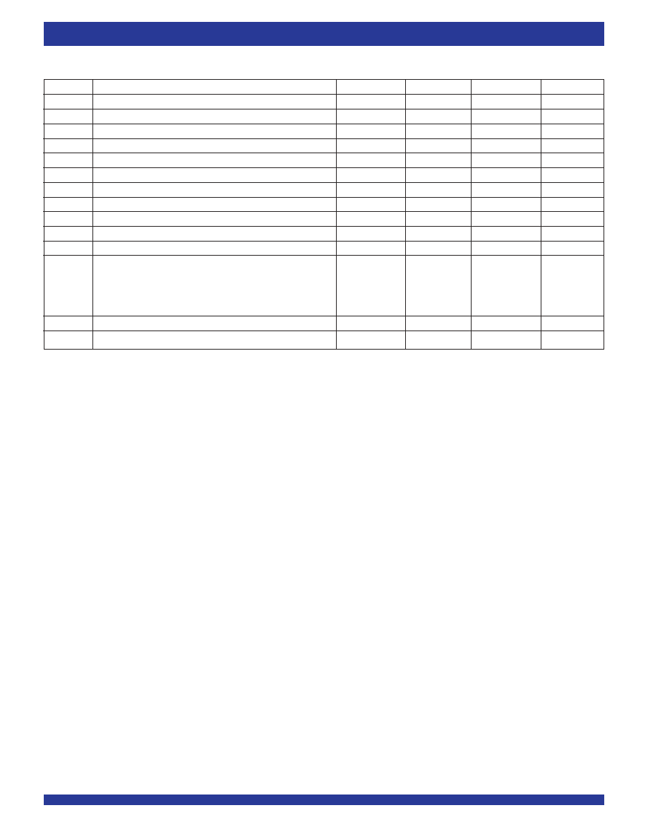
Figure 6. AC Termination
5905 drw12
6
5
4
3
2
1
20 30 50
80 100
200
Capacitance (pF)
t
SOD
(Typical, ns)
Figure 8. Lumped Capacitive Load, Typical Derating
Not Yet Characterized
NOTES:
1. JTAG C
L
is 30pF
2. For 208 PQFP.
5905 drw10
50
V
DD
I/O
Z0 = 50
5905 Drw11
330
30pF*
510
3.3v
D.U.T.
Figure 7. AC Test Load

22
INDUSTRIAL TEMPERATURE RANGE
IDT72V71660 3.3V TIME SLOT INTERCHANGE
DIGITAL SWITCH 16,384 x 16,384
AC ELECTRICAL CHARACTERISTICS - FRAME PULSE AND CLOCK
Symbol
Parameter
Min.
Typ.
Max.
Units
t
FPW
Frame Pulse Width (ST-BUS
Æ
, GCI)
Bit rate = 2.048Mb/s
26
295
ns
Bit rate = 4.096Mb/s
26
145
ns
Bit rate = 8.192Mb/s or 16.384Mb/s
26
65
ns
t
FPS
Frame Pulse Setup time before CLK falling (ST-BUS
Æ
or GCI)
5
ns
t
FPH
Frame Pulse Hold Time from CLK falling (ST-BUS
Æ
or GCI)
10
ns
t
CP
CLK Period
Bit rate = 2.048Mb/s
190
244
300
ns
Bit rate = 4.096Mb/s
110
122
150
ns
Bit rate = 8.192Mb/s or 16.384Mb/s
55
61
70
ns
t
CH
CLK Pulse Width HIGH
Bit rate = 2.048Mb/s
85
122
150
ns
Bit rate = 4.096Mb/s
50
61
75
ns
Bit rate = 8.192Mb/s or 16.384Mb/s
20
30
40
ns
t
CL
CLK Pulse Width LOW
Bit rate = 2.048Mb/s
85
122
150
ns
Bit rate = 4.096Mb/s
50
61
75
ns
Bit rate = 8.192Mb/s or 16.384Mb/s
20
30
40
ns
t
HFPW
Wide Frame Pulse Width
HCLK = 4.096Mb/s
244
ns
t
HFPS
Frame Pulse Setup Time before HCLK @ 4.096 MHz falling
50
150
ns
t
HFPH
Frame Pulse Hold Time from HCLK @ 4.096 MHz falling
50
150
ns
t
HCP
HCLK Period
@ 4.096 MHz
190
244
300
ns
t
HCH
HCLK Pulse Width HIGH
@ 4.096Mb/s
110
122
150
ns
t
HCL
HCLK Pulse Width LOW
@ 4.096Mb/s
110
122
150
ns
t
Hr
, t
Hf
HCLK Rise/Fall Time
10
ns
t
DIF
Delay between falling edge of HCLK and falling edge of CLK
-10
10
ns

23
INDUSTRIAL TEMPERATURE RANGE
IDT72V71660 3.3V TIME SLOT INTERCHANGE
DIGITAL SWITCH 16,384 x 16,384
Figure 10. Serial Output and External Control
Figure 11. Output Driver Enable (ODE)
C32i
(ST-BUS
mode)
TX
TX
VALID DATA
VALID DATA
C32i
(GCI mode)
5905 drw14
t
CHZ
t
CLZ
t
SOD
t
SIH
ODE
TX
VALID DATA
5905 drw15
t
ODEL
Z
t
ODEHZ
t
ODEA
RESET
TX
ODE
t
RS
t
ZR
t
RZ
t
RZ
t
ODELZ
5905 drw13
t
ODE(1)
Figure 9. RESET and ODE Timing
NOTE:
1. To guarentee TX outputs remain in high-impedance.
24
INDUSTRIAL TEMPERATURE RANGE
IDT72V71660 3.3V TIME SLOT INTERCHANGE
DIGITAL SWITCH 16,384 x 16,384
AC ELECTRICAL CHARACTERISTICS - MICROPROCESSOR INTERFACE TIMING
Symbol
Parameter
Min.
Typ.
Max.
Units
t
CSS
CS Setup from DS falling
0
ns
t
RWS
R/W Setup from DS falling
3
ns
t
ADS
Address Setup from DS falling
2
ns
t
CSH
CS Hold after DS rising
0
ns
t
RWH
R/W Hold after DS Rising
3
ns
t
ADH
Address Hold after DS Rising
2
ns
t
DDR
Data Setup from
DTA LOW on Read
1
ns
t
DHR
Data Hold on Read
10
15
25
ns
t
DSW
Data Setup on Write (Register Write)
10
ns
t
SWD
Valid Data Delay on Write (Connection Memory Write)
0
ns
t
DHW
Data Hold on Write
5
ns
t
AKD
Acknowledgment Delay:
Reading/Writing Registers
32
ns
Reading/Writing Memory
@
2.048Mb/s
345
ns
@
4.096Mb/s
200
ns
@
8.192Mb/s or 16.384Mb/s
120
ns
t
AKH
Acknowledgment Hold Time
20
ns
t
DSS
Data Strobe Setup Time
6
ns

25
INDUSTRIAL TEMPERATURE RANGE
IDT72V71660 3.3V TIME SLOT INTERCHANGE
DIGITAL SWITCH 16,384 x 16,384
DS
5905 drw16
VALID WRITE DATA
D0-D15
READ
CS
DTA
VALID READ DATA
VALID ADDRESS
t
AKH
D0-D15
WRITE
R/
W
A0-A11
CLK GCI
CLK ST-BUS
t
DDR
t
AKD
t
SWD
t
ADS
t
DSW
t
DHW
t
DHR
t
ADH
t
RWH
t
RWS
t
CSH
t
CSS
t
DSS
NOTE:
1. For quick microprocessor access t
DSS
must be met. In this case t
AKD
= t
AKD
(max) - CLK (period) t
DSS
.
Figure 12. Motorola Non-Multiplexed Bus Timing

26
INDUSTRIAL TEMPERATURE RANGE
IDT72V71660 3.3V TIME SLOT INTERCHANGE
DIGITAL SWITCH 16,384 x 16,384
t
CP
t
CH
t
CL
t
r
t
f
t
FPW
t
FPH
t
FPS
FP
CLK
5905 drw17
Bit 5
Bit 6
Bit 7
Bit 4
Bit 1
Bit 2
Bit 3
Bit 0
t
CLZ
TX
OEI
(1)
t
CHZ
OEI
(2)
t
OEI
t
OEI
t
OEI
t
OEI
t
SOD
Figure 13. Output Enable Indicator Timing (8.192Mb/s ST-BUS
Æ
)
NOTES
:
1
.
When Output Enable Polarity = 1, Output Enable Indication is HIGH when TX is active and LOW when TX is in three-state.
2
.
When Output Enable Polarity = 0, Output Enable Indication is LOW when TX is active and HIGH when TX is in three-state.

27
INDUSTRIAL TEMPERATURE RANGE
IDT72V71660 3.3V TIME SLOT INTERCHANGE
DIGITAL SWITCH 16,384 x 16,384
Symbol
Parameter
Min.
Typ.
Max.
Units
t
SIS
RX Setup Time
4
ns
t
SIH
RX Hold Time
8
ns
t
SOD
Clock to Valid Data
8
20
ns
t
CHZ
Clock to High-Z
9
ns
t
CLZ
Clock to Low-Z
3
ns
t
ODE
Output Driver Enable to Reset HIGH
5
ns
t
ODEHZ
Output Driver Enable (ODE) Delay
9
ns
t
ODELZ
Output Driver Enable (ODE) to Low-Z
5
ns
t
OEI
Output Enable Indicator
8
20
ns
t
RZ
Active to High-Z on Master Reset
12
ns
t
ZR
High-Z to Active on Master Reset
12
ns
t
RS
Reset pulse width
20
ns
t
ODEA
Output Drive Enable to Active
6
16
ns
AC ELECTRICAL CHARACTERISTICS
SERIAL STREAM (ST-BUS
Æ
and GCI)

28
INDUSTRIAL TEMPERATURE RANGE
IDT72V71660 3.3V TIME SLOT INTERCHANGE
DIGITAL SWITCH 16,384 x 16,384
t
CP
t
CH
t
r
t
f
t
CL
t
HCH
t
HCL
t
Hf
t
Hr
Bit 0
B
it 7
Bit 6
Bit 5
Bit 4
t
SIS
Bit 3
Bit 2
Bit 1
Bit 0
t
SIH
RX 8 Mb/s
Bit 1
5905 drw18
Bit 0
Bit 7
Bit 6
Bit 5
Bit 4
Bit 3
Bit 2
Bit 1
Bit 0
HCLK-
4.096 MHz
TX 8 Mb/s
t
DIF
Bit 1
t
SOD
t
HCP
CLK
t
HFPH
FP
t
HFPS
t
HFPW
Figure 14. WFPS Timing

29
INDUSTRIAL TEMPERATURE RANGE
IDT72V71660 3.3V TIME SLOT INTERCHANGE
DIGITAL SWITCH 16,384 x 16,384
Figure 15. Serial Interface Timing (ST-BUS
Style)
t
CP
t
CH
t
CL
RX 4 Mb/s
t
SIS
t
SIH
Bit 7
Bit 6
Bit 5
Bit 4
Bit 0
TX 4 Mb/s
t
SOD
t
CL
t
CP
Bit 7
Bit 0
Bit 6
Bit 5
Bit 4
Bit 3
CLK
t
CH
5905 drw19
TX 2 Mb/s
RX 2 Mb/s
Bit 7
Bit 0
Bit 6
Bit 5
t
SIS
t
SIH
Bit 7
Bit 6
Bit 0
t
SOD
CLK
t
CP
t
CH
FP
FP
TX 8 Mb/s
RX 8 Mb/s
Bit 7
t
SOD
Bit 0
B
it 6
Bit 5
Bit 4
Bit 3
Bit 2
Bit 1
Bit 0
Bit 7
Bit 0
Bit 1
Bit 7
Bit 6
Bit 5
Bit 4
B
it 3
B
it 2
Bit 1
Bit 1
Bit 0
t
FPW
FP
t
FPH
t
FPS
CLK
TX 16 Mb/s
RX 16 Mb/s
Bit 7
Bit 0
t
SIS
t
SIH
Bit 7
t
SOD
Bit 1
Bit 2
Bit 5
Bit 6
Bit 3
Bit 4
Bit 1
Bit 2
Bit 7
Bit 0
Bit 5
Bit 6
Bit 3
Bit 4
Bit 1
Bit 2
Bit 7
Bit 0
Bit 0
Bit 1
Bit 2
Bit 5
Bit 6
Bit 3
Bit 4
Bit 1
Bit 2
Bit 7
Bit 0
Bit 5
Bit 6
B
it 3
Bit 4
B
it 1
Bit 2
Bit 7
Bit 0
t
r
t
f
t
SIH
t
SIS
t
FPS
t
FPH
t
FP
W
t
FPS
t
FPH
t
FP
W
t
CL
NOTE
:
1.
@
2.048Mb/s mode, last channel = ch 31,
@
4.096Mb/s mode, last channel = ch 63,
@
8.192Mb/s mode, last channel = ch 127.
@
16.384Mb/s mode, last channel = ch 255.

30
INDUSTRIAL TEMPERATURE RANGE
IDT72V71660 3.3V TIME SLOT INTERCHANGE
DIGITAL SWITCH 16,384 x 16,384
Figure 16. Serial Interface Timing (GCI-Style)
NOTE
:
1.
@
2.048Mb/s mode, last channel = ch 31,
@
4.096Mb/s mode, last channel = ch 63,
@
8.192Mb/s mode, last channel = ch 127.
@
16.384Mb/s mode, last channel = ch 255.
Bit 7
Bit 6
Bit 0
Bit 1
Bit 2
Bit 3
Bit 4
Bit 5
Bit 6
Bit 7
t
SIS
t
SIH
Bit 0
Bit 1
Bit 2
Bit 3
Bit 7
TX 4 Mb/s
RX 4 Mb/s
Bit 0
Bit 7
Bit 1
Bit 2
Bit 3
t
SOD
CLK
t
CH
t
CL
t
CP
5905 drw20
Bit 0
Bit 1
Bit 7
t
SIS
t
SIH
Bit 0
Bit 7
Bit 1
t
SOD
TX 2 Mb/s
RX 2 Mb/s
CLK
t
CP
t
CH
t
CL
TX 8 Mb/s
RX 8 Mb/s
Bit 0
Bit 7
Bit 1
Bit 2
Bit 3
Bit 4
Bit 5
Bit 6
Bit 7
Bit 6
t
SO
D
TX 16 Mb/s
RX 16 Mb/s
t
FPH
t
r
t
f
t
FPS
FP
CLK
Bit 0
Bit 0
Bit 7
Bit 6
Bit 3
Bit 2
Bit 1
Bit 6
Bit 5
Bit 4
Bit 1
Bit 0
Bit 7
Bit 4
Bit 3
Bit 2
Bit 7
Bit 6
Bit 5
t
SOD
Bit 7
Bit 6
Bit 5
Bit 3
Bit 2
Bit 1
Bit 6
Bit 5
Bit 4
Bit 1
Bit 0
Bit 7
Bit 4
Bit 3
Bit 2
Bit 7
Bit 6
Bit 5
t
CP
t
CH
t
CL
t
SIS
t
SIH
t
SIS
t
SIH
t
FPW
FP
FP
t
FPW
t
FPW
t
FPS
t
FPS
t
FPS
t
FPH

31
CORPORATE HEADQUARTERS
for SALES:
for Tech Support:
2975 Stender Way
800-345-7015 or 408-727-6116
408-330-1753
Santa Clara, CA 95054
fax: 408-492-8674
email: TELECOMhelp@idt.com
www.idt.com
ORDERING INFORMATION
5905 drw21
XXXXXX
IDT
Device Type
X
Package
Process/
Temperature
Range
XX
BLANK
Commercial (-40
∞C to +85∞C)
72V71660
16,384 x 16,384
3.3V Time Slot Interchange Digital Switch
BB
DR
Plastic Ball Grid Array (PBGA, BB208-1)
Plastic Quad Flatpacks (PQFP, DR208-1)
DATASHEET DOCUMENT HISTORY
08/14/2001
pgs. 3, 20, 21, 23, 24, 26 and 27.
09/24/2001
pgs.11, 21, 23, 26 and 27.
12/19/2001
pgs. 1-6, 8, 10-16, 19-23, and 25-29.
12/21/2001
pgs. 1-3, 5, 6, 8, 14, 15, 17, 18, 20, 21-23 and 27.
03/26/2002
pgs. 20 and 21.
08/02/2002
pg. 8
05/27/2003
pg. 21