
INDUSTRIAL TEMPERATURE RANGE
IDT74AUC16374
1.8V CMOS 16-BIT EDGE-TRIGGERED D-TYPE FLIP-FLOP
1
JANUARY 2003
IDT74AUC16374
ADVANCE
INFORMATION
INDUSTRIAL TEMPERATURE RANGE
1.8V CMOS 16-BIT EDGE-
TRIGGERED D-TYPE FLIP-FLOP
WITH 3-STATE OUTPUTS
DESCRIPTION:
This 16-bit edge-triggered D-type flip-flop is built using advanced CMOS
technology. The AUC16374 is particularly suitable for implementing buffer
registers, I/O ports, bidirectional bus drivers, and working registers. It can be
used as two 8-bit flip-flops or one 16-bit flip-flop. On the positive transition of the
clock (CLK) input, the Q outputs of the flip-flop take on the logic levels at the data
(D) inputs.
OE can be used to place the eight outputs in either a normal logic state (high
or low logic levels) or a high-impedance state. In the high-impedance state, the
outputs neither load nor drive the bus lines significantly. The high-impedance
state and the increased drive provide the capability to drive bus lines without
need for interface or pullup components. OE does not affect the internal operation
of the flip-flop. Old data can be retained or new data can be entered while the
outputs are in the high-impedance state.
This device is fully specified for partial power-down applications using I
OFF
.
The I
OFF
circuitry disables the outputs, preventing damaging current backflow
through the device when it is powered down.
To ensure the high-impedance state during power up or power down, OE
should be tied to V
DD
through a pull-up resistor; the minimum value of the resistor
is determined by the current-sinking capability of the driver.
The IDT logo is a registered trademark of Integrated Device Technology, Inc.
© 2003 Integrated Device Technology, Inc.
DSC-6179/4
FEATURES:
∑ ESD > 2000V per MIL-STD-883, Method 3015; > 200V using
machine model (C = 200pF, R = 0)
∑ 1.8V Optimized
∑ 0.8V to 2.7V Operating Range
∑ Inputs/outputs tolerant up to 3.6V
∑ Output drivers: ±9mA @ 2.3V
∑ Supports hot insertion
∑ Available in TSSOP, TVSOP, and VFBGA packages
FUNCTIONAL BLOCK DIAGRAM
APPLICATIONS:
∑ high performance, low voltage communications systems
∑ high performance, low voltage computing systems
1
Q
1
1
CLK
1
D
1
1
OE
C
1
1
D
TO SEVEN OTHER CHANNELS
2
Q
1
2
CLK
2
D
1
2
OE
C
1
1
D
TO SEVEN OTHER CHANNELS
INDUSTRIAL TEMPERATURE RANGE
2
IDT74AUC16374
1.8V CMOS 16-BIT EDGE-TRIGGERED D-TYPE FLIP-FLOP
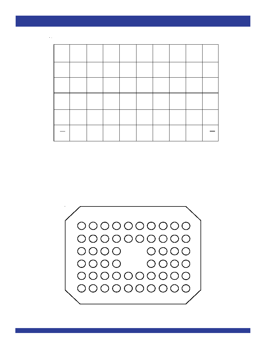
VFBGA
56 BALL VFBGA PACKAGE LAYOUT
PINOUT CONFIGURATION
1
2
3
4
5
6
A
B
C
D
E
F
G
H
J
K
A
1CLK
NC
NC
NC
NC
1OE
B
1D2
1D1
GND
GND
1Q1
1Q3
1Q7
2Q2
2Q4
2Q6
2Q8
1Q5
C
1D4
1D3
V
DD
V
DD
E
1D8
1D7
F
2D1
2D2
G
2D3
2D4
GND
GND
H
2D5
2D6
V
DD
V
DD
J
2D7
2D8
GND
GND
K
2CLK
2OE
NC
NC
NC
NC
D
1D6
1D5
GND
GND
6
5
4
3
2
1
1Q2
1Q4
1Q8
2Q1
2Q3
2Q5
2Q7
1Q6
NOTE:
NC = No Internal Connection
TOP VIEW
INDUSTRIAL TEMPERATURE RANGE
IDT74AUC16374
1.8V CMOS 16-BIT EDGE-TRIGGERED D-TYPE FLIP-FLOP
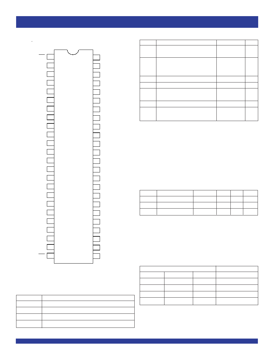
3
TSSOP/ TVSOP
TOP VIEW
PIN CONFIGURATION
Symbol
Description
Max
Unit
V
TERM
Terminal Voltage with Respect to GND
≠0.5 to +3.6
V
(all input and V
DD
terminals)
V
TERM
Terminal Voltage with Respect to GND
≠0.5 to +3.6
V
(any I/O or Output terminals in high-
impedance or power-off state)
T
STG
Storage Temperature
≠65 to +150
∞C
I
OUT
Continuous DC Output Current
±20
mA
I
IK
Continuous Clamp Current,
±50
mA
V
I
< 0, or V
I
> V
DD
I
OK
Continuous Clamp Current, V
O
< 0
≠50
mA
I
DD
Continuous Current through
±100
mA
I
SS
each V
DD
or GND
ABSOLUTE MAXIMUM RATINGS
(1)
(1)
(1)
(1)
(1)
NOTE:
1. Stresses greater than those listed under ABSOLUTE MAXIMUM RATINGS may cause
permanent damage to the device. This is a stress rating only and functional operation
of the device at these or any other conditions above those indicated in the operational
sections of this specification is not implied. Exposure to absolute maximum rating
conditions for extended periods may affect reliability.
Symbol
Parameter
Conditions
Typ.
Max.
Unit
C
IN
(1)
Input Capacitance
V
IN
= 0V
3
pF
C
OUT
(2)
Output Capacitance
V
OUT
= 0V
5
pF
C
I
(3)
Input Port Capacitance
V
IN
= 0V
3
pF
CAPACITANCE
(T
A
= +25∞C, F = 1.0MHz, V
DD
= 2.5V)
NOTES:
1. Applies to Control Inputs.
2. Applies to Data Outputs.
3. Applies to Data Inputs.
FUNCTION TABLE
(EACH FLIP-FLOP)
(1)
NOTES:
1. H = HIGH Voltage Level
L = LOW Voltage Level
X = Don't Care
Z = High-Impedance
= LOW-to-HIGH Transition
2. Level of Q before the indicated steady-state conditions were established.
Inputs
Output
xOE
xCLK
xDx
xQx
L
H
H
L
L
L
L
H or L
X
Q
(2)
H
X
X
Z
PIN DESCRIPTION
Pin Names
Description
xDx
Data Inputs
xCLK
Clock Inputs
xQx
3-State Outputs
xOE
3-State Output Enable Inputs (Active LOW)
1
OE
1
Q
1
1
Q
2
GND
1
Q
3
1
Q
4
V
DD
1
Q
5
1
Q
6
GND
1
Q
7
1
Q
8
2
Q
1
2
Q
2
2
Q
4
2
OE
GND
V
DD
2
Q
5
2
Q
6
GND
2
Q
7
2
3
4
5
6
7
8
9
10
11
12
13
14
15
16
17
18
19
20
21
22
23
24
39
38
37
36
35
34
33
32
31
30
29
28
27
26
25
40
41
42
43
44
45
46
47
48
1
1
CLK
1
D
1
1
D
2
GND
1
D
3
1
D
4
V
DD
1
D
5
1
D
6
1
D
7
1
D
8
2
D
1
GND
2
D
3
2
D
4
2
D
5
2
D
6
GND
2
D
7
2
D
8
2
CLK
2
Q
3
2
Q
8
V
DD
2
D
2
GND

INDUSTRIAL TEMPERATURE RANGE
4
IDT74AUC16374
1.8V CMOS 16-BIT EDGE-TRIGGERED D-TYPE FLIP-FLOP
Symbol
Parameter
Test Conditions
Min.
Max.
Unit
V
DD
Supply Voltage
0.8
2.7
V
V
DD
= 0.8V
V
DD
--
V
DD
= 1.1V to 1.3V
0.65 x V
DD
--
V
IH
Input HIGH Voltage Level
V
DD
= 1.4V to 1.6V
0.65 x V
DD
--
V
V
DD
= 1.65V to 1.95V
0.65 x V
DD
--
V
DD
= 2.3V to 2.7V
1.7
--
V
DD
= 0.8V
--
0
V
DD
= 1.1V to 1.3V
--
0.35 x V
DD
V
IL
Input LOW Voltage Level
V
DD
= 1.4V to 1.6V
--
0.35 x V
DD
V
V
DD
= 1.65V to 1.95V
--
0.35 x V
DD
V
DD
= 2.3V to 2.7V
--
0.7
V
I
Input Voltage
0
2.7
V
V
O
Output Voltage
Active State
0
V
DD
V
3-State
0
2.7
V
DD
= 0.8V
--
≠0.7
V
DD
= 1.1V
--
≠3
I
OH
HIGH Level Output Current
V
DD
= 1.4V
--
≠5
mA
V
DD
= 1.65V
--
≠8
V
DD
= 2.3V
--
≠9
V
DD
= 0.8V
--
0.7
V
DD
= 1.1V
--
3
I
OL
LOW Level Output Current
V
DD
= 1.4V
--
5
mA
V
DD
= 1.65V
--
8
V
DD
= 2.3V
--
9
t/v
Input Transition Rise or Fall Time
--
20
ns/V
T
A
Operating Free-Air Temperature
≠40
+85
∞C
RECOMMENDED OPERATING CHARACTERISTICS
(1)
NOTE:
1. All unused inputs of the device must be held at V
DD
or GND to ensure proper operation.
Symbol
Parameter
Test Conditions
Min.
Typ.
Max.
Unit
I
IH
Input HIGH or LOW Current
V
DD
= 2.7V, V
I
= V
DD
or GND
--
--
±5
µA
I
IL
All Inputs
I
OFF
Input/Output Power Off Leakage
V
DD
=
0V, V
IN or
V
O
2.7V
--
--
±10
µA
I
OZH
High Impedance Output Current
V
DD
= 2.7V
V
O
= V
DD
--
--
±10
µA
I
OZL
(3-State Output Pins)
V
O
= GND
--
--
±10
I
DDL
Quiescent Power Supply Current
V
DD
= 0.8V to 2.7V
--
--
20
µA
I
DDH
V
IN
= GND or V
DD
I
DDZ
DC ELECTRICAL CHARACTERISTICS OVER OPERATING RANGE
(1)
Following Conditions Apply Unless Otherwise Specified:
Operating Conditions: T
A
= ≠40∞C to +85∞C
NOTE:
1. All unused inputs of the device must be held at V
DD
or GND to ensure proper operation.
INDUSTRIAL TEMPERATURE RANGE
IDT74AUC16374
1.8V CMOS 16-BIT EDGE-TRIGGERED D-TYPE FLIP-FLOP
5
Symbol
Parameter
Test Conditions
(1)
Min.
Typ.
Max.
Unit
V
OH
Output HIGH Voltage
V
DD
= 0.8V - 2.7V
I
OH
= ≠100
µA
V
DD
- 0.1
--
--
V
DD
= 0.8V
I
OH
= ≠0.7mA
--
0.55
--
V
DD
= 1.1V
(2)
I
OH
= ≠3mA
0.8
--
--
V
V
DD
= 1.4V
(3)
I
OH
= ≠5mA
1
--
--
V
DD
= 1.65V
(4)
I
OH
= ≠8mA
1.2
--
--
V
DD
= 2.3V
(5)
I
OH
= ≠9mA
1.8
--
--
V
OL
Output LOW Voltage
V
DD
= 0.8V - 2.7V
I
OH
= 100
µA
--
--
0.2
V
DD
= 0.8V
I
OL
= 0.7mA
--
0.25
--
V
DD
= 1.1V
(2)
I
OL
= 3mA
--
--
0.3
V
V
DD
= 1.4V
(3)
I
OL
= 5mA
--
--
0.4
V
DD
= 1.65V
(4)
I
OL
= 8mA
--
--
0.45
V
DD
= 2.3V
(5)
I
OH
= 9mA
--
--
0.6
OUTPUT DRIVE CHARACTERISTICS
NOTES:
1. V
IL
and V
IH
must be within the min. or max. range shown in the DC ELECTRICAL CHARACTERISTICS table for the appropriate V
DD
range. T
A
= -40∞C to +85∞C.
2. Demonstrates operation for nominal V
DD
= 1.2V.
3. Demonstrates operation for nominal V
DD
= 1.5V.
4. Demonstrates operation for nominal V
DD
= 1.8V.
5. Demonstrates operation for nominal V
DD
= 2.5V.
OPERATING CHARACTERISTICS, T
A
= 25∞C
(1)
Symbol
Parameter
Test Conditions
V
DD
= 0.8V V
DD
= 1.2V V
DD
= 1.5V V
DD
= 1.8V V
DD
= 2.5V Unit
C
PD
Power Dissipation Capacitance
(2)
1 f
DATA
= 5MHz
24
24
24.1
26.2
31.2
pF
(each
Outputs Enabled,
1 f
CLK
= 10MHz
output)
1 Output Switching
1 f
OUT
= 5MHz
OE = GND, C
L
= 0pF
C
PD(Z)
Power Dissipation Capacitance
1 f
DATA
= 5MHz
7.5
7.5
8
9.4
13.2
pF
Outputs Disabled,
1 f
CLK
= 10MHz
1 Clock and 1 Data Switching
f
OUT
= not switching
OE = V
DD
, C
L
= 0pF
C
PD
Power Dissipation Capacitance
(3)
1 f
DATA
= 0MHz
13.8
13.8
14
14.7
17.5
pF
(each
Outputs Disabled,
1 f
CLK
= 10MHz
clock)
Clock Only Switching
f
OUT
= not switching
OE = V
DD
, C
L
= 0pF
NOTES:
1. Total device C
PD
for multiple (x) outputs switching and (n) clocks inputs switching = {x * C
PD
(each output)} + {n C
PD
(each clock)}.
2. C
PD
(each output). This is the C
PD
for each data bit where each input and output circuit is operating at 5MHz. The clock frequency is 10MHz and the numbers shown are
minus the I
DD
component.
3. C
PD
(each clock); this is the C
PD
for each clock circuit, operating at 10MHz.
INDUSTRIAL TEMPERATURE RANGE
6
IDT74AUC16374
1.8V CMOS 16-BIT EDGE-TRIGGERED D-TYPE FLIP-FLOP
SWITCHING CHARACTERISTICS
(1)
NOTE:
1. See TEST CIRCUITS AND WAVEFORMS. T
A
= -40∞C to +85∞C.
V
DD
= 0.8V V
DD
= 1.2V±0.1V
V
DD
= 1.5V±0.1V
V
DD
= 1.8V±0.15V
V
DD
= 2.5V±0.2V
Symbol
Parameter
Typ.
Min.
Max.
Min.
Max.
Min.
Typ.
Max.
Min.
Max.
Unit
f
MAX
85
--
250
--
250
--
--
250
--
250
MHz
t
PLH
Propagation Delay
7.3
1
4.5
0.8
2.9
0.7
1.5
2.8
0.7
2.2
ns
t
PHL
xCLK to xQx
t
PZH
Output Enable Time
7
1.2
5.3
0.8
3.6
0.8
1.5
2.9
0.7
2.2
ns
t
PZL
xOE to xQx
t
PHZ
Output Disable Time
8.2
2
7.1
1
4.8
1.4
2.7
4.5
0.7
2.2
ns
t
PLZ
xOE to xQx
f
CLOCK
Clock Frequency
85
250
--
250
--
250
--
--
250
--
MHz
t
SU
Set-up Time, Data before CLK
1.4
1
--
1
--
1
--
--
1
--
ns
t
H
Hold Time, Data after CLK
0.1
0.9
--
0.9
--
0.9
--
--
0.9
--
ns
t
W
Pulse Duration,
5.9
1.9
--
1.9
--
1.9
--
--
1.9
--
ns
CLK HIGH or LOW
INDUSTRIAL TEMPERATURE RANGE
IDT74AUC16374
1.8V CMOS 16-BIT EDGE-TRIGGERED D-TYPE FLIP-FLOP
7
Open
V
LOAD
GND
V
DD
Pulse
Generator
D.U.T.
R
L
C
L
R
T
V
IN
V
OUT
(1)
SAME PHASE
INPUT TRANSITION
OPPOSITE PHASE
INPUT TRANSITION
0V
0V
V
OH
V
OL
t
PLH
t
PHL
t
PHL
t
PLH
OUTPUT
V
DD
V
T
V
T
V
DD
V
T
CONTROL
INPUT
t
PLZ
0V
OUTPUT
NORMALLY
LOW
t
PZH
0V
SWITCH
CLOSED
OUTPUT
NORMALLY
HIGH
ENABLE
DISABLE
SWITCH
OPEN
t
PHZ
0V
V
OL +
V
LZ
V
OH
V
T
V
T
t
PZL
V
LOAD/2
V
LOAD/2
V
DD
V
T
V
OL
V
OH -
V
HZ
R
L
TIMING
INPUT
DATA
INPUT
t
SU
t
H
V
T
V
DD
0V
0V
V
DD
V
T
V
T
LOW-HIGH-LOW
PULSE
HIGH-LOW-HIGH
PULSE
0V
V
DD
V
T
V
T
t
W
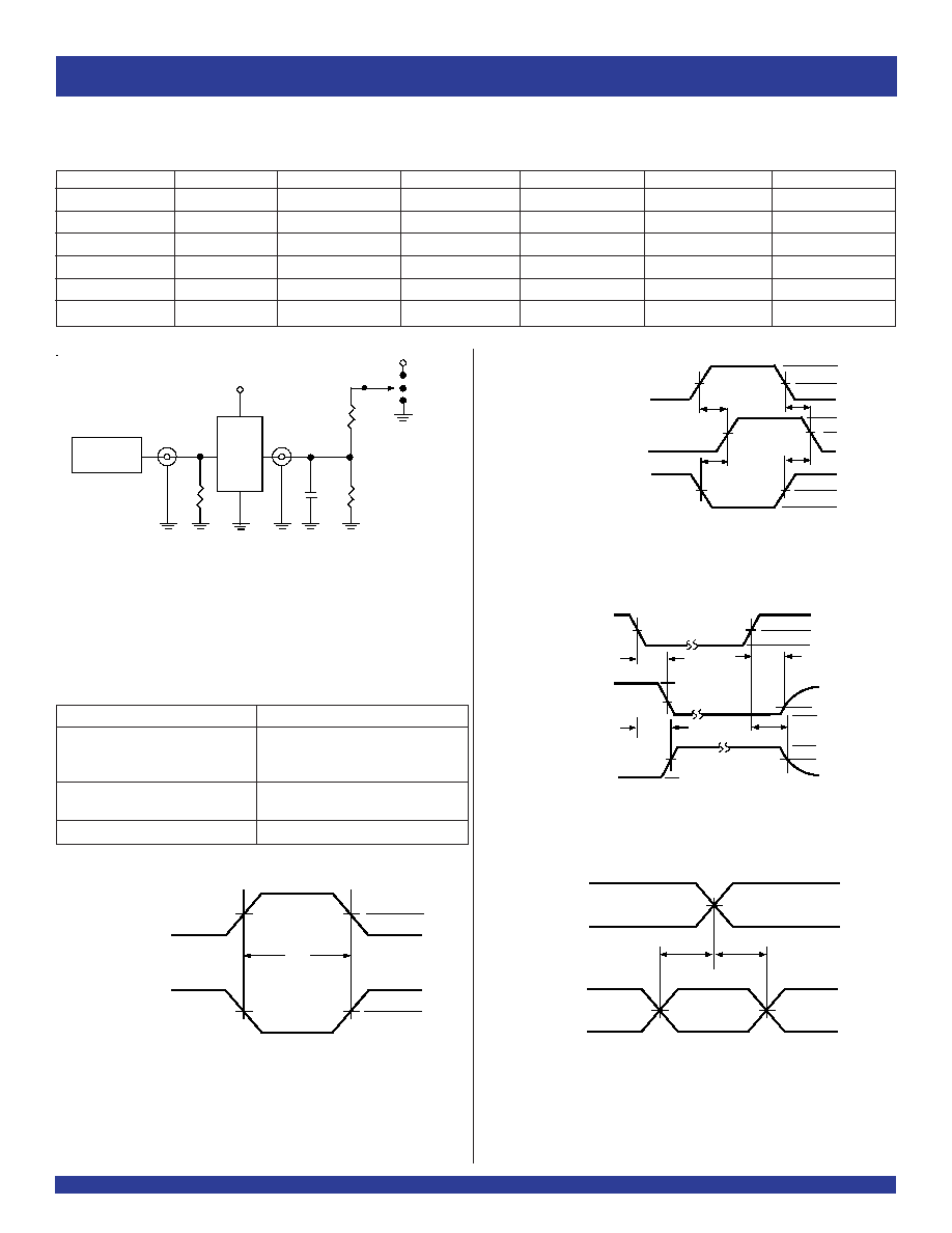
TEST CIRCUITS AND WAVEFORMS
Propagation Delay
Test Circuits for All Outputs
Enable and Disable Times
NOTE:
1. Diagram shown for input Control Enable-LOW and input Control Disable-HIGH.
DEFINITIONS:
C
L
= Load capacitance: includes jig and probe capacitance.
R
T
= Termination resistance: should be equal to Z
OUT
of the Pulse Generator.
NOTE:
1. Pulse Generator for All Pulses: Rate
10MHz; slew rate 1V/ns.
Test
Switch
Open Drain
Disable Low
V
LOAD
Enable Low
Disable High
GND
Enable High
All Other Tests
Open
SWITCH POSITION
Setup and Hold Times
TEST CONDITIONS
(1)
Symbol
V
DD
= 0.8V
V
DD
= 1.2V±0.1V
V
DD
= 1.5V±0.1V
V
DD
= 1.8V±0.15V
V
DD
= 2.5V±0.2V
Unit
V
LOAD
2xV
DD
2xV
DD
2xV
DD
2xV
DD
2xV
DD
V
V
T
V
DD
/2
V
DD
/2
V
DD
/2
V
DD
/2
V
DD
/2
V
V
LZ
100
100
100
150
150
mV
V
HZ
100
100
100
150
150
mV
R
L
2
2
2
1
0.5
K
C
L
15
15
15
30
30
pF
Pulse Width

INDUSTRIAL TEMPERATURE RANGE
8
IDT74AUC16374
1.8V CMOS 16-BIT EDGE-TRIGGERED D-TYPE FLIP-FLOP
ORDERING INFORMATION
CORPORATE HEADQUARTERS
for SALES:
for Tech Support:
2975 Stender Way
800-345-7015 or 408-727-6116
logichelp@idt.com
Santa Clara, CA 95054
fax: 408-492-8674
(408) 654-6459
www.idt.com
IDT
XX
AUC
XXX
XX
Package
Device Type
Temp. Range
BV
PA
PF
16
74
Very Fine Pitch Ball Grid Array
Thin Shrink Small Outline Package
Thin Very Small Outline Package
16-Bit Edge-Triggered D-Type Flip-
Flop with 3-State Outputs
≠ 40∞C to +85∞C
XX
Family
374
Double-Density
X
Bus- Hold
Blank
No bus-hold
X
Temp.
I
Industrial Temperature Range