 | –≠–ª–µ–∫—Ç—Ä–æ–Ω–Ω—ã–π –∫–æ–º–ø–æ–Ω–µ–Ω—Ç: 74FCT161T | –°–∫–∞—á–∞—Ç—å:  PDF PDF  ZIP ZIP |

INDUSTRIAL TEMPERATURE RANGE
IDT74FCT161AT/CT
FAST CMOS SYNCHRONOUS PRESETTABLE BINARY COUNTER
1
MARCH 2002
INDUSTRIAL TEMPERATURE RANGE
The IDT logo is a registered trademark of Integrated Device Technology, Inc.
© 2002 Integrated Device Technology, Inc.
DSC-5504/2
.EATURES:
∑ A and C grades
∑ Low input and output
1µA (max.)
∑ CMOS power levels
∑ True TTL input and output compatibility:
≠ V
OH
= 3.3V (typ.)
≠ V
OL
= 0.3V (typ.)
∑ High Drive outputs (-15mA I
OH
, 48mA I
OL
)
∑ Meets or exceeds JEDEC standard 18 specifications
∑ Power off disable outputs permit "live insertion"
∑ Available in SOIC and QSOP packages
.UNCTIONAL BLOCK DIAGRAM
IDT74FCT161AT/CT
FAST CMOS
SYNCHRONOUS
PRESETTABLE
BINARY COUNTER
DESCRIPTION:
The IDT74FCT161T is a high-speed synchronous modulo-16 binary
counter built using an advanced dual metal CMOS technology. It is
synchronously presettable for application in programmable dividers and
has two types of count enable inputs plus a terminal count output for versatility
in forming synchronous multi-stage counters. The IDT74FCT161T has
asynchronous Master Reset inputs that override all other inputs and force
the outputs low.
3
0
D CP
D
Q
Q
C
D
CP
DETAIL
A
DETAIL
A
DETAIL
A
PE
CEP
CET
CP
MR
Q
0
Q
1
Q
2
Q
3
Q
0
DETAIL A
P
0
P
1
P
2
P
3
TC
CP

INDUSTRIAL TEMPERATURE RANGE
2
IDT74FCT161AT/CT
FAST CMOS SYNCHRONOUS PRESETTABLE BINARY COUNTER
PIN CON.IGURATION
Symbol
Description
Max
Unit
V
TERM
(2)
Terminal Voltage with Respect to GND
≠0.5 to +7
V
V
TERM
(3)
Terminal Voltage with Respect to GND
≠0.5 to V
CC
+0.5
V
T
STG
Storage Temperature
≠65 to +150
∞ C
I
OUT
DC Output Current
≠60 to +120
mA
ABSOLUTE MAXIMUM RATINGS
(1)
NOTES:
1. Stresses greater than those listed under ABSOLUTE MAXIMUM RATINGS may cause
permanent damage to the device. This is a stress rating only and functional operation
of the device at these or any other conditions above those indicated in the operational
sections of this specification is not implied. Exposure to absolute maximum rating
conditions for extended periods may affect reliability. No terminal voltage may exceed
Vcc by +0.5V unless otherwise noted.
2. Inputs and Vcc terminals only.
3. Output and I/O terminals only.
Symbol
Parameter
(1)
Conditions
Typ.
Max.
Unit
C
IN
Input Capacitance
V
IN
= 0V
6
10
pF
C
OUT
Output Capacitance
V
OUT
= 0V
8
12
pF
CAPACITANCE
(T
A
= +25∞C, F = 1.0MHz)
NOTE:
1. This parameter is measured at characterization but not tested.
SOIC/ QSOP
TOP VIEW
2
3
4
5
6
7
8
9
10
11
12
13
14
15
16
1
MR
CP
GND
CEP
P
0
TC
Q
0
Q
1
Q
2
Q
3
CET
PE
V
CC
P
1
P
2
P
3
PIN DESCRIPTION
Pin Names
Description
CEP
Count Enable Parallel Input
CET
Count Enable Trickle Input
C P
Clock Pulse Input (Active Rising Edge)
MR
Asynchronous Master Reset Input (Active LOW)
P
0-3
Parallel Data Inputs
PE
Parallel Enable Input (Active LOW)
Q
0-3
Flip-Flop Outputs
TC
Terminal Count Output
.UNCTION TABLE
(1)
Action on the Rising
PE
CET
CEP
Clock Edge(s)
X
X
X
Reset (Clear)
L
X
X
Load (Px
Qx)
H
H
H
Count (Increment)
H
L
X
No Change (Hold)
H
X
L
No Change (Hold)
NOTE:
1. H = HIGH Voltage Level
L = LOW Voltage Level
X = Don't Care

INDUSTRIAL TEMPERATURE RANGE
IDT74FCT161AT/CT
FAST CMOS SYNCHRONOUS PRESETTABLE BINARY COUNTER
3
NOTES:
1. For conditions shown as Min. or Max., use appropriate value specified under Electrical Characteristics for the applicable device type.
2. Typical values are at V
CC
= 5.0V, +25∞C ambient.
3. Not more than one output should be tested at one time. Duration of the test should not exceed one second.
4. The test limit for this parameter is ±5µA at T
A
= ≠55∞C.
5. Clock pin requires a minimum V
IH
of 2.5V.
DC ELECTRICAL CHARACTERISTICS OVER OPERATING RANGE
Following Conditions Apply Unless Otherwise Specified:
Industrial: T
A
= ≠40∞C to +85∞C, V
CC
= 5.0V ± 5%
Symbol
Parameter
Test Conditions
(1)
Min.
Typ.
(2)
Max.
Unit
V
IH
Input HIGH Level
Guaranteed Logic HIGH Level
(5)
2V
--
--
V
V
IL
Input LOW Level
Guaranteed Logic LOW Level
--
--
0.8
V
I
IH
Input HIGH Current
(4)
V
CC
= Max.
V
I
= 2.7V
--
--
±1
µ A
I
IL
Input LOW Current
(4)
V
CC
= Max.
V
I
= 0.5V
--
--
±1
µ A
I
I
Input HIGH Current
(4)
V
CC
= Max., V
I
= V
CC
(Max.)
--
--
±1
µ A
V
IK
Clamp Diode Voltage
V
CC
= Min., I
N
= ≠18mA
--
≠0.7
≠1.2
V
I
OS
Short Circuit Current
V
CC
= Max.
(3)
, V
O
= GND
≠60
≠120
≠225
mA
V
OH
Output HIGH Voltage
V
CC
= Min.
I
OH
= ≠8mA
2.4
3.3
--
V
V
IN
= V
IH
or V
IL
I
OH
= ≠15mA
2
3
--
V
OL
Output LOW Voltage
V
CC
= Min.
I
OL
= 48mA
--
0.3
0.5
V
V
IN
= V
IH
or V
IL
V
H
Input Hysteresis
--
--
200
--
mV
I
CC
Quiescent Power
V
CC
= Max.
--
0.01
1
mA
Supply Current
V
IN
= GND or V
CC

INDUSTRIAL TEMPERATURE RANGE
4
IDT74FCT161AT/CT
FAST CMOS SYNCHRONOUS PRESETTABLE BINARY COUNTER
POWER SUPPLY CHARACTERISTICS
Symbol
Parameter
Test Conditions
(1)
Min.
Typ.
(2)
Max.
Unit
I
CC
Quiescent Power Supply Current
V
CC
= Max.
--
0.5
2
mA
TTL Inputs HIGH
V
IN
= 3.4V
(3)
I
CCD
Dynamic Power Supply Current
(4)
V
CC
= Max., Outputs Open
V
IN
= V
CC
--
0.15
0.25
mA/
Load Mode
V
IN
= GND
MHz
CEP = CET =
PE = GND
MR = V
CC
One Input Toggling
50% Duty Cycle
I
C
Total Power Supply Current
(6)
V
CC
= Max., Outputs Open
V
IN
= V
CC
--
1.5
3.5
mA
Load Mode
V
IN
= GND
f
CP
= 10MHz
50% Duty Cycle
CEP = CET =
PE = GND
V
IN
= 3.4V
--
2
5.5
MR = V
CC
V
IN
= GND
One Bit Toggling
at f
i
= 5MHz
50% Duty Cycle
V
CC
= Max., Outputs Open
V
IN
= V
CC
--
3.8
7.3
(5)
Load Mode
V
IN
= GND
f
CP
= 10MHz
50% Duty Cycle
CEP = CET =
PE = GND
V
IN
= 3.4V
--
5
12.3
(5)
MR = V
CC
V
IN
= GND
Four Bits Toggling
at f
i
= 5MHz
50% Duty Cycle
NOTES:
1. For conditions shown as Max. or Min., use appropriate value specified under Electrical Characteristics for the applicable device type.
2. Typical values are at V
CC
= 5.0V, +25∞C ambient.
3. Per TTL driven input (V
IN
= 3.4V). All other inputs at V
CC
or GND.
4. This parameter is not directly testable, but is derived for use in Total Power Supply Calculations.
5. Values for these conditions are examples of the I
CC
formula. These limits are guaranteed but not tested.
6. I
C
= I
QUIESCENT
+ I
INPUTS
+ I
DYNAMIC
I
C
= I
CC
+
I
CC
D
H
N
T
+ I
CCD
(f
CP/
2 + f
i
N
i
)
I
CC
= Quiescent Current
I
CC
= Power Supply Current for a TTL High Input (V
IN
= 3.4V)
D
H
= Duty Cycle for TTL Inputs High
N
T
= Number of TTL Inputs at D
H
I
CCD
= Dynamic Current Caused by an Input Transition Pair (HLH or LHL)
f
CP
= Clock Frequency for Register Devices (Zero for Non-Register Devices)
f
i
= Input Frequency
N
i
= Number of Inputs at f
i
All currents are in milliamps and all frequencies are in megahertz.

INDUSTRIAL TEMPERATURE RANGE
IDT74FCT161AT/CT
FAST CMOS SYNCHRONOUS PRESETTABLE BINARY COUNTER
5
SWITCHING CHARACTERISTICS OVER OPERATING RANGE
IDT74FCT161AT
IDT74FCT161CT
Symbol
Parameter
Condition
(1)
Min.
(2)
Max.
Min.
(2)
Max.
Unit
t
PLH
Propagation Delay
C
L
= 50pF
2
7.2
2
5.8
ns
t
PHL
CP to Qx (
PE Input HIGH)
R
L
= 500
t
PLH
Propagation Delay
2
6.2
2
5.8
ns
t
PHL
CP to Qx (
PE Input LOW)
t
PLH
Propagation Delay
2
9.8
2
7.4
ns
t
PHL
CP to TC
t
PLH
Propagation Delay
1.5
5.5
1.5
5.2
ns
t
PHL
CET to TC
t
PHL
Propagation Delay
2
8.5
2
6
ns
MR to Qx
t
PHL
Propagation Delay
2
7.5
2
7
ns
MR to TC
t
SU
Set-up Time, HIGH or LOW, Px to CP
4
--
4
--
ns
t
H
Hold Time, HIGH or LOW, Px to CP
1.5
--
1.5
--
ns
t
SU
Set-up Time, HIGH or LOW,
PE or SR to CP
9.5
--
9.5
--
ns
t
H
Hold Time, HIGH or LOW,
PE or SR to CP
1.5
--
1.5
--
ns
t
SU
Set-up Time, HIGH or LOW, CEP or CET to CP
9.5
--
9.5
--
ns
t
H
Hold Time, HIGH or LOW, CEP or CET to CP
0
--
0
--
ns
t
W
Clock Pulse, Width (Load) HIGH or LOW
4
(3)
--
4
(3)
--
ns
t
W
Clock Pulse, Width (Count) HIGH or LOW
6
--
6
--
ns
t
PHL
MR Pulse Width LOW
4
(3)
--
4
(3)
--
ns
t
PHL
Recovery Time
MR to CP
5
--
5
--
ns
NOTES:
1. See test circuits and waveforms.
2. Minimum limits are guaranteed but not tested on Propagation Delays.
3. This limit is guaranteed but not tested.
INDUSTRIAL TEMPERATURE RANGE
6
IDT74FCT161AT/CT
FAST CMOS SYNCHRONOUS PRESETTABLE BINARY COUNTER
Pulse
Generator
R
T
D.U.T
.
V
CC
V
IN
C
L
V
OUT
50pF
500
500
7.0V
3V
1.5V
0V
3V
1.5V
0V
3V
1.5V
0V
3V
1.5V
0V
DATA
INPUT
TIMING
INPUT
ASYNCHRONOUS CONTROL
PRESET
CLEAR
ETC.
SYNCHRONOUS CONTROL
t
SU
t
H
t
REM
t
SU
t
H
HIGH-LOW-HIGH
PULSE
LOW-HIGH-LOW
PULSE
t
W
1.5V
1.5V
SAME PHASE
INPUT TRANSITION
3V
1.5V
0V
1.5V
V
OH
t
PLH
OUTPUT
OPPOSITE PHASE
INPUT TRANSITION
3V
1.5V
0V
t
PLH
t
PHL
t
PHL
V
OL
CONTROL
INPUT
3V
1.5V
0V
3.5V
0V
OUTPUT
NORMALLY
LOW
OUTPUT
NORMALLY
HIGH
SWITCH
CLOSED
SWITCH
OPEN
V
OL
0.3V
0.3V
t
PLZ
t
PZL
t
PZH
t
PHZ
3.5V
0V
1.5V
1.5V
ENABLE
DISABLE
V
OH
PRESET
CLEAR
CLOCK ENABLE
ETC.
Octal link
Octal link
Octal link
Octal link
Octal link
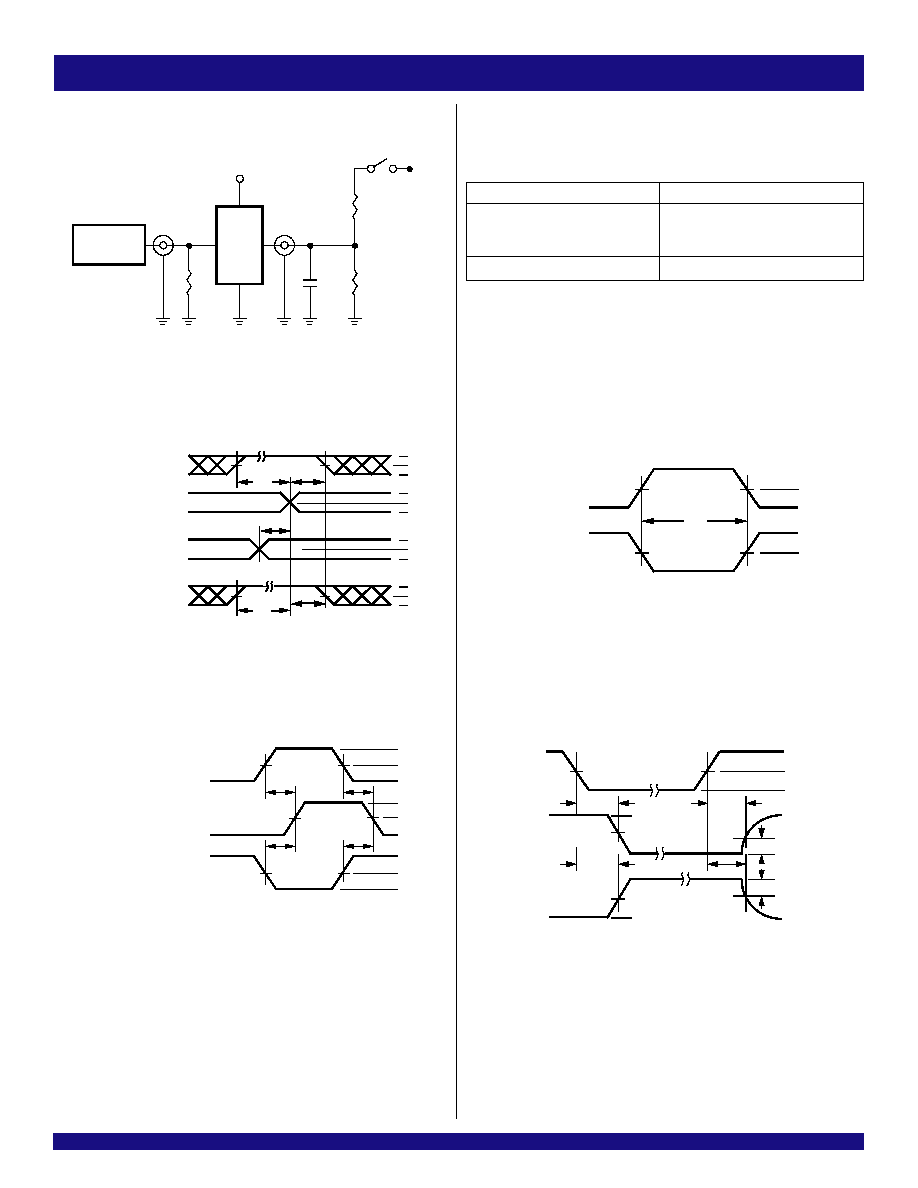
TEST CIRCUITS AND WAVE.ORMS
Propagation Delay
Test Circuits for All Outputs
Enable and Disable Times
Set-Up, Hold, and Release Times
Pulse Width
NOTES:
1. Diagram shown for input Control Enable-LOW and input Control Disable-HIGH.
2. Pulse Generator for All Pulses: Rate
1.0MHz; t
F
2.5ns; t
R
2.5ns.
Test
Switch
Open Drain
Disable Low
Closed
Enable Low
All Other Tests
Open
SWITCH POSITION
DEFINITIONS:
C
L
= Load capacitance: includes jig and probe capacitance.
R
T
= Termination resistance: should be equal to Z
OUT
of the Pulse Generator.

INDUSTRIAL TEMPERATURE RANGE
IDT74FCT161AT/CT
FAST CMOS SYNCHRONOUS PRESETTABLE BINARY COUNTER
7
ORDERING IN.ORMATION
Synchronous Presettable Binary Counter
X
Temperature
Range
XXXX
Device
Type
X
Package
FCT
IDT
SO
Q
Small Outline IC
Quarter-size Small Outline Package
- 40∞ to +85∞C
74
161AT
161CT
CORPORATE HEADQUARTERS
for SALES:
for Tech Support:
2975 Stender Way
800-345-7015 or 408-727-6116
logichelp@idt.com
Santa Clara, CA 95054
fax: 408-492-8674
(408) 654-6459
www.idt.com
3/25/2002
Removed standard speed grade
DATA SHEET DOCUMENT HISTORY