1
IDT74FCT16652AT/CT
FAST CMOS 16-BIT BUS TRANSCEIVER/REGISTER
INDUSTRIAL TEMPERATURE RANGE
JUNE 2002
IDT74FCT16652AT/CT
INDUSTRIAL TEMPERATURE RANGE
FAST CMOS 16-BIT BUS
TRANSCEIVER/REGISTER
DESCRIPTION:
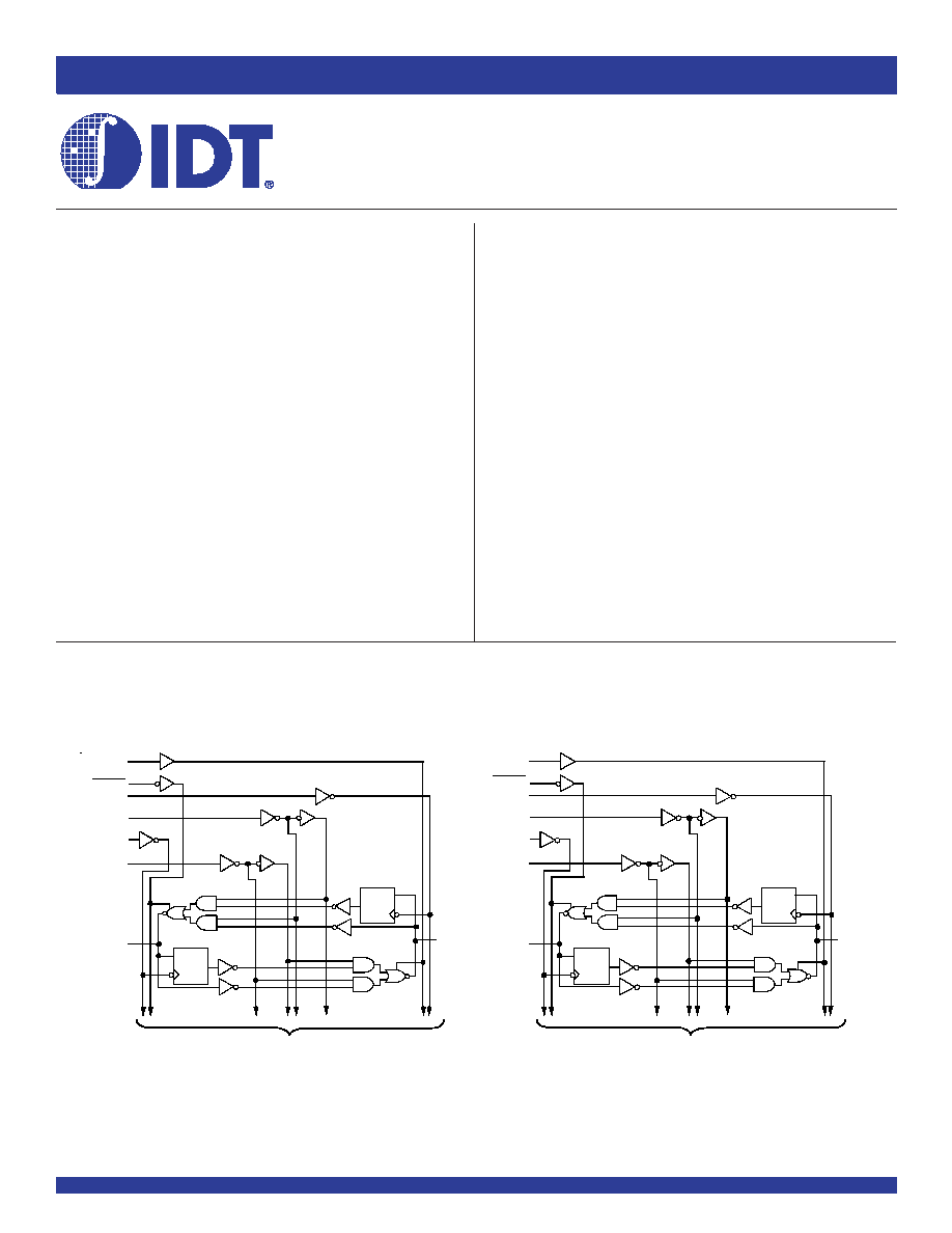
The FCT16652T 16-bit registered transceivers are built using advanced
dual metal CMOS technology. These high-speed, low-power devices are
organized as two independent 8-bit bus transceivers with 3-state D-type
registers. For example, the xOEAB and xOEBA signals control the transceiver
functions.
The xSAB and xSBA control pins are provided to select either real time or
stored data transfer. The circuitry used for select control will eliminate the typical
decoding glitch that occurs in a multiplexer during the transition between stored
and real time data. A low input level selects real-time data and a high level selects
stored data.
Data on the A or B data bus, or both, can be stored in the internal D-flip-flops
by low-to-high transitions at the appropriate clock pins (xCLKAB or xCLKBA),
regardless of the select or enable control pins. Flow-through organization of
signal pins simplifies layout. All inputs are designed with hysteresis for improved
noise margin.
The FCT16652T is ideally suited for driving high capacitance loads and low-
impedance backplanes. The output buffers are designed with power off disable
capability to allow "live insertion" of boards when used as backplane drivers.
1
A
1
1
O EBA
1
CLKBA
1
SBA
1
CLKAB
1
SAB
1
OE AB
1
B
1
B R EG
A R EG
D
C
C
D
TO S E VE N O THE R CHA NNELS
2
B
1
2
CLK AB
2
O EBA
2
CLK BA
2
SBA
2
A
1
2
O EAB
2
SAB
TO S E VE N O THE R CHA NNE LS
B R EG
A R EG
D
C
C
D
FEATURES:
∑ 0.5 MICRON CMOS Technology
∑ High-speed, low-power CMOS replacement for ABT functions
∑ Typical t
SK(o)
(Output Skew) < 250ps
∑ Low input and output leakage
1µA (max.)
∑ V
CC
= 5V ±10%
∑ High drive outputs (≠32mA I
OH
, 64mA I
OL
)
∑ Power off disable outputs permit "live insertion"
∑ Typical V
OLP
(Output Ground Bounce) < 1.0V at V
CC
= 5V,
T
A
= 25∞C
∑ Available in SSOP and TSSOP packages
FUNCTIONAL BLOCK DIAGRAM
The IDT logo is a registered trademark of Integrated Device Technology, Inc.
© 2002 Integrated Device Technology, Inc.
DSC-5450/2
2
INDUSTRIAL TEMPERATURE RANGE
IDT74FCT16652AT/CT
FAST CMOS 16-BIT BUS TRANSCEIVER/REGISTER
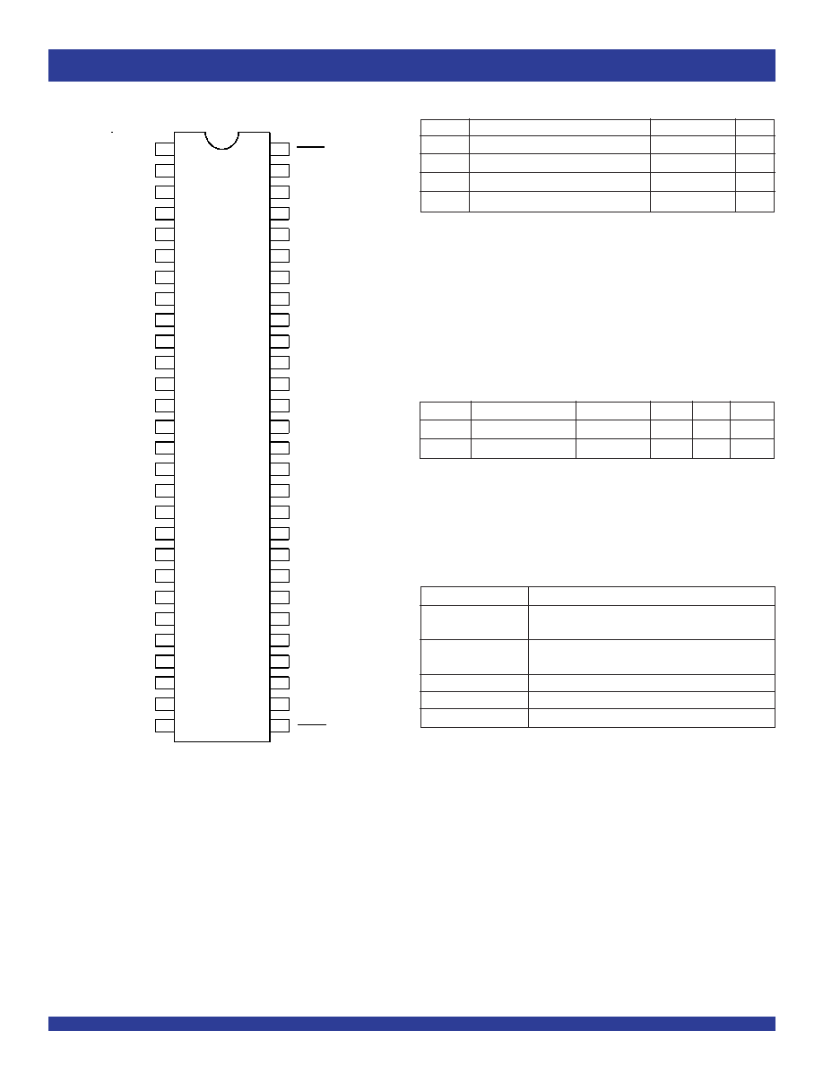
SSOP/ TSSOP
TOP VIEW
PIN CONFIGURATION
1
B
1
1
B
2
G ND
1
B
3
1
B
4
V
C C
1
B
5
1
B
6
1
OE BA
1
SBA
1
B
7
1
B
8
2
B
1
2
B
2
G ND
2
B
3
2
B
4
V
C C
2
B
5
G ND
1
CLKBA
2
B
7
2
B
6
2
B
8
G ND
2
SBA
2
CLKBA
2
OE BA
1
OE AB
1
CLKAB
1
SAB
G ND
1
A
1
1
A
2
V
C C
1
A
3
1
A
4
G ND
1
A
5
1
A
6
1
A
7
1
A
8
G ND
2
A
1
2
A
2
V
C C
2
A
3
2
SAB
2
A
5
2
A
4
2
A
7
G ND
2
A
8
2
CLKAB
2O EAB
2
A
6
47
37
38
39
40
41
42
43
44
45
46
33
34
35
36
56
55
49
50
51
52
53
54
48
1
2
3
4
5
6
7
8
9
10
12
13
14
15
16
17
18
19
20
11
21
22
23
24
29
30
31
32
25
26
27
28
Symbol
Description
Max
Unit
V
TERM
(2)
Terminal Voltage with Respect to GND
≠0.5 to +7
V
V
TERM
(3)
Terminal Voltage with Respect to GND
≠0.5 to V
CC
+0.5
V
T
STG
Storage Temperature
≠65 to +150
∞C
I
OUT
DC Output Current
≠60 to +120
mA
ABSOLUTE MAXIMUM RATINGS
(1)
NOTES:
1. Stresses greater than those listed under ABSOLUTE MAXIMUM RATINGS may
cause permanent damage to the device. This is a stress rating only and functional
operation of the device at these or any other conditions above those indicated in
the operational sections of this specification is not implied. Exposure to absolute
maximum rating conditions for extended periods may affect reliability.
2. All device terminals except FCT162XXX Output and I/O terminals.
3. Output and I/O terminals for FCT162XXX.
Symbol
Parameter
(1)
Conditions
Typ.
Max.
Unit
C
IN
Input Capacitance
V
IN
= 0V
4.5
6
pF
C
OUT
Output Capacitance
V
OUT
= 0V
5.5
8
pF
CAPACITANCE
(T
A
= +25∞C, f = 1.0MHz)
NOTE:
1. This parameter is measured at characterization but not tested.
Pin Names
Description
xAx
Data Register A Inputs
Data Register B Outputs
xBx
Data Register B Inputs
Data Register A Outputs
xCLKAB, xCLKBA
Clock Pulse Inputs
xSAB, xSBA
Output Data Source Select Inputs
xOEAB xOEBA
Output Enable Inputs
PIN DESCRIPTION
3
IDT74FCT16652AT/CT
FAST CMOS 16-BIT BUS TRANSCEIVER/REGISTER
INDUSTRIAL TEMPERATURE RANGE
Inputs
Data I/O
(1)
xOEAB
xOEBA
xCLKAB
xCLKBA
xSAB
xSBA
xAx
xBx
Operation or Function
L
H
H or L
H or L
X
X
Input
Input
Isolation
L
H
X
X
Store A and B Data
X
H
H or L
X
X
Input
Unspecified
(1)
Store A, Hold B
H
H
X
(2)
X
Input
Output
Store A in Both Registers
L
X
H or L
X
X
Unspecified
(1)
Input
Hold A, Store B
L
L
X
X
(2)
Output
Input
Store B in Both Registers
L
L
X
X
X
L
Output
Input
Real Time B Data to A Bus
L
L
X
H or L
X
H
Stored B Data to A Bus
H
H
X
X
L
X
Input
Output
Real Time A Data to B Bus
H
H
H or L
X
H
X
Stored A Data to B Bus
H
L
H or L
H or L
H
H
Output
Output
Stored A Data to B Bus and
Stored B Data to A Bus
FUNCTION TABLE
NOTES:
1. The data output functions may be enabled or disabled by various signals at the xOEAB or xOEBA inputs. Data input functions are always enabled, i.e. data at the bus pins
will be stored on every LOW-to-HIGH transition on the clocks inputs.
2. Select control = L: clocks can occur simultaneously.
Select control = H: clocks must be staggered to load both registers.
3. H = HIGH Voltage Level
L = LOW Voltage Level
X = Don't care
= LOW-to-HIGH Transition
4
INDUSTRIAL TEMPERATURE RANGE
IDT74FCT16652AT/CT
FAST CMOS 16-BIT BUS TRANSCEIVER/REGISTER
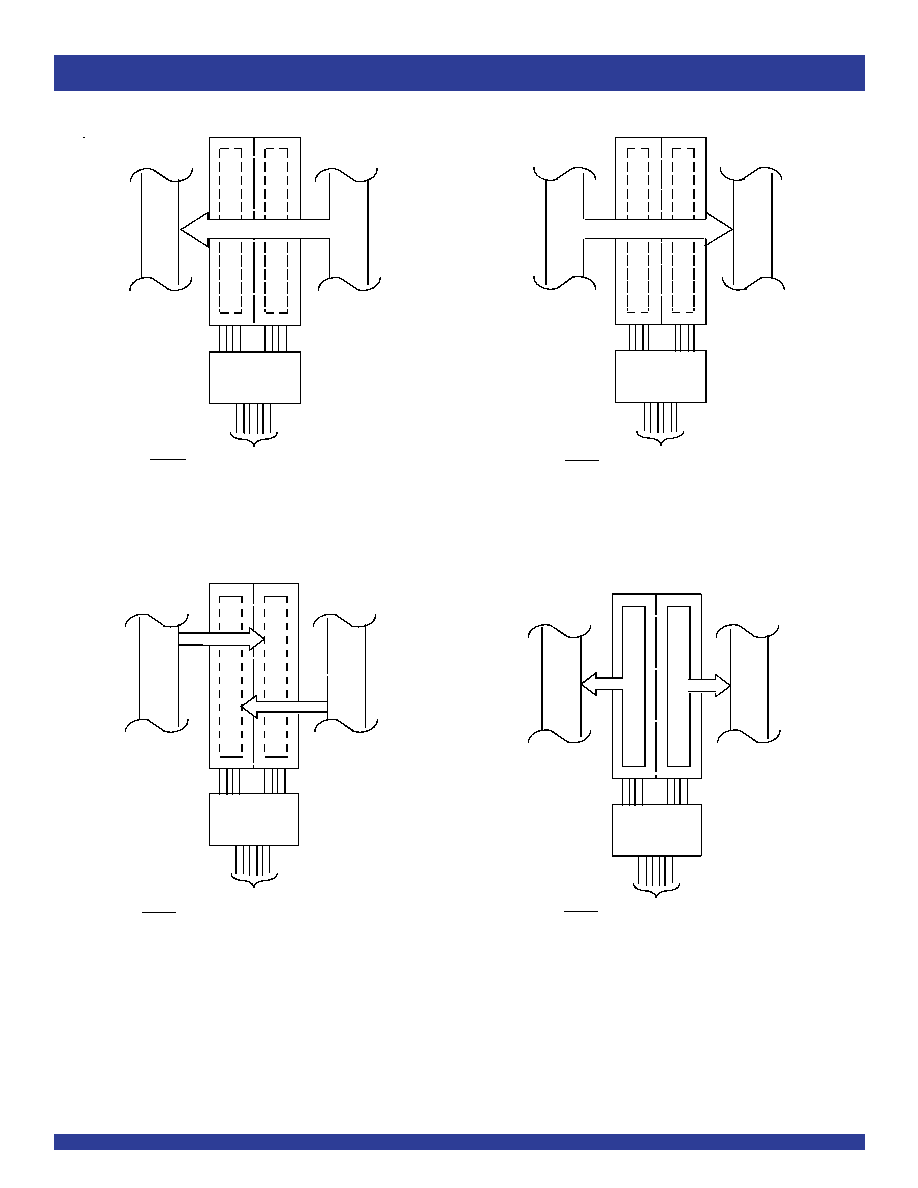
BUS
A
BU S
B
x
OEA B
x
O EBA
x
CLKAB
x
C LKBA
x
SAB
x
SBA
L
L
X
X
X
L
BU S
A
BUS
B
x
OEAB
x
OEBA
x
CLKAB
x
CLKB A
x
SAB
x
SBA
H
H
X
X
L
X
BUS
A
BU S
B
x
OEAB
x
OEBA
x
CLKA B
x
C LKBA
x
SAB
x
SBA
L
X
X
X
L
H
X
X
X
X
H
X
X
X
BUS
A
BUS
B
x
OEAB
x
OEBA
x
CLKAB
x
C LKBA
x
SAB
x
SBA
H
L
H or L
H
H or L
H
Real-Time Transfer
Bus B to A
Real-Time Transfer
Bus A to B
Storage from
A and/or B
Transfer Stored
Data to A and/or B
5
IDT74FCT16652AT/CT
FAST CMOS 16-BIT BUS TRANSCEIVER/REGISTER
INDUSTRIAL TEMPERATURE RANGE
Symbol
Parameter
Test Conditions
(1)
Min.
Typ.
(2)
Max.
Unit
V
IH
Input HIGH Level
Guaranteed Logic HIGH Level
2
--
--
V
V
IL
Input LOW Level
Guaranteed Logic LOW Level
--
--
0.8
V
I
IH
Input HIGH Current (Input pins)
(5)
V
CC
= Max.
V
I
= V
CC
--
--
±1
µA
Input HIGH Current (I/O pins)
(5)
--
--
±1
I
IL
Input LOW Current (Input pins)
(5)
V
I
= GND
--
--
±1
Input LOW Current (I/O pins)
(5)
--
--
±1
I
OZH
High Impedance Output Current
V
CC
= Max.
V
O
= 2.7V
--
--
±1
µA
I
OZL
(3-State Output pins)
(5)
V
O
= 0.5V
--
--
±1
V
IK
Clamp Diode Voltage
V
CC
= Min., I
IN
= ≠18mA
--
≠0.7
≠1.2
V
I
OS
Short Circuit Current
V
CC
= Max., V
O
= GND
(3)
≠80
≠140
≠250
mA
V
H
Input Hysteresis
--
--
100
--
mV
I
CCL
Quiescent Power Supply Current
V
CC
= Max
--
5
500
µA
I
CCH
V
IN
= GND or V
CC
I
CCZ
DC ELECTRICAL CHARACTERISTICS OVER OPERATING RANGE
Following Conditions Apply Unless Otherwise Specified:
Industrial: T
A
= ≠40∞C to +85∞C, V
CC
= 5.0V ±10%
NOTES:
1. For conditions shown as Min. or Max., use appropriate value specified under Electrical Characteristics for the applicable device type.
2. Typical values are at V
CC
= 5.0V, +25∞C ambient.
3. Not more than one output should be shorted at one time. Duration of the test should not exceed one second.
4. Duration of the condition can not exceed one second.
5. This test limit for this parameter is ±5µA at T
A
= ≠55∞C.
Symbol
Parameter
Test Conditions
(1)
Min.
Typ.
(2)
Max.
Unit
I
O
Output Drive Current
V
CC
= Max.
,
V
O
= 2.5V
(3)
≠50
--
≠180
mA
V
OH
Output HIGH Voltage
V
CC
= Min.
I
OH
= ≠3mA
2.5
3.5
--
V
IN
= V
IH
or V
IL
I
OH
= ≠15mA
2.4
3.5
--
V
I
OH
= ≠32mA
(4)
2
3
--
V
OL
Output LOW Voltage
V
CC
= Min.
I
OL
= 64mA
--
0.2
0.55
V
V
IN
= V
IH
or V
IL
I
OFF
Input/Output Power Off Leakage
(5)
V
CC
= 0V, V
IN
or V
O
4.5V
--
--
±1
µA
OUTPUT DRIVE CHARACTERISTICS
6
INDUSTRIAL TEMPERATURE RANGE
IDT74FCT16652AT/CT
FAST CMOS 16-BIT BUS TRANSCEIVER/REGISTER
Symbol
Parameter
Test Conditions
(1)
Min.
Typ.
(2)
Max.
Unit
I
CC
Quiescent Power Supply Current
V
CC
= Max.
--
0.5
1.5
mA
TTL Inputs HIGH
V
IN
= 3.4V
(3)
I
CCD
Dynamic Power Supply Current
(4)
V
CC
= Max.
V
IN
= V
CC
--
75
120
µA/
Outputs Open
V
IN
= GND
MHz
xOEAB = xOEBA = GND
One Input Toggling
50% Duty Cycle
I
C
Total Power Supply Current
(6)
V
CC
= Max.
V
IN
= V
CC
--
0.8
1.7
mA
Outputs Open
V
IN
= GND
f
CP
= 10MHz (xCLKBA)
50% Duty Cycle
xOEAB = xOEBA = GND
V
IN
= 3.4V
--
1.3
3.2
One Bit Toggling
V
IN
= GND
fi = 5MHz
50% Duty Cycle
V
CC
= Max.
V
IN
= V
CC
--
3.8
6.5
(5)
Outputs Open
V
IN
= GND
f
CP
= 10MHz (xCLKBA)
50% Duty Cycle
xOEAB = xOEBA = GND
V
IN
= 3.4V
--
8.3
20
(5)
Sixteen Bits Toggling
V
IN
= GND
fi = 2.5MHz
50% Duty Cycle
NOTES:
1. For conditions shown as Min. or Max., use appropriate value specified under Electrical Characteristics for the applicable device type.
2. Typical values are at V
CC
= 5.0V, +25∞C ambient.
3. Per TTL driven input (V
IN
= 3.4V). All other inputs at V
CC
or GND.
4. This parameter is not directly testable, but is derived for use in Total Power Supply Calculations.
5. Values for these conditions are examples of the I
CC
formula. These limits are guaranteed but not tested.
6. I
C
= I
QUIESCENT
+ I
INPUTS
+ I
DYNAMIC
I
C
= I
CC
+
I
CC
D
H
N
T
+ I
CCD
(f
CP
N
CP
/2 + fiNi)
I
CC
= Quiescent Current (I
CCL
, I
CCH
and I
CCZ
)
I
CC
= Power Supply Current for a TTL High Input (V
IN
= 3.4V)
D
H
= Duty Cycle for TTL Inputs High
N
T
= Number of TTL Inputs at D
H
I
CCD
= Dynamic Current Caused by an Input Transition Pair (HLH or LHL)
f
CP
= Clock Frequency for Register Devices (Zero for Non-Register Devices)
N
CP
= Number of Clock Inputs at f
CP
f
i
= Input Frequency
N
i
= Number of Inputs at f
i
POWER SUPPLY CHARACTERISTICS
7
IDT74FCT16652AT/CT
FAST CMOS 16-BIT BUS TRANSCEIVER/REGISTER
INDUSTRIAL TEMPERATURE RANGE
74FCT16652AT
74FCT16652CT
Symbol
Parameter
Condition
(1)
Min.
(2)
Max.
Min.
(2)
Max.
Unit
t
PLH
Propagation Delay
C
L
= 50pF
2
6.3
1.5
3.9
ns
t
PHL
Bus to Bus
R
L
= 500
t
PZH
Output Enable Time
2
9.8
1.5
4.8
ns
t
PZL
xOEAB or xOEBA to Bus
t
PHZ
Output Disable Time
2
6.3
1.5
4.4
ns
t
PLZ
xOEAB or xOEBA to Bus
t
PLH
Propagation Delay
2
6.3
1.5
4.1
ns
t
PHL
Clock to Bus
t
PLH
Propagation Delay
2
7.7
1.5
4.2
ns
t
PHL
xSBA or xSAB to Bus
t
SU
Set-Up Time, HIGH or LOW
2
--
2
--
ns
Bus to Clock
t
H
Hold Time, HIGH or LOW
1.5
--
0
--
ns
Bus to Clock
t
W
Clock Pulse Width, HIGH or LOW
5
--
3
--
ns
t
SK(o)
Output Skew
(3)
--
0.5
--
0.5
ns
SWITCHING CHARACTERISTICS OVER OPERATING RANGE
NOTES:
1. See test circuit and waveforms.
2. Minimum limits are guaranteed but not tested on Propagation Delays.
3. Skew between any two outputs of the same package switching in the same direction. This parameter is guaranteed by design.
8
INDUSTRIAL TEMPERATURE RANGE
IDT74FCT16652AT/CT
FAST CMOS 16-BIT BUS TRANSCEIVER/REGISTER
Pulse
Generator
R
T
D.U.T.
V
CC
V
IN
C
L
V
OUT
50pF
500
500
7.0V
3V
1.5V
0V
3V
1.5V
0V
3V
1.5V
0V
3V
1.5V
0V
DATA
INPUT
TIMING
INPUT
ASYNCHRONOUS CONTROL
PRESET
CLEAR
ETC.
SYNCHRONOUS CONTROL
t
SU
t
H
t
REM
t
SU
t
H
PRESET
CLEAR
CLOCK ENABLE
ETC.
HIGH-LOW-HIGH
PULSE
LOW-HIGH-LOW
PULSE
t
W
1.5V
1.5V
SAME PHASE
INPUT TRANSITION
3V
1.5V
0V
1.5V
V
OH
t
PLH
OUTPUT
OPPOSITE PHASE
INPUT TRANSITION
3V
1.5V
0V
t
PLH
t
PHL
t
PHL
V
OL
CONTROL
INPUT
3V
1.5V
0V
3.5V
0V
OUTPUT
NORMALLY
LOW
OUTPUT
NORMALLY
HIGH
SWITCH
CLOSED
SWITCH
OPEN
V
OL
0.3V
0.3V
t
PLZ
t
PZL
t
PZH
t
PHZ
3.5V
0V
1.5V
1.5V
ENABLE
DISABLE
V
OH
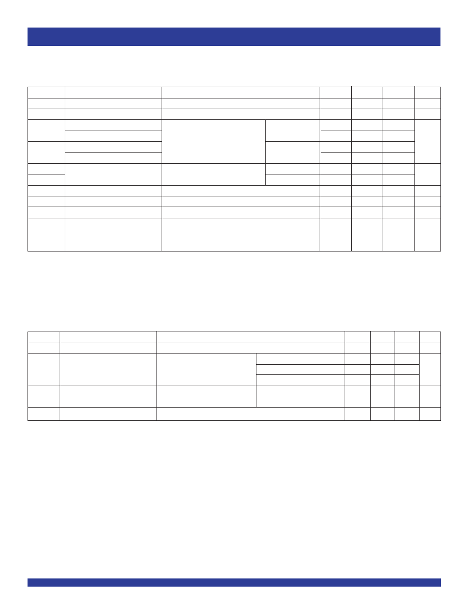
TEST CIRCUITS AND WAVEFORMS
Propagation Delay
Test Circuits for All Outputs
Enable and Disable Times
Set-up, Hold, and Release Times
Pulse Width
NOTES:
1. Diagram shown for input Control Enable-LOW and input Control Disable-HIGH.
2. Pulse Generator for All Pulses: Rate
1.0MHz; t
F
2.5ns; t
R
2.5ns.
Test
Switch
Open Drain
Disable Low
Closed
Enable Low
All Other Tests
Open
SWITCH POSITION
DEFINITIONS:
C
L
= Load capacitance: includes jig and probe capacitance.
R
T
= Termination resistance: should be equal to Z
OUT
of the Pulse Generator.
9
IDT74FCT16652AT/CT
FAST CMOS 16-BIT BUS TRANSCEIVER/REGISTER
INDUSTRIAL TEMPERATURE RANGE
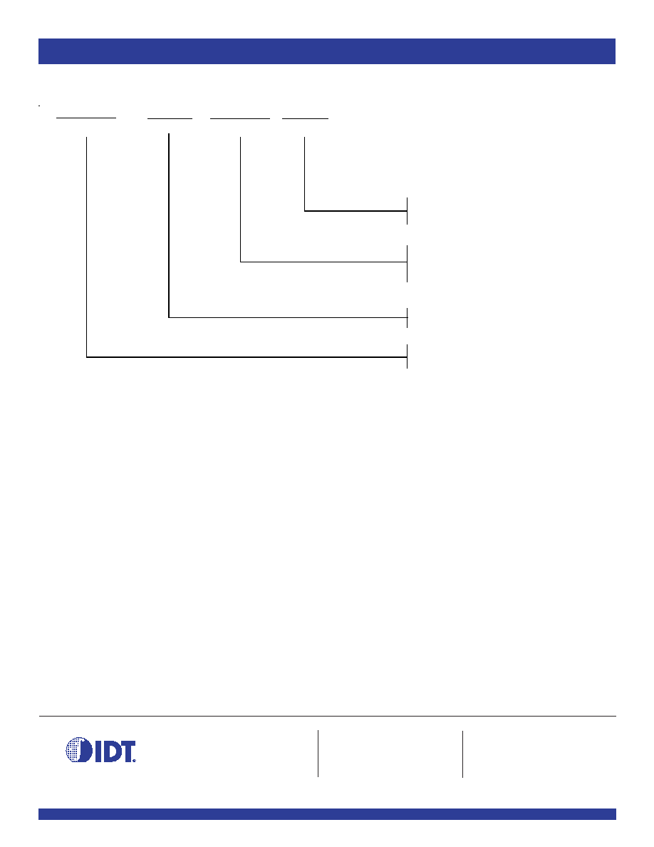
ORDERING INFORMATION
IDT XX
Temp. Range
XXXX
Device Type
XX
Package
PV
PA
Shrink Small Outline Package
Thin Shrink Small Outline Package
16-Bit Bus Transceiver/Register
74
≠ 40∞C to +85∞C
16
Double-Density, 5 Volt, High Drive
FCT
XXX
Family
652AT
652CT
DATA SHEET DOCUMENT HISTORY
1/21/2002
Removed Military temp grade
6/21/2002
Updated as per PDNs Logic-00-07 and Logic-01-04
CORPORATE HEADQUARTERS
for SALES:
for Tech Support:
2975 Stender Way
800-345-7015 or 408-727-6116
logichelp@idt.com
Santa Clara, CA 95054
fax: 408-492-8674
(408) 654-6459
www.idt.com