
INDUSTRIAL TEMPERATURE RANGE
IDT74FCT2652AT/CT
FAST CMOS OCTAL TRANSCEIVER/REGISTER (3-STATE)
1
AUGUST 2000
INDUSTRIAL TEMPERATURE RANGE
The IDT logo is a registered trademark of Integrated Device Technology, Inc.
© 2000 Integrated Device Technology, Inc.
DSC-5509/1
FEATURES:
∑ A and C grades
∑ Low input and output leakage
1µA (max.)
∑ CMOS power levels
∑ True TTL input and output compatibility:
≠ V
OH
= 3.3V (typ.)
≠ V
OL
= 0.3V (typ.)
∑ Resistor outputs (-15mA I
OH
, 12mA I
OL
)
∑ Meets or exceeds JEDEC standard 18 specifications
∑ Reduced system switching noise
∑ Power off disable outputs permit "live insertion"
∑ Available in SOIC and QSOP packages
FUNCTIONAL BLOCK DIAGRAM
IDT74FCT2652AT/CT
FAST CMOS OCTAL
TRANSCEIVER/
REGISTERS (3-STATE)
DESCRIPTION:
The FCT2652T consists of a bus transceiver with 3-state D-type flip-flops
and control circuitry arranged for multiplexed transmission of data directly
from the data bus or from the internal storage registers. The FCT2652T
utilizes GAB and GBA signals to control the transceiver functions.
SAB and SBA control pins are provided to select either real- time or stored
data transfer. The circuitry used for select control will eliminate the typical
decoding glitch that occurs in a multiplexer during the transition between
stored and real-time data. A low input level selects real-time data and a high
selects stored data.
Data on the A or B data bus, or both, can be stored in the internal D flip-
flops by low-to-high transitions at the appropriate clock pins (CPAB or
CPBA), regardless of the select or enable control pins.
The FCT2652T have balanced drive outputs with current limiting
resistors. This offers low ground bounce, minimal undershoot and con-
trolled output fall times-reducing the need for external series terminating
resistors. FCT2652T parts are plug-in replacements for FCT652T parts.
A1
CPB A
SBA
CPA B
SAB
GBA
G AB
O NE OF EIG HT CHANNELS
B REG
A REG
B1
1D
C1
C1
1D
TO SEVE N O THE R CHANNELS

INDUSTRIAL TEMPERATURE RANGE
2
IDT74FCT2652AT/CT
FAST CMOS OCTAL TRANSCEIVER/REGISTER (3-STATE)
PIN CONFIGURATION
Symbol
Description
Max
Unit
V
TERM
(2)
Terminal Voltage with Respect to GND
≠0.5 to +7
V
V
TERM
(3)
Terminal Voltage with Respect to GND
≠0.5 to V
CC
+0.5
V
T
STG
Storage Temperature
≠65 to +150
∞C
I
OUT
DC Output Current
≠60 to +120
mA
ABSOLUTE MAXIMUM RATINGS
(1)
NOTES:
1. Stresses greater than those listed under ABSOLUTE MAXIMUM RATINGS may cause
permanent damage to the device. This is a stress rating only and functional operation
of the device at these or any other conditions above those indicated in the operational
sections of this specification is not implied. Exposure to absolute maximum rating
conditions for extended periods may affect reliability. No terminal voltage may exceed
Vcc by +0.5V unless otherwise noted.
2. Inputs and Vcc terminals only.
3. Output and I/O terminals only.
Symbol
Parameter
(1)
Conditions
Typ.
Max.
Unit
C
IN
Input Capacitance
V
IN
= 0V
6
10
pF
C
OUT
Output Capacitance
V
OUT
= 0V
8
12
pF
CAPACITANCE
(T
A
= +25∞C, F = 1.0MHz)
NOTE:
1. This parameter is measured at characterization but not tested.
SOIC/ QSOP
TOP VIEW
Pin Names
Description
A
1
- A
8
Data Register A Inputs
Data Register B Output
B
1
- B
8
Data Register B Inputs
Data Register A Output
CPAB, CPBA
Clock Pulse Inputs
SAB, SBA
Output Data Source Select Inputs
GAB, GBA
Output Enable Inputs
PIN DESCRIPTION
2
3
1
20
19
18
15
16
B
6
B
7
23
22
24
21
17
V
CC
CPBA
B
2
B
8
B
1
B
3
B
4
B
5
13
14
SBA
GBA
9
10
A
6
A
7
A
1
A
2
A
5
A
3
A
4
A
8
5
6
7
4
8
SAB
CPAB
11
12
GAB
GND

INDUSTRIAL TEMPERATURE RANGE
IDT74FCT2652AT/CT
FAST CMOS OCTAL TRANSCEIVER/REGISTER (3-STATE)
3
NOTES:
1. H = HIGH
L = LOW
X = Don't Care
= LOW-to-HIGH transition.
Select control = L: clocks can occur simultaneously.
Select control = H: clocks must be staggered in order to load both registers.
2. The data output functions may be enabled or disabled by various signals at the GAB or GBA inputs. Data input functions are always enabled, i.e. data at the bus pins will be stored
on every LOW-to-HIGH transition on the clock inputs.
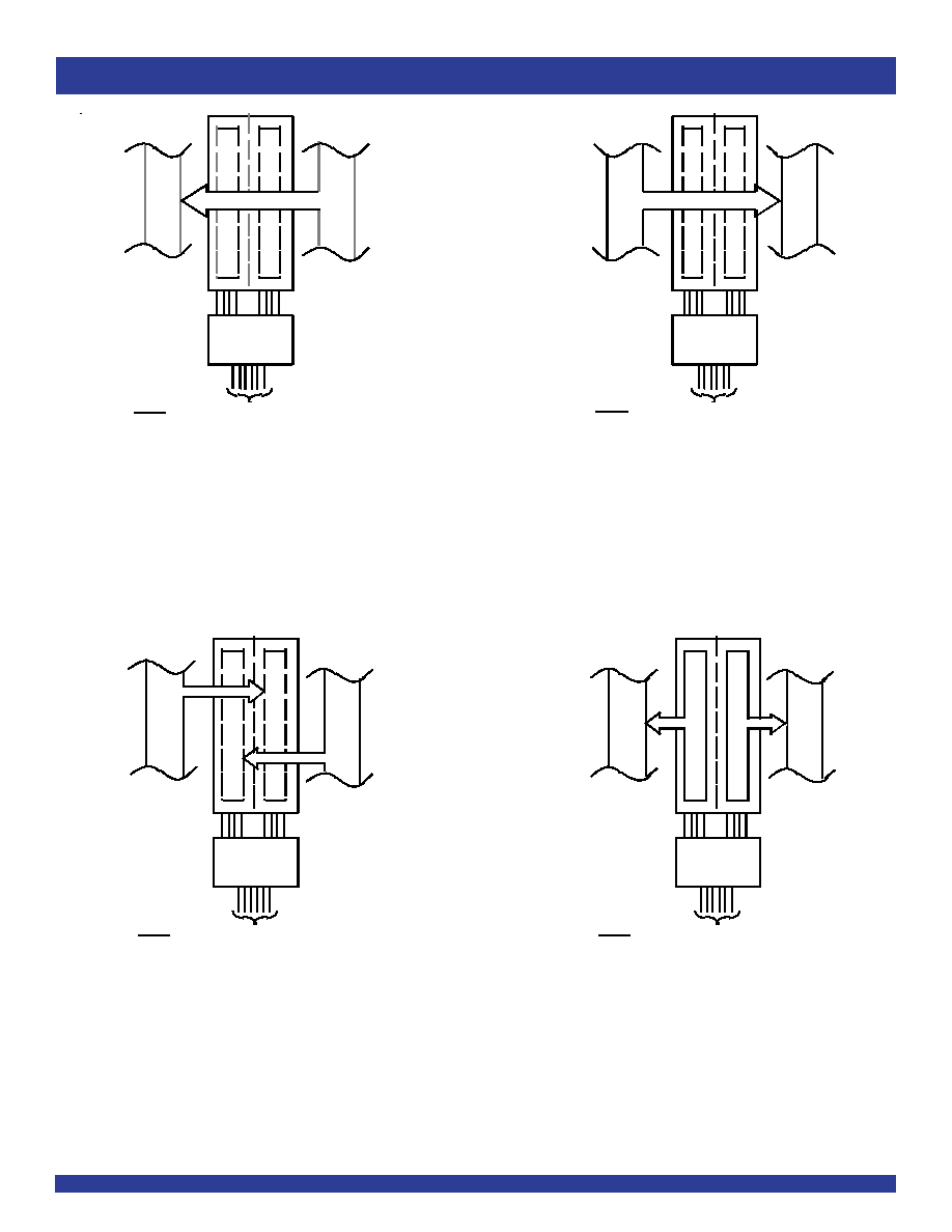
FUNCTION TABLE
(1)
Inputs
Data I/O
GAB
GBA
CPAB
CPBA
SAB
SBA
A
1
- A
8
B
1
- B
8
Operation
H
X
H or L
H or L
X
X
Input
Input
Isolation
H
X
X
X
Store A and B Data
X
H
H or L
X
X
Input
Unspecified
(2)
Store A, Hold B
H
H
X
X
Input
Output
Store A in Both Registers
L
X
H or L
X
X
Unspecified
(2)
Input
Hold A, Store B
L
L
X
X
Output
Input
Store B in Both Registers
L
L
X
X
X
L
Output
Input
Real-Time B Data to A Bus
L
L
X
H or L
X
H
Stored B Data to A Bus
L
H
X
X
L
X
Input
Output
Real-Time A Data to B Bus
L
H
H or L
X
H
X
Stored A Data to B Bus
H
L
H or L
H or L
H
H
Output
Output
Stored A Data to B Bus
Stored B Data to A Bus
INDUSTRIAL TEMPERATURE RANGE
4
IDT74FCT2652AT/CT
FAST CMOS OCTAL TRANSCEIVER/REGISTER (3-STATE)
G AB
G BA
C PAB
C PBA
SAB
SBA
L
L
X
X
X
L
BU S
B
BU S
A
BU S
A
BU S
B
G AB
G BA
C PAB
C PBA
SAB
SBA
H
H
X
X
L
X
BU S
A
BU S
B
G AB
G BA
C PAB
C PBA
SAB
SBA
X
H
X
X
X
L
X
X
X
X
L
H
X
X
BU S
A
BU S
B
GAB
G BA
C PAB
C PBA
SAB
SBA
H
L
H or
H or
H
H
Real-Time Transfer Bus B to A
Storage From A and/or B
Real-Time Transfer Bus A to B
Transfer Stored Data to A and/or B

INDUSTRIAL TEMPERATURE RANGE
IDT74FCT2652AT/CT
FAST CMOS OCTAL TRANSCEIVER/REGISTER (3-STATE)
5
Symbol
Parameter
Test Conditions
(1)
Min.
Typ.
(2)
Max.
Unit
V
IH
Input HIGH Level
Guaranteed Logic HIGH Level
2
--
--
V
V
IL
Input LOW Level
Guaranteed Logic LOW Level
--
--
0.8
V
I
IH
Input HIGH Current
(4)
V
CC
= Max.
V
I
= 2.7V
--
--
±1
µA
I
IL
Input LOW Current
(4)
V
CC
= Max.
V
I
= 0.5V
--
--
±1
µA
I
OZH
High Impedance Output Current
V
CC
= Max
V
O
= 2.7V
--
--
±1
µA
I
OZL
(3-State output pins)
(4)
V
O
= 0.5V
--
--
±1
I
I
Input HIGH Current
(4)
V
CC
= Max., V
I
= V
CC
(Max.)
--
--
±1
µA
V
IK
Clamp Diode Voltage
V
CC
= Min, I
IN
= -18mA
--
≠0.7
≠1.2
V
V
H
Input Hysteresis
--
--
200
--
mV
I
CC
Quiescent Power Supply Current
V
CC
= Max., V
IN
= GND or V
CC
--
0.01
1
µA
DC ELECTRICAL CHARACTERISTICS OVER OPERATING RANGE
Following Conditions Apply Unless Otherwise Specified:
Industrial: T
A
= ≠40∞C to +85∞C, V
CC
= 5.0V ±5%
NOTES:
1. For conditions shown as Min. or Max., use appropriate value specified under Electrical Characteristics for the applicable device type.
2. Typical values are at V
CC
= 5.0V, +25∞C ambient.
3. Not more than one output should be tested at one time. Duration of the test should not exceed one second.
4. The test limit for this parameter is ±5µA at T
A
= ≠55∞C.
Symbol
Parameter
Test Conditions
(1)
Min.
Typ.
(2)
Max.
Unit
I
ODL
Output LOW Current
V
CC
= 5V, V
IN
= V
IH
or V
IL
, V
OUT
= 1.5V
(3)
16
48
--
mA
I
ODH
Output HIGH Current
V
CC
= 5V, V
IN
= V
IH
or V
IL
, V
OUT
= 1.5V
(3)
≠16
≠48
--
mA
V
OH
Output HIGH Voltage
V
CC
= Min
I
OH
= ≠15mA
2.4
3.3
--
V
V
IN
= V
IH
or V
IL
V
OL
Output LOW Voltage
V
CC
= Min
I
OL
= 12mA
--
0.3
0.5
V
V
IN
= V
IH
or V
IL
OUTPUT DRIVE CHARACTERISTICS

INDUSTRIAL TEMPERATURE RANGE
6
IDT74FCT2652AT/CT
FAST CMOS OCTAL TRANSCEIVER/REGISTER (3-STATE)
Symbol
Parameter
Test Conditions
(1)
Min.
Typ.
(2)
Max.
Unit
I
CC
Quiescent Power Supply Current
V
CC
= Max.
--
0.5
2
mA
TTL Inputs HIGH
V
IN
= 3.4V
(3)
I
CCD
Dynamic Power Supply
V
CC
= Max.
V
IN
= V
CC
--
0.06
0.12
mA/
Current
(4)
Outputs Open
V
IN
= GND
MHz
GAB = GBA = GND
One Input Toggling
50% Duty Cycle
I
C
Total Power Supply Current
(6)
V
CC
= Max.
V
IN
= V
CC
--
0.6
2.2
mA
Outputs Open
V
IN
= GND
f
CP
= 10MHz
50% Duty Cycle
GAB = GBA = GND
V
IN
= 3.4V
--
1.1
4.2
One Bit Toggling
V
IN
= GND
at fi = 5MHz
50% Duty Cycle
V
CC
= Max.
V
IN
= V
CC
--
1.5
4
(5)
Outputs Open
V
IN
= GND
f
CP
= 10MHz
50% Duty Cycle
GAB = GBA = GND
V
IN
= 3.4V
--
3.8
13
(5)
Eight Bits Toggling
V
IN
= GND
at fi = 2.5MHz
50% Duty Cycle
NOTES:
1. For conditions shown as Min. or Max., use appropriate value specified under Electrical Characteristics for the applicable device type.
2. Typical values are at V
CC
= 5.0V, +25∞C ambient.
3. Per TTL driven input; (V
IN
= 3.4V). All other inputs at V
CC
or GND.
4. This parameter is not directly testable, but is derived for use in Total Power Supply Calculations.
5. Values for these conditions are examples of
I
CC
formula. These limits are guaranteed but not tested.
6. I
C
= I
QUIESCENT
+ I
INPUTS
+ I
DYNAMIC
I
C
= I
CC
+
I
CC
D
H
N
T
+ I
CCD
(f
CP
/2+ f
i
N
i
)
I
CC
= Quiescent Current
I
CC
= Power Supply Current for a TTL High Input (V
IN
= 3.4V)
D
H
= Duty Cycle for TTL Inputs High
N
T
= Number of TTL Inputs at D
H
I
CCD
= Dynamic Current caused by an Input Transition Pair (HLH or LHL)
f
CP
= Clock Frequency for Register Devices (Zero for Non-Register Devices)
f
i
= Output Frequency
N
i
= Number of Outputs at f
i
All currents are in milliamps and all frequencies are in megahertz.
POWER SUPPLY CHARACTERISTICS
INDUSTRIAL TEMPERATURE RANGE
IDT74FCT2652AT/CT
FAST CMOS OCTAL TRANSCEIVER/REGISTER (3-STATE)
7
NOTES:
1. See test circuit and waveforms.
2. Minimum limits are guaranteed but not tested on Propagation Delays.
3. This parameter is guaranteed but not tested.
FCT2652AT
FCT2652CT
Symbol
Parameter
Condition
(1)
Min.
(2)
Max.
Min.
(2)
Max.
Unit
t
PLH
Propagation Delay
C
L
= 50pF
2
6.3
1.5
5.4
ns
t
PHL
Bus to Bus
R
L
= 500
t
PZH
Output Enable Time
2
9.8
1.5
7.8
ns
t
PZL
GAB, GBA to Bus
t
PHZ
Output Disable Time
2
6.3
1.5
6.3
ns
t
PLZ
GAB, GBA to Bus
t
PLH
Propagation Delay
2
6.3
1.5
5.7
ns
t
PHL
Clock to Bus
t
PLH
Propagation Delay
2
7.7
1.5
6.2
ns
t
PHL
SBA or SAB to Bus
t
SU
Set-up Time, HIGH or LOW
2
--
2
--
ns
Bus to Clock
t
H
Hold Time, HIGH or LOW
1.5
--
1.5
--
ns
Bus to Clock
t
W
Clock Pulse Width
5
--
5
--
ns
HIGH or LOW
(3)
SWITCHING CHARACTERISTICS OVER OPERATING RANGE

INDUSTRIAL TEMPERATURE RANGE
8
IDT74FCT2652AT/CT
FAST CMOS OCTAL TRANSCEIVER/REGISTER (3-STATE)
Pulse
G enerator
R
T
D.U.T.
V
CC
V
IN
C
L
V
OU T
50pF
500
500
7.0V
3V
1.5V
0V
3V
1.5V
0V
3V
1.5V
0V
3V
1.5V
0V
DATA
IN PUT
TIM ING
INPUT
ASYNC HR O NOU S C ON TROL
PRES ET
C LEAR
ETC.
SYN CH RON OUS C ONTR OL
t
S U
t
H
t
RE M
t
S U
t
H
H IGH-LOW -HIG H
PULSE
LOW -H IGH -LOW
PULSE
t
W
1.5V
1.5V
SAM E PH ASE
IN PU T TR AN SITION
3V
1.5V
0V
1.5V
V
O H
t
PL H
O UTPUT
OPPOSITE PH ASE
IN PU T TR AN SITION
3V
1.5V
0V
t
P LH
t
P H L
t
P H L
V
O L
C ONTR OL
INPU T
3V
1.5V
0V
3.5V
0V
OUTPU T
N ORM A LLY
LOW
OUTPU T
N ORM A LLY
H IGH
SW ITCH
CLO SE D
SW ITC H
OPEN
V
O L
0.3V
0.3V
t
PLZ
t
PZL
t
P ZH
t
PH Z
3.5V
0V
1.5V
1.5V
EN AB LE
DISA BLE
V
O H
PRES ET
C LEAR
CLOCK ENABLE
ETC.
Octal link
Octal link
Octal link
Octal link
Octal link
TEST CIRCUITS AND WAVEFORMS
Propagation Delay
Test Circuits for All Outputs
Enable and Disable Times
Set-Up, Hold, and Release Times
Pulse Width
NOTES:
1. Diagram shown for input Control Enable-LOW and input Control Disable-HIGH.
2. Pulse Generator for All Pulses: Rate
1.0MHz; t
F
2.5ns; t
R
2.5ns.
Test
Switch
Open Drain
Disable Low
Closed
Enable Low
All Other Tests
Open
SWITCH POSITION
DEFINITIONS:
C
L
= Load capacitance: includes jig and probe capacitance.
R
T
= Termination resistance: should be equal to Z
OUT
of the Pulse Generator.

INDUSTRIAL TEMPERATURE RANGE
IDT74FCT2652AT/CT
FAST CMOS OCTAL TRANSCEIVER/REGISTER (3-STATE)
9
ORDERING INFORMATION
IDT XX FCT
Temperature
Range
XXXX
Device Type
X
Package
SO
Q
2652AT
2652CT
Small Outline IC
Quarter-size Small Outline Package
Octal Transceiver/Register (3-State)
74
- 40∞C to +85∞C
CORPORATE HEADQUARTERS
for SALES:
for Tech Support:
2975 Stender Way
800-345-7015 or 408-727-6116
logichelp@idt.com
Santa Clara, CA 95054
fax: 408-492-8674
(408) 654-6459
www.idt.com