 | –≠–ª–µ–∫—Ç—Ä–æ–Ω–Ω—ã–π –∫–æ–º–ø–æ–Ω–µ–Ω—Ç: 74FCT3807 | –°–∫–∞—á–∞—Ç—å:  PDF PDF  ZIP ZIP |
1
IDT74FCT3807/A
3.3V CMOS 1-TO-10 CLOCK DRIVER
COMMERCIAL/INDUSTRIAL TEMPERATURE RANGES
SEPTEMBER 2001
2001 Integrated Device Technology, Inc.
DSC-4647/2
c
IDT74FCT3807/A
COMMERCIAL/INDUSTRIAL TEMPERATURE RANGES
3.3V CMOS
1-TO-10 CLOCK DRIVER
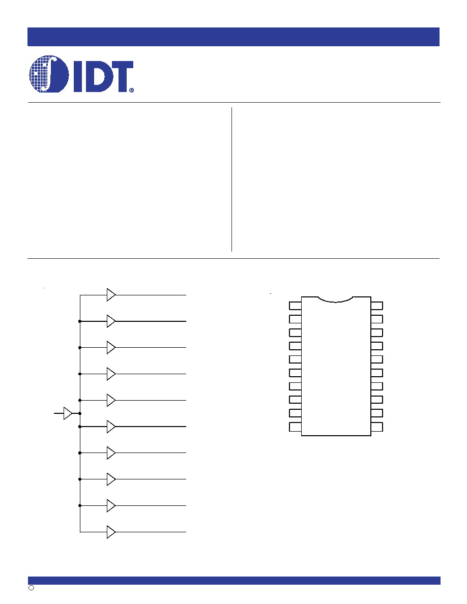
DESCRIPTION:
The FCT3807/A 3.3V clock driver is built using advanced dual metal CMOS
technology. This low skew clock driver offers 1:10 fanout. The large fanout from
a single input reduces loading on the preceding driver and provides an efficient
clock distribution network. The FCT3807/A offers low capacitance inputs with
hysteresis for improved noise margins. Multiple power and grounds reduce
noise. Typical applications are clock and signal distribution.
FUNCTIONAL BLOCK DIAGRAM
IN
O
1
O
2
O
3
O
4
O
5
O
6
O
7
O
8
O
9
O
10
PIN CONFIGURATION
GND
V
CC
GND
V
CC
GND
GND
V
CC
GND
O
5
V
CC
IN
O
1
O
2
O
3
O
4
O
10
O
9
O
8
O
7
O
6
1
2
3
4
5
6
7
8
9
10
11
12
13
14
15
16
17
18
19
20
SOIC/ SSOP/ QSOP
TOP VIEW
FEATURES:
∑ 0.5 MICRON CMOS Technology
∑ Guaranteed low skew < 350ps (max.)
∑ Very low duty cycle distortion < 350ps (max.)
∑ High speed: propagation delay < 3ns (max.)
∑ Very low CMOS power levels
∑ TTL compatible inputs and outputs
∑ 1:10 fanout
∑ Maximum output rise and fall time < 1.5ns (max.)
∑ Low input capacitance: 4.5pF typical
∑ V
CC
= 3.3V ± 0.3V
∑ Inputs can be driven from 3.3V or 5V components
∑ Available in SSOP, SOIC, and QSOP packages
The IDT logo is a registered trademark of Integrated Device Technology, Inc.

2
COMMERCIAL/INDUSTRIAL TEMPERATURE RANGES
IDT74FCT3807/A
3.3V CMOS 1-TO-10 CLOCK DRIVER
NOTES:
1. For conditions shown as Max. or Min., use appropriate value specified under Electrical Characteristics for the applicable device type.
2. Typical values are at V
CC
= 3.3V, +25∞C ambient.
3. Per TTL driven input (V
IN
= V
CC
-0.6V); all other inputs at V
CC
or GND.
4. This parameter is not directly testable, but is derived for use in Total Power Supply calculations.
5. Values for these conditions are examples of the I
C
formula. These limits are guaranteed but not tested.
6.
I
C
= I
QUIESCENT
+
I
INPUTS
+ I
DYNAMIC
I
C
= I
CC
+
I
CC
D
H
N
T
+ I
CCD
(f
i
)
I
CC
= Quiescent Current (I
CCL
, I
CCH
and I
CCZ
)
I
CC
= Power Supply Current for a TTL High Input (V
I
N
= V
CC
-0.6V)
D
H
= Duty Cycle for TTL Inputs High
N
T
= Number of TTL Inputs at D
H
I
CCD
= Dynamic Current Caused by an Input Transition Pair (HLH or LHL)
f
i
= Input Frequency
All currents are in milliamps and all frequencies are in megahertz.
ABSOLUTE MAXIMUM RATINGS
(1)
Symbol
Description
Max
Unit
V
TERM(2)
Terminal Voltage with Respect to GND
≠0.5 to +4.6
V
V
TERM(3)
Terminal Voltage with Respect to GND
≠0.5 to +7
V
V
TERM(4)
Terminal Voltage with Respect to GND
≠0.5 to V
CC
+0.5
V
T
STG
Storage Temperature
≠65 to +150
∞C
I
OUT
DC Output Current
≠60 to +60
mA
NOTES:
1. Stresses greater than those listed under ABSOLUTE MAXIMUM RATINGS may cause
permanent damage to the device. This is a stress rating only and functional operation
of the device at these or any other conditions above those indicated in the operational
sections of this specification is not implied. Exposure to absolute maximum rating
conditions for extended periods may affect reliability.
2. V
CC
terminals.
3. Input terminals.
4. Outputs and I/O terminals.
CAPACITANCE (T
A
= +25
O
C, f = 1.0MHz)
Symbol
Parameter
(1)
Conditions
Typ.
Max.
Unit
C
IN
Input Capacitance
V
IN
= 0V
4.5
6
pF
C
OUT
Output Capacitance
V
OUT
= 0V
5.5
8
pF
NOTE:
1. This parameter is measured at characterization but not tested.
PIN DESCRIPTION
Pin Names
Description
IN
Clock Inputs
Ox
Clock Outputs
POWER SUPPLY CHARACTERISTICS
Symbol
Parameter
Test Conditions
(1)
Min.
Typ.
(2)
Max.
Unit
I
CC
Quiescent Power Supply Current
V
CC
= Max.
--
10
30
µA
TTL Inputs HIGH
V
IN
= V
CC ≠
0.6V
(3)
I
CCD
Dynamic Power Supply Current
(4)
V
CC
= Max.
V
IN
= V
CC
--
0.31
0.45
mA/
Input toggling
V
IN
= GND
MHz
50% Duty Cycle
Outputs Open
I
C
Total Power Supply Current
(6)
V
CC
= Max.
V
IN
= V
CC
--
15.5
22.8
mA
Input toggling
V
IN
= GND
50% Duty Cycle
Outputs Open
V
IN
= V
CC ≠
0.6V
--
15.5
22.8
fi = 50MHz
V
IN
= GND

3
IDT74FCT3807/A
3.3V CMOS 1-TO-10 CLOCK DRIVER
COMMERCIAL/INDUSTRIAL TEMPERATURE RANGES
DC ELECTRICAL CHARACTERISTICS OVER OPERATING RANGE
Following Conditions Apply Unless Otherwise Specified
Commercial: T
A
= 0∞C to +75∞C, Industrial: T
A
= -40∞C to +85∞C, V
CC
= 3.3V ± 0.3V
Symbol
Parameter
Test Conditions
(1)
Min.
Typ.
Max.
Unit
V
IH
Input HIGH Level (Input pins)
Guaranteed Logic HIGH Level
2
--
5.5
V
Input HIGH Level (I/O pins)
2
--
V
CC
+ 0.5
V
IL
Input LOW Level (Input and I/O pins)
Guaranteed Logic LOW Level
≠0.5
--
0.8
V
I
IH
Input HIGH Current (Input pins)
V
CC
= Max.
V
I
= 5.5V
--
--
±1
Input HIGH Current (I/O pins)
V
I
= V
CC
--
--
±1
µA
I
IL
Input LOW Current (Input pins)
V
CC
= Max.
V
I
= GND
--
--
±1
Input LOW Current (I/O pins)
V
I
= GND
--
--
±1
I
OZH
High Impedence Output Current
V
CC
= Max.
V
O
= V
CC
--
--
±1
µA
I
OZL
(3-State Output Pins)
V
O
= GND
--
--
±1
V
IK
Clamp Diode Voltage
V
CC
= Min., I
IN
= ≠18mA
--
≠0.7
≠1.2
V
I
ODH
Output HIGH Current
V
CC
= 3.3V, V
IN
= V
IH
or V
IL
, V
O
= 1.5V
(3)
≠36
≠60
≠110
mA
I
ODL
Output LOW Current
V
CC
= 3.3V, V
IN
= V
IH
or V
IL
, V
O
= 1.5V
(3)
50
90
200
mA
V
OH
Output HIGH Voltage
V
CC
= Min.
I
OH
= ≠0.1mA
V
CC
≠0.2
--
--
V
V
IN
= V
IH
or V
IL
I
OH
= ≠8mA
2.4
(5)
3
--
V
OL
Output LOW Voltage
V
CC
= Min.
I
OL
= 0.1mA
--
--
0.2
V
IN
= V
IH
or V
IL
I
OL
= 16mA
--
0.2
0.4
V
I
OL
= 24mA
--
0.3
0.5
I
OFF
Input Power Off Leakage
V
CC
= 0V, V
IN
= 4.5V
--
--
±1
µA
I
OS
Short Circuit Current
(4)
V
CC
= Max., V
O
= GND
(3)
≠60
≠135
≠240
mA
V
H
Input Hysteresis
--
--
150
--
mV
I
CCL
Quiescent Power Supply Current
V
CC
= Max.
--
0.1
10
µA
I
CCH
V
IN
= GND or V
CC
I
CCZ
NOTES:
1. For conditions shown as Max. or Min., use appropriate value specified under Electrical Characteristics for the applicable device type.
2. Typical values are at Vcc = 3.3V, +25∞C ambient.
3. Not more than one output should be shorted at one time. Duration of the test should not exceed one second.
4. This parameter is guaranteed but not tested.
5. V
OH
= Vcc - 0.6V at rated current.
4
COMMERCIAL/INDUSTRIAL TEMPERATURE RANGES
IDT74FCT3807/A
3.3V CMOS 1-TO-10 CLOCK DRIVER
NOTES:
1. See test circuits and waveforms.
2. Minimum limits are guaranteed but not tested on Propagation Delays.
3. t
PLH
, t
PHL
, t
SK
(t) are production tested. All other parameters guaranteed but not production tested.
4. Propagation delay range indicated by Min. and Max. limit is due to V
CC
, operating temperature and process parameters. These propagation delay limits do not imply skew.
FCT3807
FCT3807A
Symbol
Parameter
Conditions
(1)
Min
.
(2)
Max
.
Min
.
(2)
Max
.
Unit
t
PLH
Propagation Delay
C
L
= 30pF
1.5
4.5
1.5
4
ns
t
PHL
f
67MHz
t
R
Output Rise Time
(See figure 3)
--
1.5
--
1.5
ns
t
F
Output Fall Time
--
1.5
--
1.5
ns
t
SK(O)
Output skew: skew between outputs of
--
0.5
--
0.35
ns
same package (same transition)
t
SK(P)
Pulse skew: skew between opposite transitions
--
0.5
--
0.35
ns
of same output (|t
PHL -≠
t
PLH
|)
t
SK(T)
Package skew: skew between outputs of different
--
1
--
0.75
ns
packages at same power supply voltage,
temperature, package type and speed grade
FCT3807
FCT3807A
Symbol
Parameter
Conditions
(1)
Min
.
(2)
Max
.
Min
.
(2)
Max
.
Unit
t
PLH
Propagation Delay
C
L
= 50pF
1.5
4.8
1.5
4.3
ns
t
PHL
f
40MHz
t
R
Output Rise Time
(See figure 4)
--
1.5
--
1.5
ns
t
F
Output Fall Time
--
1.5
--
1.5
ns
t
SK(O)
Output skew: skew between outputs of
--
0.5
--
0.35
ns
same package (same transition)
t
SK(P)
Pulse skew: skew between opposite transitions
--
0.5
--
0.35
ns
of same output (|t
PHL -≠
t
PLH
|)
t
SK(T)
Package skew: skew between outputs of different
--
1
--
0.75
ns
packages at same power supply voltage,
temperature, package type and speed grade
SWITCHING CHARACTERISTICS OVER OPERATING RANGE - COMMERCIAL
(3,4)
FCT3807
FCT3807A
Symbol
Parameter
Conditions
(1)
Min
.
(2)
Max
.
Min
.
(2)
Max
.
Unit
t
PLH
Propagation Delay
50
to V
CC
/2
1.5
3.5
1.5
3
ns
t
PHL
C
L
= 10pF
t
R
Output Rise Time
(See figure 1)
--
1.5
--
1.5
ns
t
F
Output Fall Time
or 10
AC
--
1.5
--
1.5
ns
t
SK(O)
Output skew: skew between outputs of
termination,
--
0.5
--
0.35
ns
same package (same transition)
C
L
= 50pF
t
SK(P)
Pulse skew: skew between opposite transitions
(See figure 2)
--
0.5
--
0.35
ns
of same output (|t
PHL -≠
t
PLH
|)
f
100MHz
t
SK(T)
Package skew: skew between outputs of different
Outputs
--
0.9
--
0.65
ns
packages at same power supply voltage,
connected in
temperature, package type and speed grade
groups of two

5
IDT74FCT3807/A
3.3V CMOS 1-TO-10 CLOCK DRIVER
COMMERCIAL/INDUSTRIAL TEMPERATURE RANGES
NOTES:
1. See test circuits and waveforms.
2. Minimum limits are guaranteed but not tested on Propagation Delays.
3. t
PLH
, t
PHL
, t
SK
(t) are production tested. All other parameters guaranteed but not production tested.
4. Propagation delay range indicated by Min. and Max. limit is due to V
CC
, operating temperature and process parameters. These propagation delay limits do not imply skew.
FCT3807
FCT3807A
Symbol
Parameter
Conditions
(1)
Min
.
(2)
Max
.
Min
.
(2)
Max
.
Unit
t
PLH
Propagation Delay
C
L
= 30pF
1.5
4.5
1.5
4
ns
t
PHL
f
67MHz
t
R
Output Rise Time
(See figure 3)
--
1.5
--
1.5
ns
t
F
Output Fall Time
--
1.5
--
1.5
ns
t
SK(O)
Output skew: skew between outputs of
--
0.6
--
0.45
ns
same package (same transition)
t
SK(P)
Pulse skew: skew between opposite transitions
--
0.6
--
0.45
ns
of same output (|t
PHL -≠
t
PLH
|)
t
SK(T)
Package skew: skew between outputs of different
--
1
--
0.75
ns
packages at same power supply voltage,
temperature, package type and speed grade
FCT3807
FCT3807A
Symbol
Parameter
Conditions
(1)
Min
.
(2)
Max
.
Min
.
(2)
Max
.
Unit
t
PLH
Propagation Delay
C
L
= 50pF
1.5
4.8
1.5
4.3
ns
t
PHL
f
40MHz
t
R
Output Rise Time
(See figure 4)
--
1.5
--
1.5
ns
t
F
Output Fall Time
--
1.5
--
1.5
ns
t
SK(O)
Output skew: skew between outputs of
--
0.6
--
0.45
ns
same package (same transition)
t
SK(P)
Pulse skew: skew between opposite transitions
--
0.6
--
0.45
ns
of same output (|t
PHL -≠
t
PLH
|)
t
SK(T)
Package skew: skew between outputs of different
--
1
--
0.75
ns
packages at same power supply voltage,
temperature, package type and speed grade
SWITCHING CHARACTERISTICS OVER OPERATING RANGE - INDUSTRIAL
(3,4)
FCT3807
FCT3807A
Symbol
Parameter
Conditions
(1)
Min
.
(2)
Max
.
Min
.
(2)
Max
.
Unit
t
PLH
Propagation Delay
50
to V
CC
/2
1.5
3.5
1.5
3
ns
t
PHL
C
L
= 10pF
t
R
Output Rise Time
(See figure 1)
--
1.5
--
1.5
ns
t
F
Output Fall Time
or 50
AC
--
1.5
--
1.5
ns
t
SK(O)
Output skew: skew between outputs of
termination,
--
0.6
--
0.45
ns
same package (same transition)
C
L
= 10pF
t
SK(P)
Pulse skew: skew between opposite transitions
(See figure 2)
--
0.6
--
0.45
ns
of same output (|t
PHL -≠
t
PLH
|)
f
100MHz
t
SK(T)
Package skew: skew between outputs of different
Outputs
--
0.9
--
0.65
ns
packages at same power supply voltage,
connected in
temperature, package type and speed grade
groups of two

6
COMMERCIAL/INDUSTRIAL TEMPERATURE RANGES
IDT74FCT3807/A
3.3V CMOS 1-TO-10 CLOCK DRIVER
D.U.T.
Pulse
Generator
V
IN
V
OUT
V
CC
R
T
V
CC
100
100
10pF
D.U.T.
Pulse
Generator
V
IN
V
OUT
V
CC
R
T
50
10pF
220pF
30pF
D.U.T.
Pulse
Generator
V
IN
V
OUT
V
CC
R
T
C
L
50pF
D.U.T.
Pulse
Generator
V
IN
V
OUT
V
CC
R
T
C
L
50pF
C
L
D.U.T.
Pulse
Generator
V
IN
V
OUT
V
CC
R
T
500
500
GND
6V
Figure 1. Z
O
= 50
to V
CC
/2, C
L
= 10pF
The capacitor value for ac termination is determined by the operating frequency. For very
low frequencies a higher capacitor value should be selected.
Figure 3. C
L
= 30pF Circuit
ENABLE AND DISABLE TIME
SWITCH POSITION
DEFINITIONS:
C
L
= Load capacitance: includes jig and probe capacitance.
R
T
= Termination resistance: should be equal to Z
OUT
of the Pulse Generator.
Figure 3. C
L
= 50pF Circuit
Figure 2. Z
O
= 50
AC Termination, C
L
= 10pF
Test
Switch
Disable LOW
6V
Enable LOW
Disable HIGH
GND
Enable HIGH
TEST CIRCUITS
Figure 5. Enable and Disable Time Circuit

7
IDT74FCT3807/A
3.3V CMOS 1-TO-10 CLOCK DRIVER
COMMERCIAL/INDUSTRIAL TEMPERATURE RANGES
t
PL H1
O UTPUT 1
O UTPUT 2
t
SK(o)
t
PL H2
3V
0V
V
O H
1.5V
1.5V
V
O L
V
O H
1.5V
V
O L
INPUT
t
PH L1
t
PHL2
t
SK(o )
t
SK(o)
=
|t
PLH2 -
t
PLH1
|
or
|t
PHL2 -
t
PHL1
|
CO NTRO L
INPUT
O UTPUT
N ORM ALLY
LOW
O UTPUT
N ORM ALLY
HIGH
3V
1.5V
0V
3.5V
0V
SW ITCH
CLOSE D
SW ITCH
O PEN
V
O L
V
O H
0.3V
0.3V
t
PLZ
t
PZL
t
PZH
t
PHZ
3.5V
0V
1.5V
1.5V
ENABLE
DISA BLE
3V
0V
V
O H
t
PL H
t
PHL
V
O L
1.5V
1.5V
t
R
t
F
2.0V
0.8V
IN PUT
OUTPU T
INPUT
t
PL H1
PACKAGE 1 OUTPUT
PACKAGE 2 OUTPUT
t
SK(t)
t
PLH2
3V
0V
V
O H
1.5V
1.5V
V
O L
V
O H
1.5V
V
O L
t
PH L1
t
PH L2
t
SK(t)
t
SK(t)
= |t
PLH2 -
t
PLH1
|
or
|t
PHL 2 -
t
PHL1
|
t
PLH
t
PH L
3V
0V
V
O H
1.5V
1.5V
V
O L
t
SK(p)
=
|t
PHL -
t
PLH
|
IN PU T
OUTPU T
TEST WAVEFORMS
Enable and Disable Times
Package 1 and Package 2 are same device type and speed grade
NOTES:
1. Diagram shown for input Control Enable-LOW and input Control Disable-HIGH
2. Pulse Generator for All Pulses: f
1.0MHz; t
F
2.5ns; t
R
2.5ns
Pulse Skew - t
SK(P)
Package Skew - t
SK(T)
Package Delay
Output Skew - t
SK(O)

8
COMMERCIAL/INDUSTRIAL TEMPERATURE RANGES
IDT74FCT3807/A
3.3V CMOS 1-TO-10 CLOCK DRIVER
ORDERING INFORMATION
IDT74FCT
Temp. Range
XXXX
Device Type
X
Package
1-to-10 3.3V Clock Driver
SO
PY
Q
3807
3807A
Small Outline IC
Shrink Small Outline IC
Quarter-size Small Outline IC
X
Blank
I
Commercial (0∞C to +70∞C)
Industrial (-40∞C to +85∞C)
CORPORATE HEADQUARTERS
for SALES:
for Tech Support:
2975 Stender Way
800-345-7015 or 408-727-6116
logichelp@idt.com
Santa Clara, CA 95054
fax: 408-492-8674
(408) 654-6459
www.idt.com