GTLP306.pmd
1
IDT74GTLP306
8-BIT LVTTL/GTLP BUS TRANSCEIVER
INDUSTRIAL TEMPERATURE RANGE
MAY 2002
2002 Integrated Device Technology, Inc.
DSC-5978/8
c
IDT74GTLP306
PRELIMINARY
INDUSTRIAL TEMPERATURE RANGE
8-BIT LVTTL/GTLP
BUS TRANSCEIVER
DESCRIPTION:
The GTLP306 is an 8-bit bus transceiver. It provides signal level
translation, from LVTTL to GTLP, for applications requiring a high-speed
interface between cards operating at LVTTL logic levels and back-planes
operating at GTLP logic levels. GTLP provides reduced output swing
(<1V), reduced input threshold levels, and output edge-rate control to
minimize signal setting times. The GTLP306 is a derivative of the Gunning
Transceiver Logic (GTL) JEDEC standard JESD8-3 and incorporates
internal edge-rate control, which is process, voltage, and temperature
(PVT) compensated.
The GTLP306 combines a transceiver function with an LVTTL to GTLP
translation. Data polarity is non-inverting, and the data flow direction is
controlled by the T/R pin. The outputs are enabled to allow data through
the device when OE is low. Otherwise, both A and B are placed in a high-
impedance state.
GTLP output low voltage is less than 0.5V. The output high is 1.5V, and
the receiver threshold is 1V.
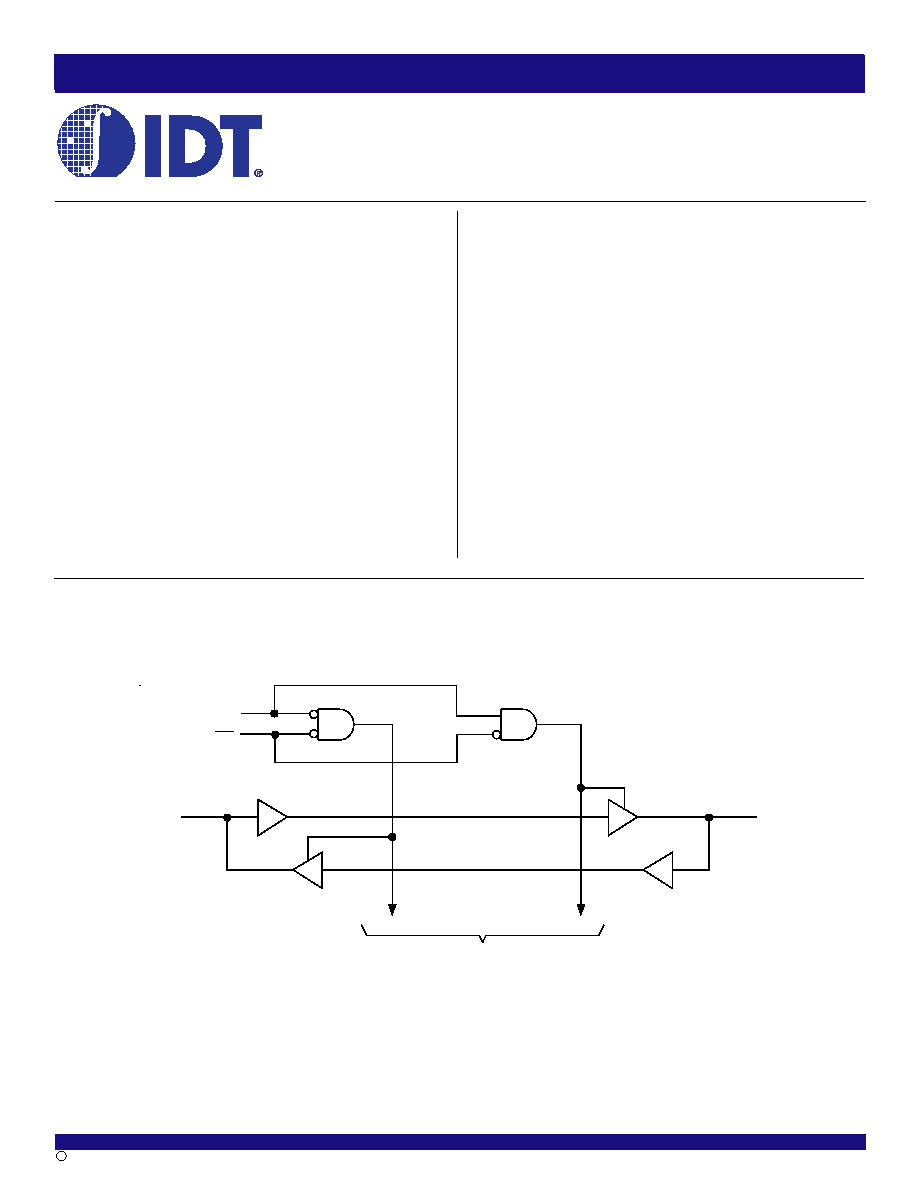
T / R
OE
A0 (LVTTL I/O)
B0 (GTLP I/O)
TO SEVEN OTHER CHANNELS
The IDT logo is a registered trademark of Integrated Device Technology, Inc.
FEATURES:
� Bidirectional interface between GTLP and LVTTL logic levels
� Edge Rate Control Circuit reduces output noise
� V
REF
pin provides reference voltage for receiver threshold
� CMOS technology for low power dissipation
� Special PVT Compensation circuitry to provide consistent perfor-
mance over variations of process, supply voltage, and temperature
� 5V tolerant inputs on LVTTL ports
� Bus-Hold to eliminate the need for external pull-up resistors for
unused inputs to A-Port
� Power up/down and power-off high-impedance for live insertion
� TTL-compatible Driver and Control inputs
� High Output source/sink �24mA on A-Port pins
� Flow-through architecture optimizes system layout
� Open drain on GTLP to support wired OR connection
� ESD performance of >2000V
� Available in TSSOP package
FUNCTIONAL BLOCK DIAGRAM
2
INDUSTRIAL TEMPERATURE RANGE
IDT74GTLP306
8-BIT LVTTL/GTLP BUS TRANSCEIVER
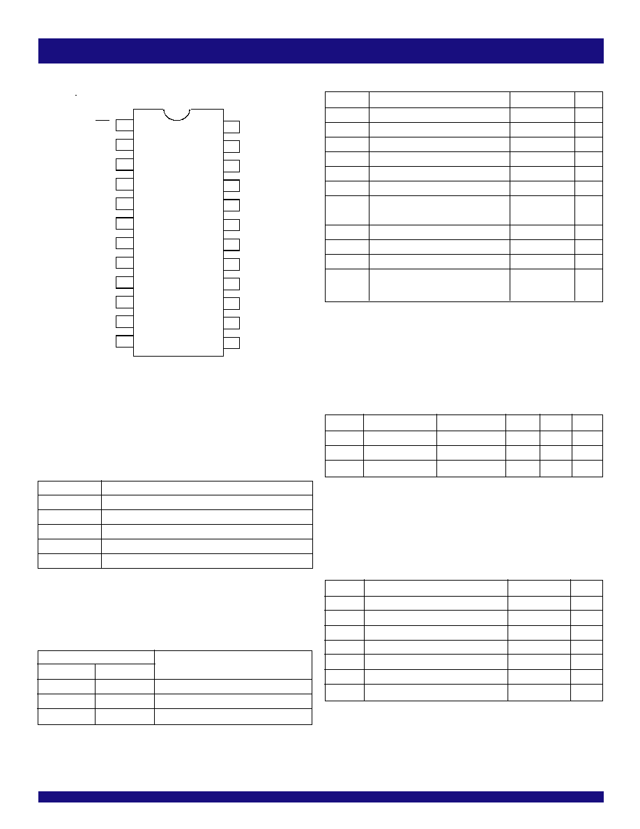
TSSOP
TOP VIEW
PIN CONFIGURATION
OE
A
0
A
1
GND
A
7
2
3
4
5
6
7
8
9
10
11
12
13
14
15
16
17
18
19
20
21
22
23
24
1
V
CC
A
2
A
3
A
4
A
5
A
6
GND
T/
R
B
1
B
0
B
7
V
REF
B
2
B
3
B
4
B
5
B
6
GND
GND
ABSOLUTE MAXIMUM RATINGS
(1,2)
Symbol
Rating
Max.
Unit
V
CC
Supply Voltage
�0.5 to +7
V
V
I
DC Input Voltage
�0.5 to +7
V
V
O
DC Output Voltage, 3-State
�0.5 to +7
V
V
O
DC Output Voltage, Active
�0.5 to +7
V
I
OL
DC Output Sink Current into A-port
48
mA
I
OH
DC Output Source Current from A-port
�48
mA
I
OL
DC Output Sink Current into B-port
100
mA
(in the LOW state)
I
IK
DC Input Diode Current V
I
< 0V
�50
mA
I
OK
DC Output Diode Current V
O
< 0V
�50
mA
I
OK
DC Output Diode Current V
O
> V
CC
+50
mA
T
STG
Storage Temperature
�65 to +150
�C
NOTES:
1. Stresses greater than those listed under ABSOLUTE MAXIMUM RATINGS may cause
permanent damage to the device. This is a stress rating only and functional operation
of the device at these or any other conditions above those indicated in the operational
sections of this specification is not implied. Exposure to absolute maximum rating
conditions for extended periods may affect reliability.
2. Unused inputs without Bus-Hold must be held HIGH or LOW.
CAPACITANCE
(T
A
= +25�C, f = 1.0MH
Z
)
Symbol
Parameter
(1)
Conditions
Typ.
(2)
Max.
Unit
C
IN
Control Pins
V
I
= V
CCQ
or 0
5
--
pF
C
I
/
O
A-Port
V
I
= V
CCQ
or 0
7
--
pF
C
I
/
O
B-Port
V
I
= V
CCQ
or 0
9
--
pF
NOTES:
1. As applicable to the device type.
2. All typical values are at V
CC
= 3.3V.
RECOMMENDED OPERATING
CONDITIONS
(1)
Symbol
Rating
Recommended
Unit
V
CC
Supply Voltage
3.15 to 3.45
V
V
TT
Bus Termination Voltage
1.35 to 1.65
V
V
I
Input Voltage on A-Port and Control Pins
0 to 5.5
V
I
OH
HIGH Level Output Current (A-Port)
-24
mA
I
OL
LOW Level Output Current (A-Port)
+24
mA
I
OL
LOW Level Output Current (B-Port)
50
mA
T
A
Operating Temperature
�40 to +85
�C
NOTE:
1. Unused inputs without Bus-Hold must be held HIGH or LOW.
FUNCTION TABLE
(1)
Inputs
OE
T/R
Output
H
X
High Z on Bus A and Bus B
L
L
Bus B Data to Bus A
L
H
Bus A Data to Bus B
NOTE:
1. H = HIGH Voltage Level
X = Don't Care
L = LOW Voltage Level
NOTE:
1. A-Port pins have Bus-Hold. All other pins are standard input, output, or I/O.
PIN DESCRIPTION
Pin Names
Description
(1)
OE
Output Enable (Active LOW)
T/R
Transmit/Receive Input
V
REF
GTLP Input Reference Voltage
A
0
- A
7
Side A Inputs or 3-State Outputs
B
0
- B
7
Side B Inputs or 3-State Outputs
3
IDT74GTLP306
8-BIT LVTTL/GTLP BUS TRANSCEIVER
INDUSTRIAL TEMPERATURE RANGE
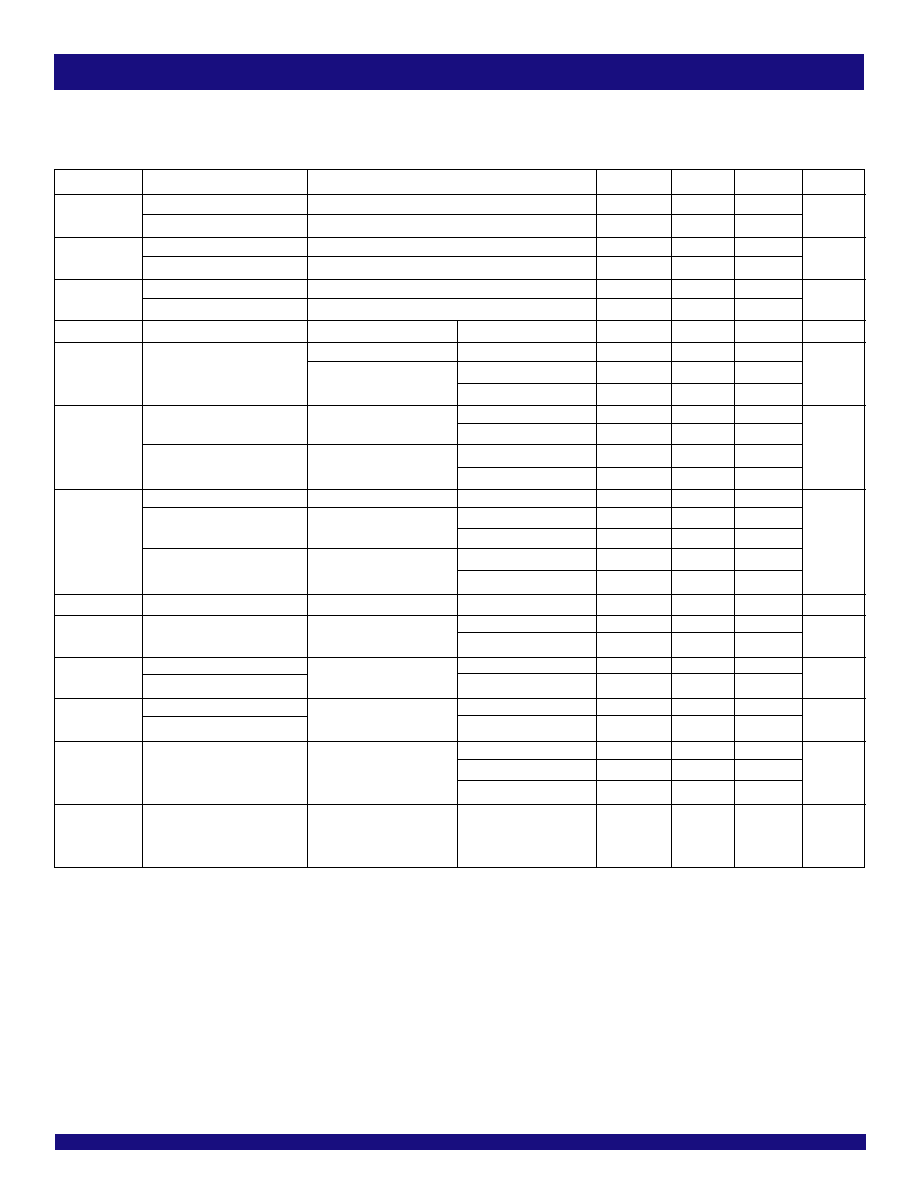
DC ELECTRICAL CHARACTERISTICS OVER OPERATING RANGE
Following Conditions Apply Unless Otherwise Specified:
Industrial: T
A
= �40�C to +85�C, V
REF
= 1V, V
CC
= 3.3V � 5%
Symbol
Parameter
Test Conditions
Min.
Typ.
(1)
Max.
Unit
V
IH
B-Port
--
V
REF
+ 0.05
--
V
TT
V
All Other ports
--
2
--
--
V
IL
B-Port
--
0
--
V
REF
� 0.05
V
All Other ports
--
--
--
0.8
V
REF
GTLP
--
--
1
--
V
GTL
--
--
0.8
--
V
IK
--
V
CC
= 3.15V
I
I
= �18mA
--
--
�1.2
V
A-Port
V
CC
= Min to Max
(2)
I
OH
= �100�A
V
CC
�0.2
--
--
V
OH
V
CC
= 3.15V
I
OH
= �12mA
2.4
--
--
V
I
OH
= �24mA
2
--
--
A-Port
V
CC
= Min to Max
(2)
I
OL
= 100�A
--
--
0.2
V
OL
V
CC
= 3.15V
I
OL
= 24mA
--
--
0.5
V
B-Port
V
CC
= 3.15V
I
OL
= 40mA
--
--
0.4
I
OL
= 50mA
--
--
0.55
Control Pins
V
CC
= 3.45V
V
I
= 5.5V or 0V
--
--
�5
A-Port
V
CC
= 3.45V
V
I
= 5.5V
--
--
20
I
I
V
I
= 0
--
--
�20
�A
B-Port
V
CC
= 3.45V
V
I
= V
TT
--
--
5
V
I
= 0
--
--
�5
I
OFF
A-Port
V
CC
= 0
V
I
or V
O
= 0 to 4.5V
--
--
100
�A
I
I
(HOLD)
A-Port
V
CC
= 3.15V
V
I
= 0.8V
75
--
--
�A
V
I
= 2V
�20
--
--
I
OZH
A-Port
V
CC
= 3.45V
V
O
= 3.45 V
--
--
20
�A
B-Port
V
O
= 1.5V
--
--
5
I
OZL
A-Port
V
CC
= 3.45V
V
O
= 0
--
--
�20
�A
B-Port
V
O
= 0.55V
--
--
�5
V
CC
= 3.45V
Outputs HIGH
--
7
18
I
CC
(V
CC
)
A or B Ports
I
O
= 0
Outputs LOW
--
8
20
mA
V
I
= V
CC
or GND
Outputs Disabled
--
8
20
I
CC
(3)
A-Port and Control Pins
V
CC
= 3.45V
One Input at V
CC
- 0.6V
--
0
1
mA
A or Control Inputs at
V
CC
or GND
NOTES:
1. All typical values are at V
CC
= 3.3V and T
A
= 25�C.
2. For conditions shown as Max. or Min., use appropriate value specified under Recommended Operating Conditions.
3.
I
CC
is the increase in supply current for each input that is at the specified LVTTL voltage level rather than V
CC
or GND.
4
INDUSTRIAL TEMPERATURE RANGE
IDT74GTLP306
8-BIT LVTTL/GTLP BUS TRANSCEIVER
NOTES:
1. See Test Circuits and Waveforms. T
A
= �40�C to +85�C.
2. Unless otherwise noted, V
REF
= 1V.
3. Typical values are at V
CC
= 3.3V and T
A
= 25�C.
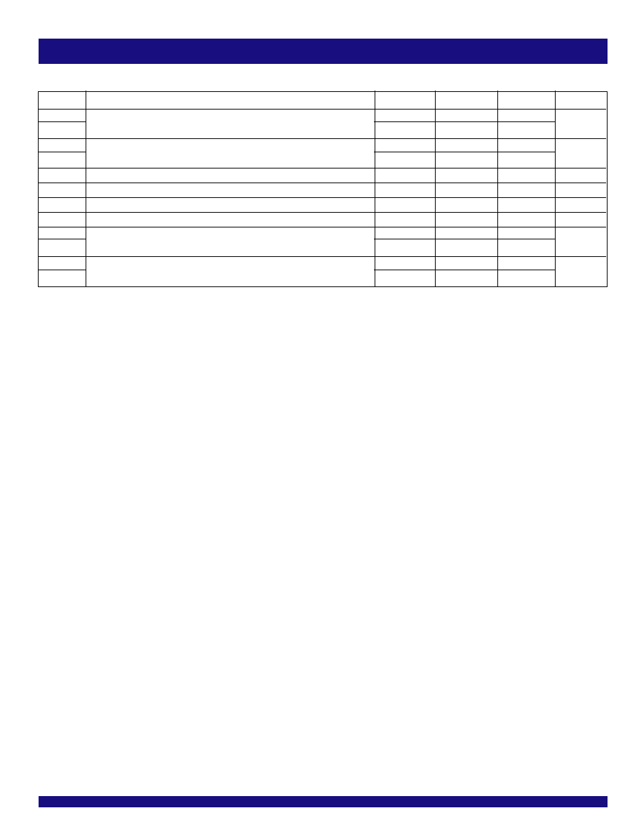
SWITCHING CHARACTERISTICS OVER OPERATING RANGE
(1,2)
Symbol
Parameter
Min.
Typ.
(3)
Max.
Unit
t
PLH
Ax to Bx
1
4
7.5
ns
t
PHL
1
5.1
7.5
t
PLH
Bx to Ax
1
5.8
8.3
ns
t
PHL
1
4.9
8.3
t
RISE
Transition Time, B outputs (20% to 80%)
--
2.6
--
ns
t
FALL
Transition Time, B outputs (20% to 80%)
--
2.6
--
ns
t
RISE
Transition Time, A outputs (10% to 90%)
--
2.5
--
ns
t
FALL
Transition Time, A outputs (10% to 90%)
--
2.5
--
ns
t
PZH,
t
PZL
OE to Ax
1
4.5
9.5
ns
t
PHZ,
t
PLZ
1
4.9
9.5
t
PLH
OE to Bx
1
5.4
9.5
ns
t
PHL
1
6
9.5
5
IDT74GTLP306
8-BIT LVTTL/GTLP BUS TRANSCEIVER
INDUSTRIAL TEMPERATURE RANGE
6V
Open
GND
INPUT
Vm V
3V
0V
Vm V
t
W
500
C
L
= 50pF
500
25
30pF
FROM
OUTPUT
UNDER
TEST
1.5V (GTLP)
1.2V (GTL)
FROM
OUTPUT
UNDER
TEST
S
(1)
(1)
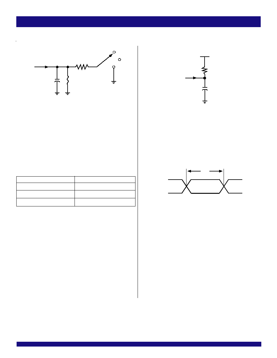
TEST CIRCUITS AND WAVEFORMS
Test Circuit for A Outputs
(1)
NOTE:
1. C
L
includes probes and jig capacitance. For B-Port outputs, C
L
= 30pF is used for
worst case edge rate.
NOTE:
1. C
L
includes probes and jig capacitance.
NOTE:
All input pulses have the following characteristics: frequency = 10 MHz, t
R
= t
F
= 2 ns, Z
O
= 50
. The outputs are measured one at a time with one transition per measurement.
Test Circuit for B Outputs
(1)
Voltage Waveforms Pulse Duration
(Vm = V
CC
/2 for A-Port, 1V for GTLP B-Port, and 0.8V for GTL
B-Port)
SWITCH POSITION
Test
Switch
t
PLH
/ t
PHL
Open
t
PHZ
/ t
PZH
GND
t
PLZ
/ t
PZL
6V
NOTE:
1. 1.5V for B-Port GTLP.
1.2V for B-Port GTL.