 | –≠–ª–µ–∫—Ç—Ä–æ–Ω–Ω—ã–π –∫–æ–º–ø–æ–Ω–µ–Ω—Ç: 74LVC112A | –°–∫–∞—á–∞—Ç—å:  PDF PDF  ZIP ZIP |

INDUSTRIAL TEMPERATURE RANGE
IDT74LVC112A
3.3V CMOS DUAL NEGATIVE-EDGE-TRIGGERED J-K FLIP-FLOP
1
MAY 1999
INDUSTRIAL TEMPERATURE RANGE
The IDT logo is a registered trademark of Integrated Device Technology, Inc.
©1999 Integrated Device Technology, Inc.
DSC-4770/2
FEATURES:
∑ 0.5 MICRON CMOS Technology
∑ ESD > 2000V per MIL-STD-883, Method 3015; > 200V using
machine model (C = 200pF, R = 0)
∑ V
CC
= 3.3V ± 0.3V, Normal Range
∑ V
CC
= 2.7V to 3.6V, Extended Range
∑ CMOS power levels (0.4
µµ
µµ
µ W typ. static)
∑ Rail-to-Rail output swing for increased noise margin
∑ All inputs, outputs, and I/Os are 5V tolerant
∑ Supports hot insertion
∑ Available in QSOP, SOIC, SSOP, and TSSOP packages
FUNCTIONAL BLOCK DIAGRAM
DRIVE FEATURES:
∑ High Output Drivers: ±24mA
∑ Reduced system switching noise
APPLICATIONS:
∑ 5V and 3.3V mixed voltage systems
∑ Data communication and telecommunication systems
IDT74LVC112A
DESCRIPTION:
This dual negative-edge-triggered J-K flip-flop is built using advanced
dual metal CMOS technology. A low level at the preset (PRE) or clear (CLR)
inputs sets or resets the outputs, regardless of the levels of the other inputs.
When PRE and CLR are inactive (high), data at the J and K inputs meeting
the setup time requirements is transferred to the outputs on the negative-
going edge of the clock pulse. Clock triggering occurs at a voltage level and
is not directly related to the rise time of the clock pulse. Following the hold-
time interval, data at the J and K inputs can be changed without affecting the
levels at the outputs. The LVC112A can perform as a toggle flip-flop by tying
J and K high.
Inputs can be driven from either 3.3V or 5V devices. This feature allows
the use of this device as a translator in a mixed 3.3V/5V supply system.
The LVC112A has been designed with a ±24mA output driver. This
driver is capable of driving a moderate to heavy load while maintaining
speed performance.
3.3V CMOS DUAL
NEGATIVE-EDGE-TRIGGERED
J-K FLIP-FLOP WITH CLEAR
AND PRESET, 5 VOLT TOLERANT I/O
Q
CLR
J
K
PRE
Q
CLK

INDUSTRIAL TEMPERATURE RANGE
2
IDT74LVC112A
3.3V CMOS DUAL NEGATIVE-EDGE-TRIGGERED J-K FLIP-FLOP
NOTE:
1. As applicable to the device type.
Symbol
Parameter
(1)
Conditions
Typ.
Max.
Unit
C
IN
Input Capacitance
V
IN
= 0V
4.5
6
pF
C
OUT
Output Capacitance
V
OUT
= 0V
5.5
8
pF
C
I/O
I/O Port Capacitance
V
IN
= 0V
6.5
8
pF
CAPACITANCE
(T
A
= +25∞C, F = 1.0MHz)
Symbol
Description
Max
Unit
V
TERM
Terminal Voltage with Respect to GND
≠0.5 to +6.5
V
T
STG
Storage Temperature
≠65 to +150
∞C
I
OUT
DC Output Current
≠50 to +50
mA
I
IK
Continuous Clamp Current,
≠50
mA
I
OK
V
I
< 0 or V
O
< 0
I
CC
Continuous Current through each
±100
mA
I
SS
V
CC
or GND
ABSOLUTE MAXIMUM RATINGS
(1)
NOTE:
1. Stresses greater than those listed under ABSOLUTE MAXIMUM RATINGS may cause
permanent damage to the device. This is a stress rating only and functional operation
of the device at these or any other conditions above those indicated in the operational
sections of this specification is not implied. Exposure to absolute maximum rating
conditions for extended periods may affect reliability.
QSOP/ SOIC/ SSOP/ TSSOP
TOP VIEW
PIN CONFIGURATION
2
3
4
5
6
7
8
9
10
11
12
13
14
15
16
1
V
CC
1
CLK
1
K
1
CLR
1
J
1
Q
1
Q
2
Q
GND
2
K
2
J
2
Q
2
CLR
2
CLK
2
PRE
1
PRE
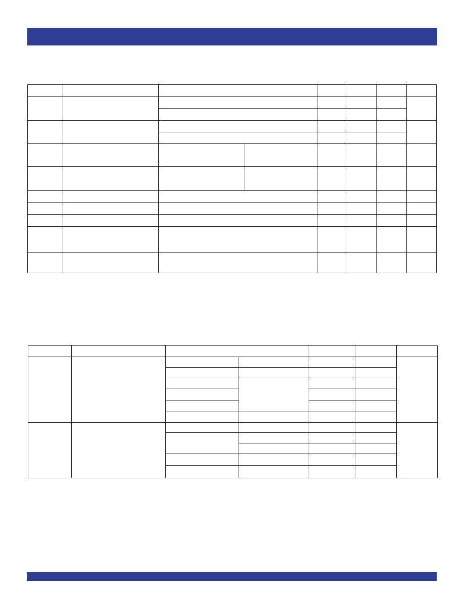
PIN DESCRIPTION
Pin Names
Description
xCLK
CLK Inputs
xCLR
Clear Inputs (Active LOW)
xPRE
Preset Inputs (Active LOW)
xJ, xK
Data Inputs
xQ, xQ
Data Outputs
FUNCTION TABLE
(1)
Inputs
Outputs
xPRE
xCLR
xCLK
xJ
xK
xQ
xQ
L
H
X
X
X
H
L
H
L
X
X
X
L
H
L
L
X
X
X
H
(2)
H
(2)
H
H
L
L
Q
(3)
Q
(4)
H
H
H
L
H
L
H
H
L
H
L
H
H
H
H
H
Toggle
H
H
H
X
X
Q
(3)
Q
(4)
NOTES:
1. H = HIGH Voltage Level
L = LOW Voltage Level
X = Don't Care
= HIGH-to-LOW transition
2. The output levels in this configuration may not meet the minimum levels for
VOH. Furthermore, this configuration is unstable; that is, it does not persist when
either PRE or CLR returns to its inactive (HIGH) level.
3. Level of Q before the indicated steady-state input conditions were established.
4 Complement of Q or level of Q before the indicated steady-state input conditions
were established.
INDUSTRIAL TEMPERATURE RANGE
IDT74LVC112A
3.3V CMOS DUAL NEGATIVE-EDGE-TRIGGERED J-K FLIP-FLOP
3
Symbol
Parameter
Test Conditions
Min.
Typ.
(1)
Max.
Unit
V
IH
Input HIGH Voltage Level
V
CC
= 2.3V to 2.7V
1.7
--
--
V
V
CC
= 2.7V to 3.6V
2
--
--
V
IL
Input LOW Voltage Level
V
CC
= 2.3V to 2.7V
--
--
0.7
V
V
CC
= 2.7V to 3.6V
--
--
0.8
I
IH
Input Leakage Current
V
CC
= 3.6V
V
I
= 0 to 5.5V
--
--
±5
µA
I
IL
I
OZH
High Impedance Output Current
V
CC
= 3.6V
V
O
= 0 to 5.5V
--
--
±10
µA
I
OZL
(3-State Output pins)
I
OFF
Input/Output Power Off Leakage
V
CC
= 0V, V
IN
or V
O
5.5V
--
--
±50
µA
V
IK
Clamp Diode Voltage
V
CC
= 2.3V, I
IN
= ≠18mA
--
≠0.7
≠1.2
V
V
H
Input Hysteresis
V
CC
= 3.3V
--
100
--
mV
I
CCL
Quiescent Power Supply Current
V
CC
= 3.6V, V
IN
= GND or V
CC
--
--
10
µA
I
CCH
I
CCZ
I
CC
Quiescent Power Supply Current
One input at V
CC
- 0.6V, other inputs at V
CC
or GND
--
--
500
µA
Variation
DC ELECTRICAL CHARACTERISTICS OVER OPERATING RANGE
Following Conditions Apply Unless Otherwise Specified:
Operating Condition: T
A
= ≠40∞C to +85∞C
NOTE:
1. Typical values are at V
CC
= 3.3V, +25∞C ambient.
NOTE:
1. V
IH
and V
IL
must be within the min. or max. range shown in the DC ELECTRICAL CHARACTERISTICS OVER OPERATING RANGE table for the appropriate V
CC
range.
T
A
= ≠ 40∞C to + 85∞C.
OUTPUT DRIVE CHARACTERISTICS
Symbol
Parameter
Test Conditions
(1)
Min.
Max.
Unit
V
OH
Output HIGH Voltage
V
CC
= 2.3V to 3.6V
I
OH
= ≠ 0.1mA
V
CC
≠ 0.2
--
V
V
CC
= 2.3V
I
OH
= ≠ 6mA
2
--
V
CC
= 2.3V
I
OH
= ≠ 12mA
1.7
--
V
CC
= 2.7V
2.2
--
V
CC
= 3V
2.4
--
V
CC
= 3V
I
OH
= ≠ 24mA
2.2
--
V
OL
Output LOW Voltage
V
CC
= 2.3V to 3.6V
I
OL
= 0.1mA
--
0.2
V
V
CC
= 2.3V
I
OL
= 6mA
--
0.4
I
OL
= 12mA
--
0.7
V
CC
= 2.7V
I
OL
= 12mA
--
0.4
V
CC
= 3V
I
OL
= 24mA
--
0.55

INDUSTRIAL TEMPERATURE RANGE
4
IDT74LVC112A
3.3V CMOS DUAL NEGATIVE-EDGE-TRIGGERED J-K FLIP-FLOP
SWITCHING CHARACTERISTICS
(1)
V
CC
= 2.7V
V
CC
= 3.3V ± 0.3V
Symbol
Parameter
Min.
Max.
Min.
Max.
Unit
f
MAX
150
--
150
--
MHz
t
PLH
Propagation Delay
--
5.5
1
4.8
ns
t
PHL
xCLR or PRE to xQ or xQ
t
PLH
Propagation Delay
--
7.1
1
5.9
ns
t
PHL
xCLK to xQ or x Q
t
SU
Setup Time, Data before CLK
2.3
--
3.1
--
ns
t
SU
Setup Time, PRE or CLR inactive
1.1
--
2.4
--
ns
t
H
Hold Time, data after CLK
0.7
--
2.5
--
ns
t
W
Pulse Width, CLK HIGH or LOW
3.3
--
3.3
--
ns
t
SK
(o)
Output Skew
(2)
--
--
--
500
ps
NOTES:
1. See TEST CIRCUITS AND WAVEFORMS. T
A
= ≠ 40∞C to + 85∞C.
2
Skew between any two outputs of the same package and switching in the same direction.
OPERATING CHARACTERISTICS, V
CC
= 3.3V ± 0.3V, T
A
= 25∞C
Symbol
Parameter
Test Conditions
Typical
Unit
C
PD
Power Dissipation Capacitance per Flip-Flop
C
L
= 0pF, f = 10Mhz
24
pF
INDUSTRIAL TEMPERATURE RANGE
IDT74LVC112A
3.3V CMOS DUAL NEGATIVE-EDGE-TRIGGERED J-K FLIP-FLOP
5
Open
V
LOAD
GND
V
CC
Pulse
Generator
D.U.T.
500
500
C
L
R
T
V
IN
V
OUT
(1, 2)
LVC QUAD Link
INPUT
V
IH
0V
V
OH
V
OL
t
PLH1
t
SK
(x)
OUTPUT 1
OUTPUT 2
t
PHL1
t
SK
(x)
t
PLH2
t
PHL2
V
T
V
T
V
OH
V
T
V
OL
t
SK
(x)
= t
PLH2
-
t
PLH1
or
t
PHL2
-
t
PHL1
LVC QUAD Link
DATA
INPUT
0V
0V
0V
0V
t
REM
TIMING
INPUT
ASYNCHRONOUS
CONTROL
SYNCHRONOUS
CONTROL
t
SU
t
H
t
SU
t
H
V
IH
V
T
V
IH
V
T
V
IH
V
T
V
IH
V
T
LOW-HIGH-LOW
PULSE
HIGH-LOW-HIGH
PULSE
V
T
t
W
SAME PHASE
INPUT TRANSITION
OPPOSITE PHASE
INPUT TRANSITION
0V
0V
V
OH
V
OL
t
PLH
t
PHL
t
PHL
t
PLH
OUTPUT
V
T
V
IH
V
T
V
T
V
IH
V
T
CONTROL
INPUT
t
PLZ
0V
OUTPUT
NORMALLY
LOW
t
PZH
0V
SWITCH
CLOSED
OUTPUT
NORMALLY
HIGH
ENABLE
DISABLE
SWITCH
OPEN
t
PHZ
0V
V
LZ
V
OH
V
T
V
T
t
PZL
V
LOAD/2
V
LOAD/2
V
IH
V
T
V
OL
V
HZ
LVC QUAD Link
LVC QUAD Link
LVC QUAD Link
LVC QUAD Link
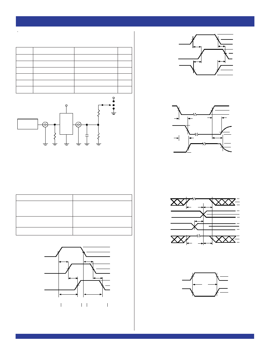
TEST CIRCUITS AND WAVEFORMS
Propagation Delay
Test Circuit for All Outputs
Set-up, Hold, and Release Times
NOTES:
1. For t
SK
(o) OUTPUT1 and OUTPUT2 are any two outputs.
2. For t
SK
(b) OUTPUT1 and OUTPUT2 are in the same bank.
DEFINITIONS:
C
L
= Load capacitance: includes jig and probe capacitance.
R
T
= Termination resistance: should be equal to Z
OUT
of the Pulse Generator.
NOTES:
1. Pulse Generator for All Pulses: Rate
10MHz; t
F
2ns; t
R
2ns.
2. Pulse Generator for All Pulses: Rate
10MHz; t
F
2.5ns; t
R
2.5ns.
Output Skew - t
SK
(
X
)
Pulse Width
Symbol
V
CC(1)
= 2.5V±0.2V
V
CC(2)
= 3.3V±0.3V & 2.7V
Unit
V
LOAD
2 x Vcc
6
V
V
IH
Vcc
2.7
V
V
T
Vcc
/ 2
1.5
V
V
LZ
150
300
mV
V
HZ
150
300
mV
C
L
30
50
pF
TEST CONDITIONS
SWITCH POSITION
Test
Switch
Open Drain
Disable Low
V
LOAD
Enable Low
Disable High
GND
Enable High
All Other Tests
Open
NOTE:
1. Diagram shown for input Control Enable-LOW and input Control Disable-HIGH.
Enable and Disable Times