74LVCH16701A.pmd
INDUSTRIAL TEMPERATURE RANGE
IDT74LVCH16701A
3.3V CMOS 18-BIT READ/WRITE BUFFER WITH 5V TOLERANT I/O
1
B
1-18
FF
CLK
RESET
OEAB
WCE
RCE
FIFO
(4 deep)
18
OEBA
LE
LATCH
A
1-18
18
29
55
2
56
30
27
28
LE
D
Q
1
3
54
OCTOBER 1999
INDUSTRIAL TEMPERATURE RANGE
The IDT logo is a registered trademark of Integrated Device Technology, Inc.
© 1999 Integrated Device Technology, Inc.
DSC-4233/3
FEATURES:
· Typical t
SK(o)
(Output Skew) < 250ps
· ESD > 2000V per MIL-STD-883, Method 3015; > 200V using
machine model (C = 200pF, R = 0)
· V
CC
= 3.3V ± 0.3V, Normal Range
· V
CC
= 2.7V to 3.6V, Extended Range
· CMOS power levels (0.4
µµ
µµ
µ W typ. static)
· All inputs, outputs, and I/O are 5V tolerant
· Supports hot insertion
· Available in SSOP, TSSOP, and TVSOP packages
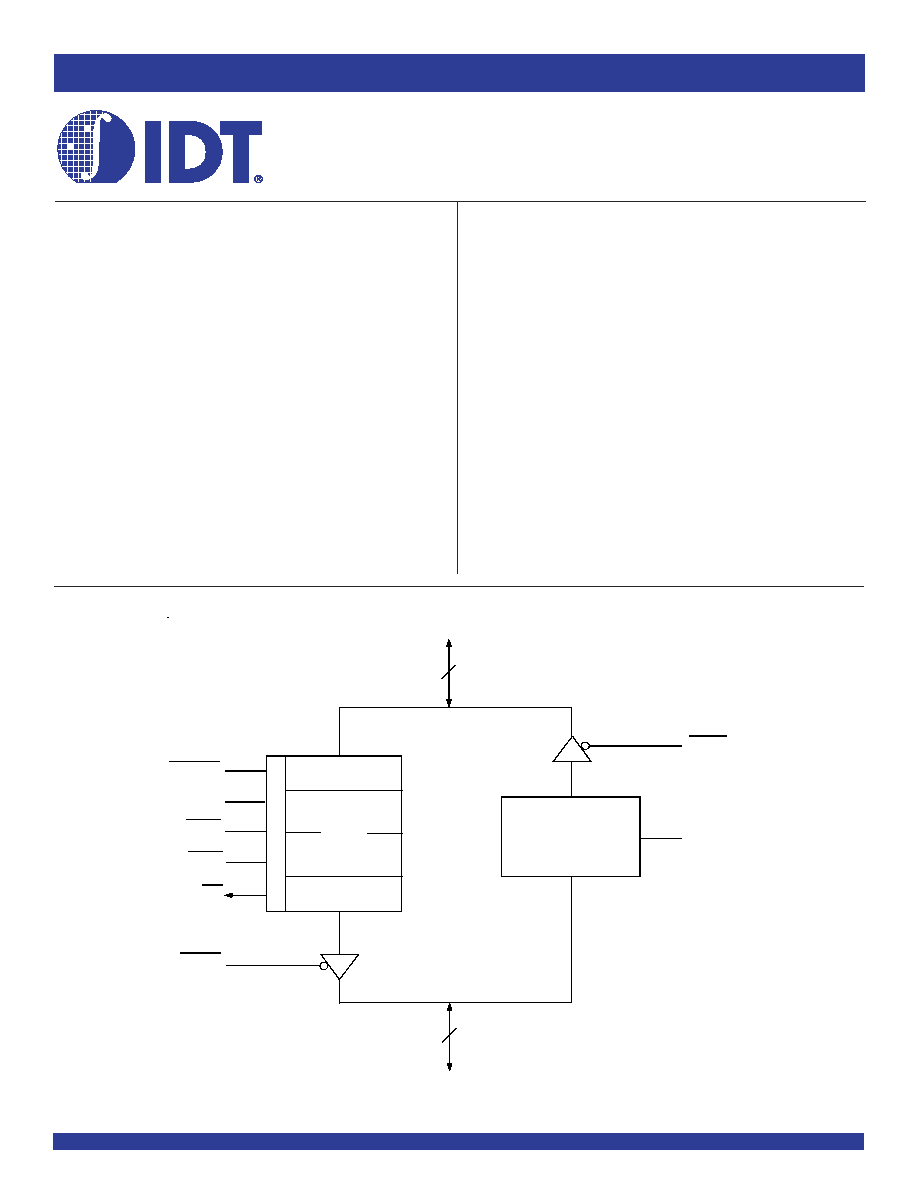
FUNCTIONAL BLOCK DIAGRAM
DRIVE FEATURES:
· High Output Drivers: ±24mA
· Reduced system switching noise
APPLICATIONS:
· 5V and 3.3V mixed voltage systems
· Data communication and telecommunication systems
IDT74LVCH16701A
DESCRIPTION:
The LVCH16701A 18-bit read/write buffer is built using advanced dual
metal CMOS technology. The device is designed as an 18-bit read/write
buffer with a four deep FIFO and a read-back latch. It can be used as a read/
write buffer between a CPU and a memory or to interface a high-speed bus
and a slow peripheral. The A-to-B (write) path has a four deep FIFO for
pipelined operations. The FIFO can be reset and a FIFO full condition is
indicated by the full flag (FF). The B-to-A (read) path has a latch.
All pins can be driven from either 3.3V or 5V devices. This feature allows
the use of this device as a translator in a mixed 3.3V/5V supply system.
The LVCH16701A has been designed with a ±24mA output driver. This
driver is capable of driving a moderate to heavy load while maintaining
speed performance.
The LVCH16701A has "bus-hold" which retains the inputs' last state
whenever the input goes to a high impedance. This prevents floating inputs
and eliminates the need for pull-up/down resistors.
3.3V CMOS
18-BIT READ/WRITE BUFFER
WITH 5 VOLT TOLERANT I/O
AND BUS-HOLD
INDUSTRIAL TEMPERATURE RANGE
2
IDT74LVCH16701A
3.3V CMOS 18-BIT READ/WRITE BUFFER WITH 5V TOLERANT I/O
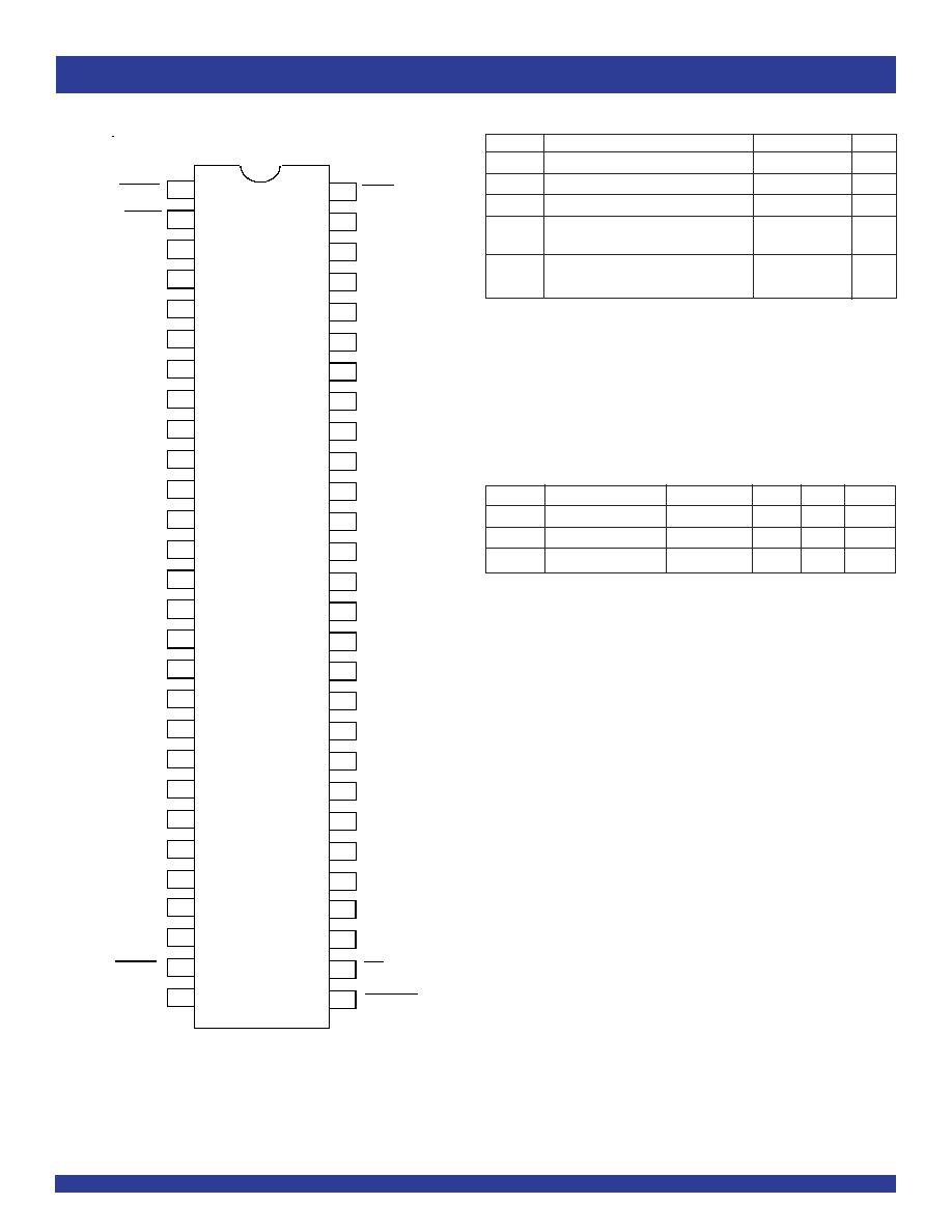
SSOP/ TSSOP/ TVSOP
TOP VIEW
PIN CONFIGURATION
Symbol
Description
Max
Unit
V
TERM
Terminal Voltage with Respect to GND
0.5 to +6.5
V
T
STG
Storage Temperature
65 to +150
°C
I
OUT
DC Output Current
50 to +50
mA
I
IK
Continuous Clamp Current,
50
mA
I
OK
V
I
< 0 or V
O
< 0
I
CC
Continuous Current through each
±100
mA
I
SS
V
CC
or GND
ABSOLUTE MAXIMUM RATINGS
(1)
NOTE:
1. Stresses greater than those listed under ABSOLUTE MAXIMUM RATINGS may cause
permanent damage to the device. This is a stress rating only and functional operation
of the device at these or any other conditions above those indicated in the operational
sections of this specification is not implied. Exposure to absolute maximum rating
conditions for extended periods may affect reliability.
NOTE:
1. As applicable to the device type.
Symbol
Parameter
(1)
Conditions
Typ.
Max.
Unit
C
IN
Input Capacitance
V
IN
= 0V
4.5
6
pF
C
OUT
Output Capacitance
V
OUT
= 0V
6.5
8
pF
C
I/O
I/O Port Capacitance
V
IN
= 0V
6.5
8
pF
CAPACITANCE
(T
A
= +25°C, F = 1.0MHz)
OEAB
GND
V
CC
A
4
GND
GND
V
CC
A
15
LE
2
3
4
5
6
7
8
9
10
11
12
13
14
15
16
17
18
19
20
21
22
23
24
47
46
45
44
43
42
41
40
39
38
37
36
35
34
33
48
49
50
51
52
53
54
55
56
1
GND
V
CC
GND
GND
V
CC
GND
GND
25
26
27
28
32
31
30
29
RESET
WCE
A
1
A
2
A
3
A
5
A
6
A
7
A
8
A
9
A
10
A
11
A
12
A
13
A
14
A
16
A
17
A
18
OEBA
RCE
CLK
B
1
B
2
B
3
B
4
B
5
B
6
B
7
B
8
B
10
B
11
B
12
B
9
B
13
B
14
B
15
B
16
B
17
B
18
FF
INDUSTRIAL TEMPERATURE RANGE
IDT74LVCH16701A
3.3V CMOS 18-BIT READ/WRITE BUFFER WITH 5V TOLERANT I/O
3
NOTE:
1. These pins have "Bus-Hold". All other pins are standard inputs, outputs, or I/Os.
FUNCTIONAL DESCRIPTION
This device is useful as a read/write buffer for modular high end designs.
It provides multi-level buffering in the write path and single deep buffering
in the read path, and is suited to write back cache implementation. The read
path provides a transparent latch.
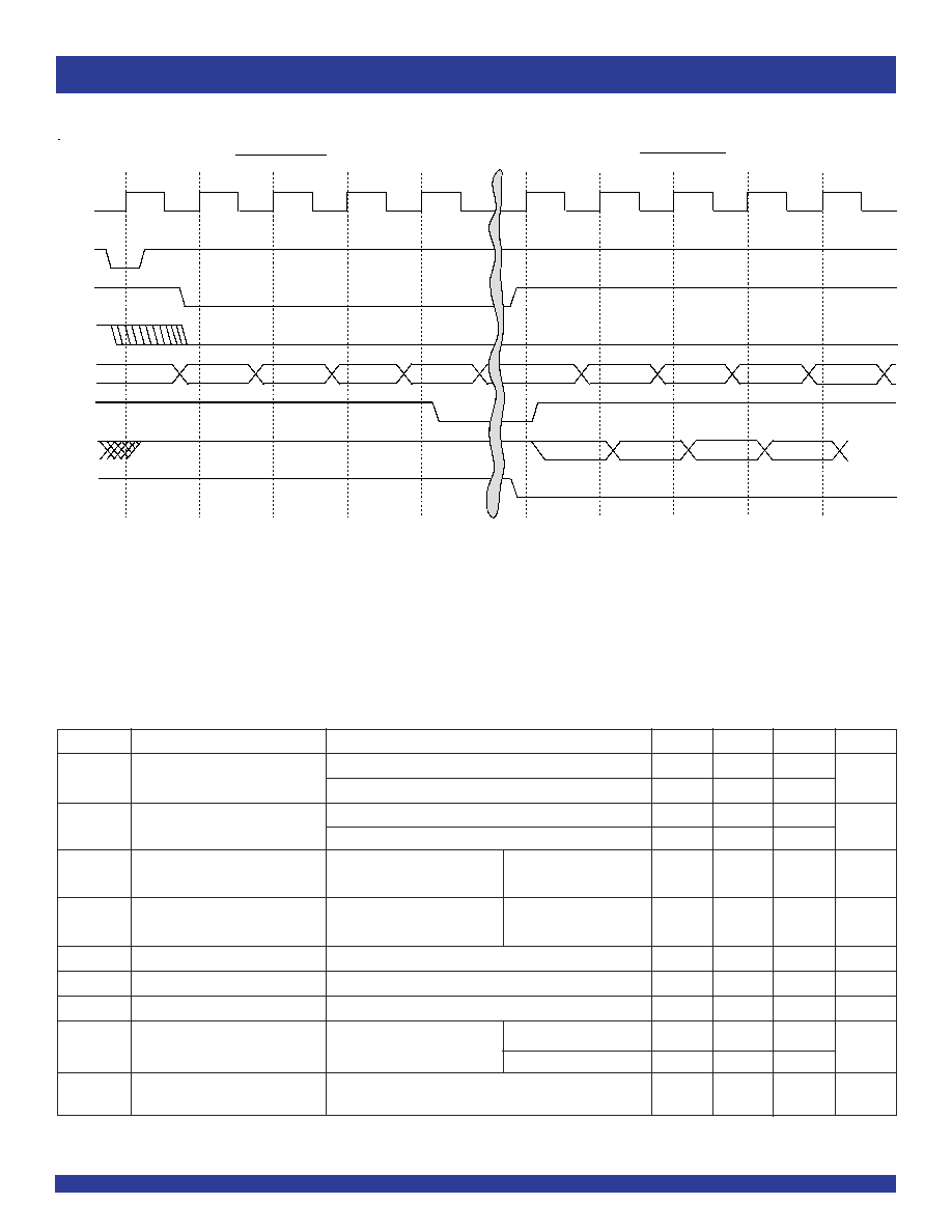
The four deep FIFO uses one clock with two clock enable pins, WCE and
RCE to clock data in and out. The FIFO has an external full flag which goes
LOW when the FIFO is full. Internal read and write pointers keep track of
the words stored in the FIFO. A write attempt to a full FIFO is ignored. An
attempt to read from an empty FIFO will have no effect and the last read data
remains at the output of the FIFO. The FIFO may be reset by the
synchronous RESET input. This resets the read and write pointers to the
original "empty" condition and also sets all B outputs = 1. Simultaneous read
and write attempts (clock data into FIFO as well as clock data out of FIFO)
are possible except on FIFO empty and full boundaries. When the FIFO
is empty, and a simultaneous read and write is attempted, the read is ignored
while the write is executed. If the same is attempted when the FIFO is full,
the write is ignored while the read is executed. Normal operation of the four
deep FIFO in the write path is independent of the read path operation.
Pin Names
I/O
Description
A
1-18
I/O
18 bit I/O port
(1)
B
1-18
I/O
18 bit I/O port
(1)
CLK
I
Clock for write path FIFO. Clocks data into FIFO when WCE is low, clocks data out of FIFO when RCE is low. When FIFO is full all further
writes to the FIFO are inhibited. When FIFO is empty all reads from the
FIFO are inhibited. CLK also resets the FIFO when RESET is low.
WCE
I
Enable pin for FIFO input clock (Active LOW)
RCE
I
Enable pin for FIFO output clock (Active LOW)
FF
O
Write path FIFO full flag. Goes low when FIFO is full.
RESET
I
Synchronous FIFO reset - when low CLK resets the FIFO. The FIFO pointers are initialized to the "empty" condition and FIFO output is forced
high (all ones). The FIFO full flag (FF) will be high immediately after reset. (Active LOW)
OEAB
I
Output Enable pin for B port (Active LOW)
OEBA
I
Output Enable pin for A port (Active LOW)
LE
I
Read path latch enable pin. When high, data flows transparently from B port to A port, B data is latched on the falling edge of LE. (Note: LE is independent
of CLK and data)
PIN DESCRIPTION
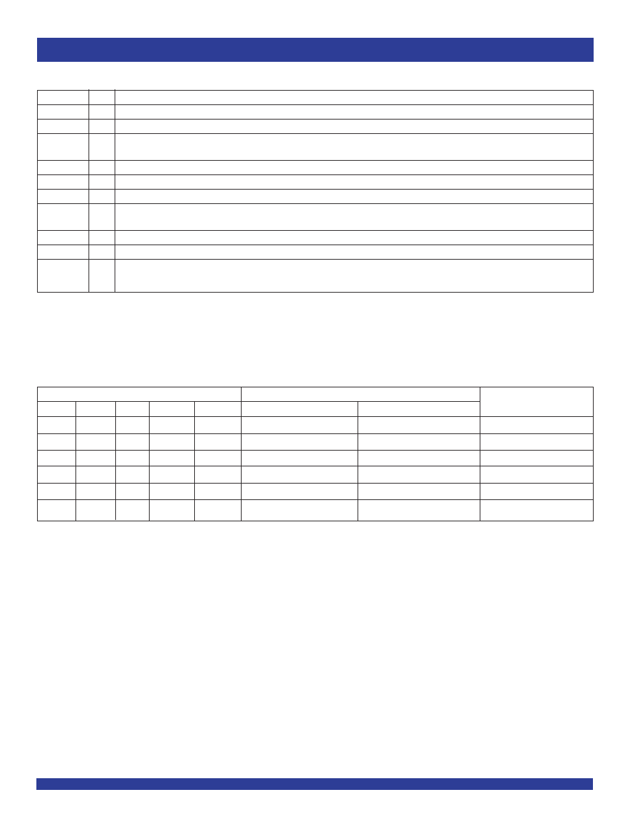
FUNCTION TABLE
(1)
Inputs
Outputs
OEBA
OEAB
LE
RESET
CLK
Ax
Bx
Notes
H
H
H
H
Q
(2)
(B) Bus Hold
Q
(2)
(A) -4CLKS Bus Hold
L
H
H
H
B to A
Transparent Mode
L
H
L
H
Qo(B)
H
H
X
H
Q
(2)
(A) Bus Hold
Q
(2)
(B) Bus Hold
H
L
X
H
A to B - 4 CLKS
L
L
L
H
Q
(2)
(B) Bus Hold
Q
(2)
(B) - 4 CLKS Bus Hold
Case not recommended
NOTES:
1. H = HIGH Voltage Level
L = LOW Voltage Level
X = Don't Care
= LOW-to-HIGH Transition
2. Level of Q before the indicated steady-state input conditions were established.
INDUSTRIAL TEMPERATURE RANGE
4
IDT74LVCH16701A
3.3V CMOS 18-BIT READ/WRITE BUFFER WITH 5V TOLERANT I/O
Symbol
Parameter
Test Conditions
Min.
Typ.
(1)
Max.
Unit
V
IH
Input HIGH Voltage Level
V
CC
= 2.3V to 2.7V
1.7
--
--
V
V
CC
= 2.7V to 3.6V
2
--
--
V
IL
Input LOW Voltage Level
V
CC
= 2.3V to 2.7V
--
--
0.7
V
V
CC
= 2.7V to 3.6V
--
--
0.8
I
IH
Input Leakage Current
V
CC
= 3.6V
V
I
= 0 to 5.5V
--
--
±5
µA
I
IL
I
OZH
High Impedance Output Current
V
CC
= 3.6V
V
O
= 0 to 5.5V
--
--
±10
µA
I
OZL
(3-State Output pins)
I
OFF
Input/Output Power Off Leakage
V
CC
= 0V, V
IN
or V
O
5.5V
--
--
±50
µA
V
IK
Clamp Diode Voltage
V
CC
= 2.3V, I
IN
= 18mA
--
0.7
1.2
V
V
H
Input Hysteresis
V
CC
= 3.3V
--
100
--
mV
I
CCL
Quiescent Power Supply Current
V
CC
= 3.6V
V
IN
= GND or V
CC
--
--
10
µA
I
CCH
I
CCZ
3.6
V
IN
5.5V
(2)
--
--
10
I
CC
Quiescent Power Supply Current
One input at V
CC
- 0.6V, other inputs at V
CC
or GND
--
--
500
µA
Variation
DC ELECTRICAL CHARACTERISTICS OVER OPERATING RANGE
Following Conditions Apply Unless Otherwise Specified:
Operating Condition: T
A
= 40°C to +85°C
NOTES:
1. Typical values are at V
CC
= 3.3V, +25°C ambient.
2. This applies in the disabled state only.
TIMING DIAGRAM
CLK
RESET
WCE
OEAB
FF
RCE
WORD 1
WORD 2
WORD 3
WORD 4
WORD 1
WORD 2
WORD 3
WORD 4
WRITE CYCLES
Cycle 1
Cycle 2
Cycle 3
Cycle 4
Cycle 1
Cycle 2
Cycle 3
Cycle 4
READ CYCLES
B [1:18]
A [1:18]
INDUSTRIAL TEMPERATURE RANGE
IDT74LVCH16701A
3.3V CMOS 18-BIT READ/WRITE BUFFER WITH 5V TOLERANT I/O
5
NOTE:
1. V
IH
and V
IL
must be within the min. or max. range shown in the DC ELECTRICAL CHARACTERISTICS OVER OPERATING RANGE table for the appropriate V
CC
range.
T
A
= 40°C to + 85°C.
OUTPUT DRIVE CHARACTERISTICS
Symbol
Parameter
Test Conditions
(1)
Min.
Max.
Unit
V
OH
Output HIGH Voltage
V
CC
= 2.3V to 3.6V
I
OH
= 0.1mA
V
CC
0.2
--
V
V
CC
= 2.3V
I
OH
= 6mA
2
--
V
CC
= 2.3V
I
OH
= 12mA
1.7
--
V
CC
= 2.7V
2.2
--
V
CC
= 3V
2.4
--
V
CC
= 3V
I
OH
= 24mA
2
--
V
OL
Output LOW Voltage
V
CC
= 2.3V to 3.6V
I
OL
= 0.1mA
--
0.2
V
V
CC
= 2.3V
I
OL
= 6mA
--
0.4
I
OL
= 12mA
--
0.7
V
CC
= 2.7V
I
OL
= 12mA
--
0.4
V
CC
= 3V
I
OL
= 24mA
--
0.55
OPERATING CHARACTERISTICS, V
CC
= 3.3V ± 0.3V, T
A
= 25°C
Symbol
Parameter
Test Conditions
Typical
Unit
C
PD
Power Dissipation WCE Mode, OEAB = 0
C
L
= 0pF, f = 10Mhz
pF
C
PD
Power Dissipation RCE Mode, OEBA = 0
C
PD
Registered Channel (B to A)
Power Dissipation OEBA = 0; CE = 0
C
PD
Registered Channel
Power Dissipation OEBA = 0; CE = 1
BUS-HOLD CHARACTERISTICS
Symbol
Parameter
(1)
Test Conditions
Min.
Typ.
(2)
Max.
Unit
I
BHH
Bus-Hold Input Sustain Current
V
CC
= 3V
V
I
= 2V
75
--
--
µA
I
BHL
V
I
= 0.8V
75
--
--
I
BHH
Bus-Hold Input Sustain Current
V
CC
= 2.3V
V
I
= 1.7V
--
--
--
µA
I
BHL
V
I
= 0.7V
--
--
--
I
BHHO
Bus-Hold Input Overdrive Current
V
CC
= 3.6V
V
I
= 0 to 3.6V
--
--
±500
µA
I
BHLO
NOTES:
1. Pins with Bus-Hold are identified in the pin description.
2. Typical values are at V
CC
= 3.3V, +25°C ambient.