74LVCHR16543A.pmd
INDUSTRIAL TEMPERATURE RANGE
IDT74LVCHR16543A
3.3V CMOS 16-BIT REGISTERED TRANSCEIVER WITH 3-STATE OUTPUTS
1
OCTOBER 1999
INDUSTRIAL TEMPERATURE RANGE
The IDT logo is a registered trademark of Integrated Device Technology, Inc.
© 1999 Integrated Device Technology, Inc.
DSC-4680/1
FEATURES:
· Typical t
SK(o)
(Output Skew) < 250ps
· ESD > 2000V per MIL-STD-883, Method 3015; > 200V using
machine model (C = 200pF, R = 0)
· V
CC
= 3.3V ± 0.3V, Normal Range
· V
CC
= 2.7V to 3.6V, Extended Range
· CMOS power levels (0.4
µµ
µµ
µ W typ. static)
· All inputs, outputs, and I/O are 5V tolerant
· Supports hot insertion
· Available in SSOP, TSSOP, and TVSOP packages
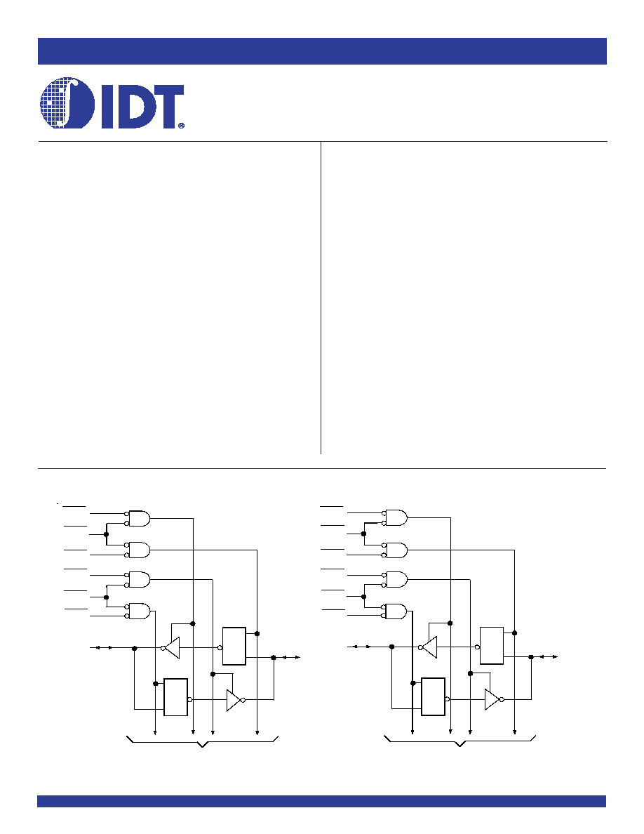
FUNCTIONAL BLOCK DIAGRAM
DRIVE FEATURES:
· Balanced Output Drivers: ±12mA
· Low switching noise
APPLICATIONS:
· 5V and 3.3V mixed voltage systems
· Data communication and telecommunication systems
IDT74LVCHR16543A
3.3V CMOS 16-BIT
REGISTERED TRANSCEIVER
WITH 3-STATE OUTPUTS,
5 VOLT TOLERANT I/O, BUS-HOLD
C1
1D
1
B
1
1
LEAB
1
CEAB
1
OEAB
1
LEBA
1
CEBA
1
OEBA
TO SEVEN OTHER CHANNELS
1
A
1
2
B
1
2
LEAB
2
CEAB
2
OEAB
2
LEBA
2
CEBA
2
OEBA
2
A
1
56
54
55
1
3
2
5
29
31
30
28
26
27
15
42
52
C1
1D
C1
1D
C1
1D
TO SEVEN OTHER CHANNELS
DESCRIPTION:
The LVCHR16543A 16-bit registered transceiver is built using advanced
dual metal CMOS technology. The LVCHR16543A device can be used as
two independent 8-bit transceivers or one 16-bit transceiver. Separate
latch-enable (LEAB or LEBA) and output-enable(OEAB or OEBA) inputs
are provided for each register to permit independent control in either
direction of data flow. The A-to-B enable (CEAB) must be low in order to enter
data from A or to output data from B. If CEAB is low and LEAB is low, the A-
to-B latches are transparent; a subsequent low-to-high transition of LEAB
puts the A latches in the storage mode. With CEAB and OEAB both low, the
3-state B outputs are active and reflect the data present at the output of the
A latches. Data flow from B to A is similar, but requires using the CEBA, LEBA,
and OEBA inputs. To ensure the high-impedance state during power up or
power down, OE should be tied to Vcc through a pullup resistor; the minmum
value of the resistor is determined by the current sinking capability of the
driver.
The LVCHR16543A has series resistors in the device output structure
which will significantly reduce line noise when used with light loads. The
driver has been designed to drive ±12mA at the designated threshold levels.
Inputs can be driven from either 3.3V or 5V devices. This feature allows
the use of this device as a translator in a mixed 3.3V/5V supply system.
The LVCHR16543A has "bus-hold" which retains the input's last state
whenever the input goes to a high impedance. This prevents floating inputs
and eliminates the need for pull-up/down resistors.
INDUSTRIAL TEMPERATURE RANGE
2
IDT74LVCHR16543A
3.3V CMOS 16-BIT REGISTERED TRANSCEIVER WITH 3-STATE OUTPUTS
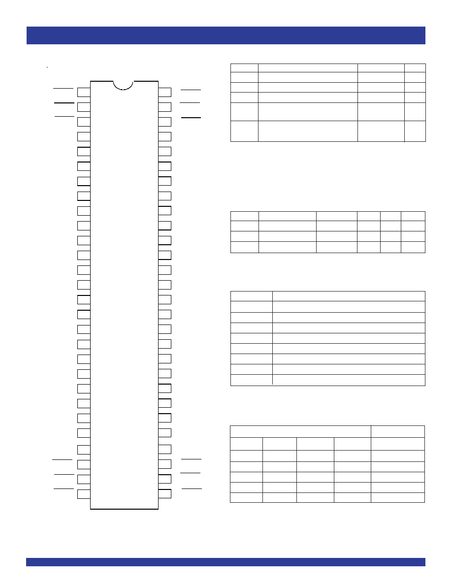
SSOP/ TSSOP/ TVSOP
TOP VIEW
PIN CONFIGURATION
Symbol
Description
Max
Unit
V
TERM
Terminal Voltage with Respect to GND
0.5 to +6.5
V
T
STG
Storage Temperature
65 to +150
°C
I
OUT
DC Output Current
50 to +50
mA
I
IK
Continuous Clamp Current,
50
mA
I
OK
V
I
< 0 or V
O
< 0
I
CC
Continuous Current through each
±100
mA
I
SS
V
CC
or GND
ABSOLUTE MAXIMUM RATINGS
(1)
NOTE:
1. Stresses greater than those listed under ABSOLUTE MAXIMUM RATINGS may cause
permanent damage to the device. This is a stress rating only and functional operation
of the device at these or any other conditions above those indicated in the operational
sections of this specification is not implied. Exposure to absolute maximum rating
conditions for extended periods may affect reliability.
1
OEAB
GND
1
A
1
1
A
2
V
CC
1
A
3
1
A
4
GND
1
A
5
1
A
6
GND
V
CC
2
3
4
5
6
7
8
9
10
11
12
13
14
15
16
17
18
19
20
21
22
23
24
47
46
45
44
43
42
41
40
39
38
37
36
35
34
33
48
49
50
51
52
53
54
55
56
1
GND
2
CEAB
25
26
27
28
32
31
30
29
1
LEAB
1
CEAB
1
A
7
1
A
8
2
A
1
2
A
2
2
A
3
2
A
4
2
A
5
2
A
6
2
A
7
2
A
8
2
LEAB
2
OEAB
1
OEBA
GND
1
B
1
1
B
2
V
CC
1
B
3
1
B
4
GND
1
B
5
1
B
6
GND
V
CC
GND
2
CEBA
1
LEBA
1
CEBA
1
B
7
1
B
8
2
B
1
2
B
2
2
B
3
2
B
4
2
B
5
2
B
6
2
B
7
2
B
8
2
LEBA
2
OEBA
NOTE:
1. As applicable to the device type.
Symbol
Parameter
(1)
Conditions
Typ.
Max.
Unit
C
IN
Input Capacitance
V
IN
= 0V
4.5
6
pF
C
OUT
Output Capacitance
V
OUT
= 0V
6.5
8
pF
C
I/O
I/O Port Capacitance
V
IN
= 0V
6.5
8
pF
CAPACITANCE
(T
A
= +25°C, F = 1.0MHz)
NOTES:
1. H = HIGH Voltage Level
L = LOW Voltage Level
X = Don't Care
Z = High-Impedance
2. A-to-B data flow is shown. B-to-A data flow is similar but uses CEBA, LEBA, and OEBA.
3. Before LEAB LOW-to-HIGH transition.
Inputs
Output Buffers
xCEAB
xLEAB
xOEAB
xAx
xBx
H
X
X
X
Z
X
X
H
X
Z
L
H
L
X
B
(3)
L
L
L
L
L
L
L
L
H
H
FUNCTION TABLE
(EACH 8-BIT SECTION)
(1,2)
NOTE:
1. These pins have "Bus-Hold". All other pins are standard inputs, outputs, or I/Os.
Pin Names
Description
xOEAB
A-to-B Output Enable Input (Active LOW)
xOEBA
B-to-A Output Enable Input (Active LOW)
xCEAB
A-to-B Enable Input (Active LOW)
xCEBA
B-to-A Enable Input (Active LOW)
xLEAB
A-to-B Latch Enable Input (Active LOW)
xLEBA
B-to-A Latch Enable Input (Active LOW)
xAx
A-to-B Data Inputs or B-to-A 3-State Outputs
(1)
xBx
B-to-A Data Inputs or A-to-B 3-State Outputs
(1)
PIN DESCRIPTION
INDUSTRIAL TEMPERATURE RANGE
IDT74LVCHR16543A
3.3V CMOS 16-BIT REGISTERED TRANSCEIVER WITH 3-STATE OUTPUTS
3
Symbol
Parameter
Test Conditions
Min.
Typ.
(1)
Max.
Unit
V
IH
Input HIGH Voltage Level
V
CC
= 2.3V to 2.7V
1.7
--
--
V
V
CC
= 2.7V to 3.6V
2
--
--
V
IL
Input LOW Voltage Level
V
CC
= 2.3V to 2.7V
--
--
0.7
V
V
CC
= 2.7V to 3.6V
--
--
0.8
I
IH
Input Leakage Current
V
CC
= 3.6V
V
I
= 0 to 5.5V
--
--
±5
µA
I
IL
I
OZH
High Impedance Output Current
V
CC
= 3.6V
V
O
= 0 to 5.5V
--
--
±10
µA
I
OZL
(3-State Output pins)
I
OFF
Input/Output Power Off Leakage
V
CC
= 0V, V
IN
or V
O
5.5V
--
--
±50
µA
V
IK
Clamp Diode Voltage
V
CC
= 2.3V, I
IN
= 18mA
--
0.7
1.2
V
V
H
Input Hysteresis
V
CC
= 3.3V
--
100
--
mV
I
CCL
Quiescent Power Supply Current
V
CC
= 3.6V
V
IN
= GND or V
CC
--
--
10
µA
I
CCH
I
CCZ
3.6
V
IN
5.5V
(2)
--
--
10
I
CC
Quiescent Power Supply Current
One input at V
CC
- 0.6V, other inputs at V
CC
or GND
--
--
500
µA
Variation
DC ELECTRICAL CHARACTERISTICS OVER OPERATING RANGE
Following Conditions Apply Unless Otherwise Specified:
Operating Condition: T
A
= 40°C to +85°C
NOTES:
1. Typical values are at V
CC
= 3.3V, +25°C ambient.
2. This applies in the disabled state only.
BUS-HOLD CHARACTERISTICS
Symbol
Parameter
(1)
Test Conditions
Min.
Typ.
(2)
Max.
Unit
I
BHH
Bus-Hold Input Sustain Current
V
CC
= 3V
V
I
= 2V
75
--
--
µA
I
BHL
V
I
= 0.8V
75
--
--
I
BHH
Bus-Hold Input Sustain Current
V
CC
= 2.3V
V
I
= 1.7V
--
--
--
µA
I
BHL
V
I
= 0.7V
--
--
--
I
BHHO
Bus-Hold Input Overdrive Current
V
CC
= 3.6V
V
I
= 0 to 3.6V
--
--
±500
µA
I
BHLO
NOTES:
1. Pins with Bus-Hold are identified in the pin description.
2. Typical values are at V
CC
= 3.3V, +25°C ambient.
INDUSTRIAL TEMPERATURE RANGE
4
IDT74LVCHR16543A
3.3V CMOS 16-BIT REGISTERED TRANSCEIVER WITH 3-STATE OUTPUTS
NOTE:
1. V
IH
and V
IL
must be within the min. or max. range shown in the DC ELECTRICAL CHARACTERISTICS OVER OPERATING RANGE table for the appropriate V
CC
range.
T
A
= 40°C to + 85°C.
OUTPUT DRIVE CHARACTERISTICS
Symbol
Parameter
Test Conditions
(1)
Min.
Max.
Unit
V
OH
Output HIGH Voltage
V
CC
= 2.3V to 3.6V
I
OH
= 0.1mA
V
CC
0.2
--
V
V
CC
= 2.3V
I
OH
= 4mA
1.9
--
I
OH
= 6mA
1.7
--
V
CC
= 2.7V
I
OH
= 4mA
2.2
--
I
OH
= 8mA
2
--
V
CC
= 3V
I
OH
= 6mA
2.4
--
I
OH
= 12mA
2
--
V
OL
Output LOW Voltage
V
CC
= 2.3V to 3.6V
I
OL
= 0.1mA
--
0.2
V
V
CC
= 2.3V
I
OL
= 4mA
--
0.4
I
OL
= 6mA
--
0.55
V
CC
= 2.7V
I
OL
= 4mA
--
0.4
I
OL
= 8mA
--
0.6
V
CC
= 3V
I
OL
= 6mA
--
0.55
I
OL
= 12mA
--
0.8
OPERATING CHARACTERISTICS, V
CC
= 3.3V ± 0.3V, T
A
= 25°C
Symbol
Parameter
Test Conditions
Typical
Unit
C
PD
Power Dissipation Capacitance per Transceiver Outputs enabled
C
L
= 0pF, f = 10Mhz
pF
C
PD
Power Dissipation Capacitance per Transceiver Outputs disabled
INDUSTRIAL TEMPERATURE RANGE
IDT74LVCHR16543A
3.3V CMOS 16-BIT REGISTERED TRANSCEIVER WITH 3-STATE OUTPUTS
5
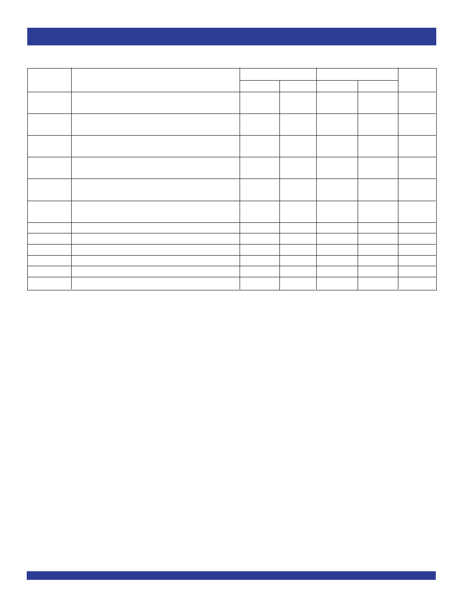
SWITCHING CHARACTERISTICS
(1)
V
CC
= 2.7V
V
CC
= 3.3V ± 0.3V
Symbol
Parameter
Min.
Max.
Min.
Max.
Unit
t
PLH
Propagation Delay
1.5
7
1.5
6
ns
t
PHL
xAx to xBx or xBx to xAx
t
PLH
Propagation Delay
1.5
8
1.5
7
ns
t
PHL
xLEBA to xAx, xLEAB to xBx
t
PZH
Output Enable Time
1.5
9
1.5
8
ns
t
PZL
xCEBA or xCEAB to xAx or xBx
t
PZH
Output Enable Time
1.5
9
1.5
8
ns
t
PZL
xOEBA or xOEAB to xAx or xBx
t
PHZ
Output Disable Time
1.5
7.5
1.5
6.5
ns
t
PLZ
xCEBA or xCEAB to xAx or xBx
t
PHZ
Output Disable Time
1.5
7.5
1.5
6.5
ns
t
PLZ
xOEBA or xOEAB to xAx or xBx
t
SU
Set-up Time, data before CE
2
--
2
--
ns
t
SU
Set-up Time, data before LE
, CE LOW
2
--
2
--
ns
t
H
Hold Time, data after CE
2
--
2
--
ns
t
H
Hold Time, data after LE
, CE LOW
2
--
2
--
ns
t
W
Pulse Duration, xLEBA or xLEAB, xCEBA or xCEAB LOW
5
--
5
--
ns
t
SK
(o)
Output Skew
(2)
--
--
--
500
ps
NOTES:
1. See TEST CIRCUITS AND WAVEFORMS. T
A
= 40°C to + 85°C.
2. Skew between any two outputs of the same package and switching in the same direction.