
1 of 21
June 24, 2002
2002 Integrated Device Technology, Inc.
DSC 4308/4
IDT and the IDT logo are registered trademarks of Integrated Device Technology, Inc.
Data Path Interface (DPI) to
Utopia Level 1
Translation Device
Features
Features
Features
Features
!
Single chip ATM Layer UTOPIA Level 1 to 4-bit DPI interface.
!
Supports ATM Forum UTOPIA Level 1 interface.
!
Supports ATM device interface in Cell mode.
!
Capable of full-duplex operation up-to 160 Mbps.
!
Utility bus interface to access PHY registers.
!
In-stream control to access PHY registers.
Description
Description
Description
Description
The 77010 interfaces a UTOPIA PHY device to a device that uses a
Data Path Interface (DPI). Examples of PHY devices may include the
IDT77105, and the IDT77V400 Switching Memory is an example of a
component that utilizes a DPI interface. Figure 1 illustrates a typical
application using the IDT77010.
The UTOPIA level 1 bus interface runs at speeds up to 155 Mbps,
with the DPI-4 interface capable of full duplex operation at 160 Mbps.
In-stream programming is used to read and write to the PHY regis-
ters, with the Control Cells being generated from a remote controlling
agent. The Control Cells are used to configure, control and retrieve
status of the PHY device.
Theory of Operation
Theory of Operation
Theory of Operation
Theory of Operation
UTOPIA receive cells are transferred to the DPI-4 interface one cell
at a time. The DPI-4 clock rate is twice the frequency of receive UTOPIA
clock.
DPI-4 transmit cells are transferred to the UTOPIA transmit bus one
cell at a time. Transmit flow control is used to match the transmit cell rate
to the PHY's transmit cell rate.
Control cells are inserted and decoded by the control cell decoder.
The control cells are filtered and will not be transferred to the UTOPIA
transmit bus.
The control cell decoder block identifies the control cells and signals
the Utility Bus Interface to execute the commands. For a Utility bus write
command cell, the Utility bus does a one byte write to the specified
Utility bus address. For a Utility bus read command cell, the Utility bus
reads one byte from the specified Utility bus address and loads this byte
to the Cell Generator logic. The Cell Generator makes a request to the
receive cell arbiter to process the cell, and generates a status cell if no
UTOPIA receive cell is detected.
A status cell is a complete ATM cell generated and loaded to the
Receive DPI-4 I/F logic.
A receive cell on the DPI-4 bus is either an ATM cell from the receive
UTOPIA bus or a status ATM cell locally generated. Internally generated
ATM cells are output to the Receive DPI-4 Interface only when there are
no UTOPIA Receive cell. Figure 2 below shows the device data flow.
Block Diagram
Block Diagram
Block Diagram
Block Diagram
Figure 1 Typical IDT77010 Application
OC-3
or
STS-3
OC-3
PHY
IDT77010
UTOPIA L1
to DPI I/F
Utility bus
Switching
Memory
IDT77V400
4308 drw 01
"
"
"
"
"
"
UTOPIA L1
Receive
UTOPIA L1
Transmit
DPI Receive
DPI Transmit
4
4
.
IDT77010

2 of 21
June 24, 2002
IDT77010
Block Diagram
Block Diagram
Block Diagram
Block Diagram
Figure 2 Functional Block Diagram
Pin Configuration
Pin Configuration
Pin Configuration
Pin Configuration
1,2
1,2
1,2
1,2
1.
All power pins must be connected to the appropriate power supply.
V
CC
pins to 5.0V � 0.25V; V
DD
pins to 3.3V � 0.3V.
2.
All GND pins must be connected to ground supply.
3.
This text does not indicate orientation of the actual part-marking.
Rx UTOPIA
Interface
Cell
MUX
Rx DPI-4
Interface
No Rx cell
detector/
arbiter
Cell
Generator
Tx UTOPIA
Interface
Control cell
filter
Tx DPI-4
Interface
Utility Bus
Interface
Control cell
Decoder
SysClk/2
SYSCLK
4308 drw 02
UTOPIA
Interface
DPI-4
Interface
8
8
8
4
4
INDEX
TSOC
T
X
DATA4
T
X
DATA2
T
X
DATA5
G
N
D
G
N
D
T
X
PRTY
T
X
DATA7
T
X
DATA6
GND
V
CC
T
X
DATA1
T
X
DATA0
GND
V
CC
TCLK
TCLAV
TENB
4308 drw 03
IDT77010
PQFP
TOP
VIEW
3
8
9
10
11
12
13
14
15
16
1
2
3
4
5
6
7
46
45
44
43
42
41
56
55
54
53
52
51
50
47
48
49
3
2
3
1
3
0
2
9
2
8
2
7
2
6
2
5
2
4
2
3
2
2
2
1
6
3
6
2
6
1
6
4
3
3
3
4
3
5
3
6
3
7
3
8
3
9
4
0
6
5
6
6
6
7
6
8
6
9
7
0
7
1
7
2
7
3
7
4
7
5
7
6
7
7
7
8
7
9
8
0
17
18
19
20
57
58
59
60
GND
GND
CONT_A
T
X
DATA3
V
DD
T
x
L
E
D
P
H
Y
C
S
P
H
Y
R
S
T
V
C
C
W
R
I
T
E
R
E
A
D
P
H
Y
I
N
T
V
C
C
G
N
D
V
D
D
ALE
RSOC
V
CC
GND
R
X
DATA
R
X
DATA
R
X
DATA
R
X
DATA
R
X
DATA
R
X
DATA
R
X
DATA
V
CC
GND
R
X
DATA
RCLK
RCLAV
RENB
RxLED
V
DD
V
D
D
C
O
N
T
_
B
R
S
T
L
C
R
S
T
S
Y
S
C
L
K
G
N
D
V
D
D
D
R
X
C
L
K
D
R
x
F
R
M
D
T
X
D
A
T
A
0
D
T
X
F
R
M
D
T
X
C
L
K
G
N
D
A
D
D
/
D
A
T
A
0
A
D
D
/
D
A
T
A
1
A
D
D
/
D
A
T
A
2
A
D
D
/
D
A
T
A
3
A
D
D
/
D
A
T
A
4
A
D
D
/
D
A
T
A
5
A
D
D
/
D
A
T
A
6
A
D
D
/
D
A
T
A
7
D
T
X
D
A
T
A
1
D
T
X
D
A
T
A
2
D
T
X
D
A
T
A
3
D
R
X
D
A
T
A
0
D
R
X
D
A
T
A
1
D
R
X
D
A
T
A
2
D
R
X
D
A
T
A
3

3 of 21
June 24, 2002
IDT77010
Pin Definitions
Pin Definitions
Pin Definitions
Pin Definitions
Signal Name
Pin
Number
Input/
Output
Description
SysClk
29
I
System Clock. All the device circuits are synchronized to this clock.
RST
23
I
System Reset. When low the 77010 and the PHY are reset. This is used as a global line card reset where all
the RST signals from all line cards are connected together.
LCRST
24
I
Line Card reset. When low the 77010 and the PHY are reset. This is a local line card reset used to reset a
specific 77010 and PHY on a specific line card.
CONT_A
19
O
Output Control Pin A. This pin is controlled by a receive control cell. Default output = low.
CONT_B
22
O
Output Control Pin B. This pin is controlled by a receive control cell. Default output = low.
RxLED
42
O
Active low. When low a receive cell is being transferred.
This pin may be used for receive activity LED.
TxLED
79
O
Active low. When low a transmit cell is being transferred.
This pin may be used for transmit activity LED.
READ
73
O
Utility bus read signal.
WRITE
74
O
Utility bus write signal.
ALE
59
O
Utility bus address latch enable. Used for latching the address on the address phase of the Add/Data bus.
Add/Data0
71
I/O
Utility bus multiplexed address and data bus.
Add/Data1
70
I/O
Utility bus multiplexed address and data bus.
Add/Data2
69
I/O
Utility bus multiplexed address and data bus.
Add/Data3
68
I/O
Utility bus multiplexed address and data bus.
Add/Data4
65
I/O
Utility bus multiplexed address and data bus.
Add/Data5
64
I/O
Utility bus multiplexed address and data bus.
Add/Data6
63
I/O
Utility bus multiplexed address and data bus.
Add/Data7
62
I/O
Utility bus multiplexed address and data bus.
PHYCS
78
O
Utility bus PHY chip select.
PHYINT
72
I
Utility bus PHY interrupt signal
PHYRST
77
O
Utility bus PHY reset.
RCLK
45
O
UTOPIA bus receive clock.
RSOC
58
I
UTOPIA bus receive start of cell.
RENB
43
O
UTOPIA bus receive enable.
RCLAV
44
I
UTOPIA bus receive cell available.
RxData0
46
I
UTOPIA bus receive data bit.
RxData1
49
I
UTOPIA bus receive data bit.
RxData2
50
I
UTOPIA bus receive data bit.
RxData3
51
I
UTOPIA bus receive data bit.
RxData4
52
I
UTOPIA bus receive data bit.
RxData5
53
I
UTOPIA bus receive data bit.
RxData6
54
I
UTOPIA bus receive data bit.

4 of 21
June 24, 2002
IDT77010
1.
All signals are 5.0V unless otherwise indicated.
2.
3.3V signals are 5.0V tolerant.
RxData7
55
I
UTOPIA bus receive data bit.
TENB
18
O
UTOPIA bus Transmit enable.
TCLK
16
O
UTOPIA bus transmit clock.
TCLAV
17
I
UTOPIA bus transmit cell available.
TSOC
2
O
UTOPIA bus transmit start of cell.
TxData0
13
O
UTOPIA bus transmit data bit.
TxData1
12
O
UTOPIA bus transmit data bit.
TxData2
11
O
UTOPIA bus transmit data bit.
TxData3
10
O
UTOPIA bus transmit data bit.
TxData4
9
O
UTOPIA bus transmit data bit.
TxData5
6
O
UTOPIA bus transmit data bit.
TxData6
5
O
UTOPIA bus transmit data bit.
TxData7
4
O
UTOPIA bus transmit data bit.
TxPrty
3
O
UTOPIA bus transmit data parity bit.
DTxClk
39
O
DPI-4 bus transmit clock. 3.3V Interface.
DTxFRM
38
I
DPI-4 bus transmit start of frame. 3.3V Interface.
DTxData0
37
I
DPI-4 bus transmit data bit. 3.3V Interface.
DTxData1
36
I
DPI-4 bus transmit data bit. 3.3V Interface.
DTxData2
35
I
DPI-4 bus transmit data bit. 3.3V Interface.
DTxData3
34
I
DPI-4 bus transmit data bit. 3.3V Interface.
DRxClk
32
O
DPI-4 bus receive clock. 3.3V Interface.
DRxFRM
33
O
DPI-4 bus receive start of frame. 3.3V Interface.
DRxData0
28
O
DPI-4 bus receive data bit. 3.3V Interface.
DRxData1
27
O
DPI-4 bus receive data bit. 3.3V Interface.
DRxData2
26
O
DPI-4 bus receive data bit. 3.3V Interface.
DRxData3
25
O
DPI-4 bus receive data bit. 3.3V Interface.
V
CC
8,15,48,57,67,76
Power
5.0V Power Supply Pins.
V
DD
1,21,31,41,61
Power
3.3V Power Supply Pins for DPI Interface.
GND
7,14,20,30,40,47
,56,60,66,75,80
GND
Ground Pins.
Signal Name
Pin
Number
Input/
Output
Description

5 of 21
June 24, 2002
IDT77010
Absolute Maximum Ratings
Absolute Maximum Ratings
Absolute Maximum Ratings
Absolute Maximum Ratings
Recommended Operating Conditions
Recommended Operating Conditions
Recommended Operating Conditions
Recommended Operating Conditions
DC Electrical Characteristics
DC Electrical Characteristics
DC Electrical Characteristics
DC Electrical Characteristics
Capacitance
Capacitance
Capacitance
Capacitance
Symbol
Parameter
Min
Max
Unit
V
CC
5V Digital Supply Voltage
-0.3
6.0
V
V
DD
3.3V Digital Supply Voltage
-0.3
4.6
V
V
IN
Digital Input Voltage
V
SS
V
CC
+ 0.5
V
I
OUT
Output Current
____
50
mA
T
STG
Storage Temperature
-55
140
�C
Symbol
Parameter
Min
Max
Unit
V
CC
5V Digital Supply Voltage
4.75
5.25
V
V
DD
3.3V Digital Supply Voltage
3.0
3.6
V
V
IN
TTL Input Voltage
-0.3
VCC+0.3
V
T
A
Operating Temperature
0
70
�C
titr
Input TTL rise time
____
2
ns
titf
Input TTL fall time
____
2
ns
V
IH
TTL Input High Voltage
2.0
____
V
V
IL
TTL Input Low Voltage
____
0.8
V
Symbol
Parameter
Test Conditions
77010
Unit
Min
Max
[I
LI
]
Input Leakage Current
V
CC
= 5.5V, VIN = 0V to VCC
10
10
� A
[I
LO
]
Output Leakage Current
V
OUT
= 0V to VCC
10
10
� A
V
OH
TTL Output High Voltage
I
OH
= -4mA
2.4
___
V
V
OL
TTL Output Low Voltage
I
OL
= +4mA
___
0.4
V
I
DD
Power Supply Current
155.52 Mbps
___
60
mA
I
CC
Power Supply Current
155.52 Mbps
___
12
mA
Symbol
Parameter
Test Conditions
Min
Type
Max
Unit
C
IN
Input Capacitance
All Inputs
___
4
___
pF
C
OUT
Output Capacitance
All Outputs
___
6
___
pF
C
BID
Bi-Directional Capacitance
All Bi-directional Pins
___
10
___
pF

6 of 21
June 24, 2002
IDT77010
Device Interface
Device Interface
Device Interface
Device Interface
This 77010 uses a UTOPIA level 1 interface to receive and transmit ATM cells to and from the PHY device. It mirrors the ATM layer as shown in
Figure 3 below.
Figure 3 DPI-4 to UTOPIA 1 Interface Device
DRxFRM
DRxCLK
DRxDATA[3:0]
DTxFRM
DTxCLK
DTxDATA[3:0]
RSOC
RCLK
RxDATA[7:0]
RENB
RCLAV
TSOC
TCLK
TxDATA[7:0]
TENB
TCLAV
PHYRST
RST
SYSCLK
PHYCS
PHYINT
ADD/DATA[7:0]
ALE
READ
RxLED
TxLED
CONT_A
CONT_B
4308 drw 04
Utility Bus
UTOPIA-1
Interface
DPI-4
3.3V
Interface
IDT77010
WRITE
LCRST
TxPRTY

7 of 21
June 24, 2002
IDT77010
UTOPIA Receive Interface Operation
UTOPIA Receive Interface Operation
UTOPIA Receive Interface Operation
UTOPIA Receive Interface Operation
UTOPIA cell level handshake is used to receive an ATM cell from a
UTOPIA PHY device. The UTOPIA Receive Clock (RCLK) is a contin-
uous clock generated from the System Clock (SYSCLK) and is half the
frequency of the DPI Receive Clock (DRxCLK).
The receive cell header, including the HEC, and payload are trans-
ferred over the Receive Data bus (RxDATA[7:0]), which is 8-bits wide.
Receive Parity (RxPRTY) is not supported by the 77010, nor does it
calculate the HEC in the header field.
The 77010 will assert Receive Enable (RENB) low two clock cycles
after detecting a high Receive Cell Available (RCLAV), if it is not
executing a control cell. Refer to the UTOPIA Receive Flow Control
section for description on muxing internally generated control cells with
UTOPIA receive cells.
Once Receive Start Of Cell (RSOC) is detected the 77010 will
receive the entire cell without interruption.
UTOPIA Receive Flow Control
UTOPIA Receive Flow Control
UTOPIA Receive Flow Control
UTOPIA Receive Flow Control
The UTOPIA data rate is higher than the cell rate on the transport
media. This provides additional bandwidth for the insertion of control
cells.
The 77010 will only generate an internal control cell when RCLAV
and RENB are de-asserted and a cell transfer is not taking place. When
a control cell is inserted RENB is de-asserted high for 55 RCLK cycles,
which prevents the PHY from transferring a cell. During this 55 clock
period the 77010 inserts the control cell and sends it out to the DPI
receive interface.
Internally generated control cells should be paced so that the sum of
receive UTOPIA status cells and internally generated control cells do not
exceed 160 Mbps.
The PHY is expected to buffer at least two receive cells for the flow
control to function without the loss of a cell. Figure 4 shows the receive
cell muxing with the internally generated status cells.
UTOPIA Transmit Interface
UTOPIA Transmit Interface
UTOPIA Transmit Interface
UTOPIA Transmit Interface
Operation
Operation
Operation
Operation
UTOPIA cell level handshake is used to transfer an ATM cell to a
UTOPIA PHY device. The UTOPIA Transmit Clock (TCLK) is a contin-
uous clock generated from the System Clock (SYSCLK) and is half the
frequency of the DPI Transmit Clock (DTxCLK).
Two TCLK cycles after detection of a high Transmit Cell Available
(TCLAV) the 77010 will assert TENB low. One TCLK cycle after TENB
assertion the 77010 will assert Transmit Start Of Cell (TSOC) and the
first valid byte of data. TSOC is one TCLK cycle long and coincides with
the first valid byte of data (TxDATA[7:0]). When the entire cell has been
transferred the 77010 will sample TCLAV for cell availability.
The PHY will de-assert TCLAV if it cannot accept another cell. The
77010 will continue transferring the current cell and store up to nine
bytes of the next cell in its pipeline if TCLAV is de-asserted during a cell
transfer.
Control cells from the DPI interface are filtered and not forwarded to
the transmit UTOPIA bus.
Figure 5 shows UTOPIA transmit data flow.
Figure 4 UTOPIA Receive Data Flow
Figure 5 UTOPIA Transmit Data Flow
Line Card Interface
Internally
generated status
cell
Receive DPI bus
UTOPIA
Receive Bus
PHY
No back to back
Rx cell detector
4308 drw 05
8
4
UTOPIA
Interface
Control cell
filter
4 to 8
Interface
DPI
TxCLK
Control
PHY
UTOPIA
Transmit bus
TCLAV
8
4
Transmit DPI bus
Transmit DPI clock
4308 drw 06
UTOPIA
Interface

8 of 21
June 24, 2002
IDT77010
Input Control Cell Formatting
Input Control Cell Formatting
Input Control Cell Formatting
Input Control Cell Formatting
Control cells are generated by a remote computer and are used to
configure and monitor the PHY registers. All cells having the header VPI
= 0x00 hex and VCI = 0x1F hex (VCI bits 11-4) are decoded and
executed as control cells by the 77010.
Control Cell Filter Operation
Control Cell Filter Operation
Control Cell Filter Operation
Control Cell Filter Operation
All cells transferred over the DTxDATA[3:0] bus are tested to see if
they are control cells.Cells containing the header VPI = 00 Hex and VCI
= 1F Hex (VCI bits 11-4) are filtered as control cells and not forwarded to
the TxDATA[7:0] bus. The filter ignores the GFC, PTI and CLP bits. The
default control cell identifier value is 00x1F. It can be programmed to a
user defined value via the Change Control Cell Address Command (see
page 16).
Control Cell Frequency
Control Cell Frequency
Control Cell Frequency
Control Cell Frequency
The control cells arrive multiplexed with data cells in random combi-
nations, and are terminated (filtered) by the 77010.
The RxDATA[3:0] bus multiplexes the receive UTOPIA cells and any
internally generated control cells. The control cell is ignored if a previous
control cell is being executed at that time. A gap in the UTOPIA cell
stream must occur before the new control cell is processed, because the
UTOPIA receive cells have higher priority.
Control cells may be input back-to-back. However, the second
control cell will not be processed and could be dropped, even though the
77010 can filter both of them. Worst case condition is when the receive
UTOPIA bus is at full rate. In this case it is recommended that the
control cells be at least 50 cells apart.
DPI Interface Operation
DPI Interface Operation
DPI Interface Operation
DPI Interface Operation
Data Path Interface (DPI) is a synchronous bus interface designed to
transfer ATM cells between two devices. The 77010 contains a DPI-4
bus interface, which contains a four bit wide data bus. Therefore, 107
clock cycles are required to transfer a 53 byte ATM cell.
The 77010 has separate DPI-4 transmit and receive interfaces, with
each requiring six signals. The signals are a clock, a start of cell marker
and a four bit data bus. All signals are sampled on the rising edge of
their respective clock.
Transmit DPI Bus Interface
Transmit DPI Bus Interface
Transmit DPI Bus Interface
Transmit DPI Bus Interface
The Transmit DPI Clock (DTxCLK) is generated from SYSCLK and is
twice the frequency of TCLK. This clock is not continuous and is used to
control data flow to the PHY device. DTxCLK is initially low and not
driven until the 77010 detects a high TCLAV from the PHY device. On
the rising edge of DTxCLK the 77010 samples Transmit Start of Cell
(DTxFRM), which is generated by the transmitting device for one
DTxCLK cycle. When DTxFRM is asserted high the 77010 will sample
valid data (DTxDATA[3:0]) on the next rising edge of DTxCLK. Cell
transfer will continue without interruption once it has started.
When TCLAV is de-asserted low the current cell is transferred and
DTxCLK goes low until another high TCLAV is detected.
DTxFRM and DTxDATA[3:0] are sampled on the rising edge of
DTxCLK.
Control ATM Cell Format
Control ATM Cell Format
Control ATM Cell Format
Control ATM Cell Format
Cell Byte
Number
Bit
Number
Function
Name
Bit
Contents
Description
0
7-4
GFC
0xX
Don't care.
0
3-0
VPI 7-4
0x0
Must be set to 0x0.
1
7-4
VPI 3-0
0x0
Must be set to 0x0.
1
3-0
VCI 15-12
0x0
Must be set to 0x0.
2
7-0
VCI 11-4
0xYY
Special VCI value for control and status cells. Default is 0x1F.
1
3
7-4
VCI 3-0
0x0
Don't care.
3
3-1
PTI
000'b
Don't care.
3
0
CLP
0'b
Don't care.
4
7-0
HEC
0x00
Don't care.
5
7-0
Command
00-FF Hex
Command cell byte.
6
7-0
Data A
0x0 - 0xFF
Parameter for control cell.
7
7-0
Data B
0x0 - 0xFF
Parameter for control cell.
8
7-0
reserved
0x00
Always set to 0x00.

9 of 21
June 24, 2002
IDT77010
DPI Bus Data Sequence
DPI Bus Data Sequence
DPI Bus Data Sequence
DPI Bus Data Sequence
For Transmit and Receive DPI bus in the 53 byte configuration, the following table shows the data nibble sequence.
Figure 6 DPI-4 Transmit Bus with only one cell
Figure 7 DPI-4 Transmit Bus with back to back cell
.
7-0
reserved
0x00
Always set to 0x00.
.
7-0
reserved
0x00
Always set to 0x00.
52
7-0
reserved
0x00
Always set to 0x00.
1.
This value can be programmed by instream control cells.
DPI Nibble Count
DPI Content
Comments
0
GFC [3:0]
GFC bits for the ATM cell header. First nibble to be transmitted/received.
1
VPI [7:4]
VPI bits MSB of the ATM cell header.
2
VPI [3:0]
VPI bits LSB of the ATM cell header.
3
VCI [15:12]
VCI bits MSB of the ATM cell header.
4
VCI [11:8]
VCI bits of the ATM cell header.
5
VCI [7:4]
VCI bits of the ATM cell header.
6
VCI [3:0]
VCI bits of the ATM cell header.
7
PTI [2:0], CLP
PTI and CLP bits of the ATM cell header.
8
HEC [7:4]
HEC Most Significant nibble.
9
HEC [3:0]
HEC Least Significant nibble.
10
First data byte [7:4]
First data Most Significant nibble of the ATM cell header.
11
First data byte [3:0]
First data Least Significant nibble of the ATM cell header.
____
____
____
____
____
____
104
Last data byte [7:4]
Last data byte Most Significant nibble of the ATM cell.
105
Last data byte [3:0]
Last data byte Least Significant nibble of the ATM cell.
Cell Byte
Number
Bit
Number
Function
Name
Bit
Contents
Description
DTxClk
(Output)
DTxFRM
(Input)
DTxData[3:0]
(Input)
1
2
0
104
105
1
2
0
104
105
1
2
0
105
DTxClk
(Output)
DTxFRM
(Input)
DTxData[3:0]
(Input)
103
102
3
4

10 of 21
June 24, 2002
IDT77010
Receive DPI Bus Interface
Receive DPI Bus Interface
Receive DPI Bus Interface
Receive DPI Bus Interface
The Receive DPI Clock (DRxCLK) is a continuous clock generated from SYSCLK and is twice the frequency of RCLK. The Receive Start of Cell
marker (DRxFRM) is also generated by the 77010 and is asserted for one clock cycle prior to the first nibble of valid data (DRxDATA[3:0]).
There is no flow control in the receive DPI path. It is assumed that the receiving device can accept the incoming cell.
DRxFRM and DRxDATA[3:0] are sampled on the rising edge of DRxCLK.
Figure 8 DPI-4 Receive Bus with only one cell
Figure 9 DPI-4 Receive Bus with back to back cell
Utility Bus
Utility Bus
Utility Bus
Utility Bus
The Utility bus is used for accessing the internal PHY registers. An 8-bit read or write command is implemented via instream (in-band) program-
ming to access the registers. The commands are input to the 77010 via the DPI-4 transmit path. The PHY register commands are decoded by the
77010 and executed using the Utility bus.
Figure 10 shows the Utility bus interface.
Figure 10 Utility Bus Interface
DRxClk
(Output)
DRxFRM
(Output)
4308 drw
DRxData[3:0]
(Output)
1
2
0
104
105
3
4
4308 drw
1
2
0
104
105
1
2
0
105
DRxClk
(Output)
DRxFRM
(Output)
DRxData[3:0]
(Output)
3
4
102
103
WRITE
PHYCS
PHYINT
Add/Data[7:0]
ALE
READ
PHYRST
IDT77010
PHY
or an
External
device
UTILITY BUS
4308 drw 11

11 of 21
June 24, 2002
IDT77010
Utility Bus Read Operation
Utility Bus Read Operation
Utility Bus Read Operation
Utility Bus Read Operation
When the 77010 decodes the command cells for a Utility bus read operation, it drives the PHY chip select (PHYCS), Address Latch Enable
(ALE),Read(READ) and the Address Data bus (Add/Data[7:0]). At the falling edge of ALE, the PHY samples the address phase of the Add/Data[7:0].
The 77010 then floats the Add/Data[7:0] bus. The PHY drives the Add/Data[7:0] bus until rising edge of PHYCS or READ. See Figure 11 below.
Figure 11 Utility Bus Read Operation
Utility Bus Write Operation
When the 77010 decodes the command cell for a Utility bus write operation, it drives the PHY chip select (PHYCS), Address Latch Enable (ALE),
Write (WRITE), and the Address Data bus (Add/Data[7:0]). At the falling edge of ALE, the PHY samples the address phase of the Add/Data[7:0]. The
PHY samples the write data byte on the Add/Data[7:0] bus at the rising edge of PHYCS or WRITE. See Figure 12 below.
Figure 12 Utility Bus Write Operation
Reply Command Cell
Reply Command Cell
Reply Command Cell
Reply Command Cell
Interrupt Reply Cell Notification
Interrupt Reply Cell Notification
Interrupt Reply Cell Notification
Interrupt Reply Cell Notification
Return command cell indicating an interrupt has occurred on the Utility bus.
Command Fields
Field Value (Hex)
Description
Command
00
Interrupt Cell Return Command
DataA
xx
See Data A and Data B Tables on page 14.
DataB
xx
See Data A and Data B Tables on page 14.
Address
ALE
PHYCS
Add/Data[7:0]
READ
Read Data from PHY
4308 drw 12
t
ALPW
t
AAL
t
ALA
t
ALR
t
RDPW
t
DRS
t
DRH
SYSCLK
t
PALE
t
PPHY
Address
ALE
PHYCS
Add/Data[7:0]
WRITE
Write Data to PHY
4308 drw 13
t
ALPW
t
AAL
t
ALA
SYSCLK
t
PALE
t
PPHY
t
ALW
t
DWH
t
DWS

12 of 21
June 24, 2002
IDT77010
Command Cells
Command Cells
Command Cells
Command Cells
Reset PHY Chip Command
Reset PHY Chip Command
Reset PHY Chip Command
Reset PHY Chip Command
Resets the PHY device and the Utility bus. PHYRST will assert low for 16 SYSCLK cycles. This command does not generate nor return a
command cell.
Utility Bus Write Command
Utility Bus Write Command
Utility Bus Write Command
Utility Bus Write Command
Writes one byte per command cell to the Utility bus. The Utility bus is used to write to the PHY registers. This command does not generate nor
return a command cell.
Utility Bus Read Command
Utility Bus Read Command
Utility Bus Read Command
Utility Bus Read Command
Reads one byte per command cell from the Utility bus. The Utility bus is used to read the PHY registers. This command generates a return com-
mand cell. See Reply Cell Format Table.
Output Pin Control Command
Output Pin Control Command
Output Pin Control Command
Output Pin Control Command
This command controls the output pins CONT_A and CONT_B, and causes an internally generated cell. See internally generated cell format
section.
Command Fields
Field Value (Hex)
Description
Command
01
Reset Phy Chip.
DataA
xx
Don't care. It may contain any number.
DataB
xx
Don't care. It may contain any number.
Command Fields
Field Value (Hex)
Description
Command
02
Write to Utility bus.
DataA
00 - FF
Utility bus address.
DataB
00 - FF
Utility bus data byte to be written.
Command Fields
Field Value (Hex)
Description
Command
03
Read to Utility bus.
DataA
00 - FF
Utility bus address.
DataB
xx
Don't care on command. Will return value from Data B Table.
Command Fields
Field Value (Hex)
Description
Command
04
Define CONT_A and CONT_B Output State.
DataA
xx
Don't Care.
DataB
00
01
02
03
Control pins output state.
CONT_A
CONT_B
Low
Low
Low
High
High
Low
High
High

13 of 21
June 24, 2002
IDT77010
Status Read Command
Status Read Command
Status Read Command
Status Read Command
This command reads the 77010 Revision number and the Interrupt pin state, and causes an internally generated cell. See internally generated cell
format section.
Change Control Cell Address Command
Change Control Cell Address Command
Change Control Cell Address Command
Change Control Cell Address Command
This command is used to change the control cell address. Once modified the IDT77010 will not filter old (default = 0x1Fx) values from the ATM cell
stream. The command does not return a command cell.
Internally Generated Reply Cell Format
Internally Generated Reply Cell Format
Internally Generated Reply Cell Format
Internally Generated Reply Cell Format
Internal cells are generated in response to a command cell or PHY interrupt. The cells are remotely sent and switched to the 77010. The cell format
of an internally generated cell is as follows:
Command Fields
Field Value (Hex)
Description
Command
05
Status cell.
DataA
xx
See Data A and Data B Tables on page 14.
DataB
xx
See Data A and Data B Tables on page 14.
Command Fields
Field Value (Hex)
Description
Command
06
Status cell.
DataA
00--FF
New Control Cell Address; placed in lower byte of VCI Field
DataB
xx
Don't care.
Cell Byte
Number
Bit Number
Function
Name
Bit Contents
Description
0
7-4
GFC
0x0
Always set to 0x0
0
3-0
VPI 7-4
0x0
Always set to 0x0
1
7-4
VPI 3-0
0x0
Always set to 0x0
1
3-0
VCI 15-12
0x0
Always set to 0x0
2
7-0
VCI 11-4
0x02
Special VCI value for control and status cells.
3
7-4
VCI 3-0
0x0
Special VCI value for control and status cells.
3
3-1
PTI
000'b
Always set to 000'b.
3
0
CLP
0'b
Always set to 0.
4
7-0
HEC
0x00
Transmit HEC byte, always set to 0x00. The PHY device generates and
calculates the HEC byte.
5
7-0
Command
00-FF Hex
This returned cell value is the same as the command cells Command byte.
For interrupt cell this byte = 00 hex.
6
7-0
Data 1
See below
See below.
7
7-0
Data 2
See below
See below.
8
7-0
reserved
0x00
Always set to 0x00.
.
7-0
reserved
0x00
Always set to 0x00.
.
7-0
reserved
0x00
Always set to 0x00.
52
7-0
reserved
0x00
Always set to 0x00.
14 of 21
June 24, 2002
IDT77010
Internally Generated Reply Cell Table - Data A
Internally Generated Reply Cell Table - Data A
Internally Generated Reply Cell Table - Data A
Internally Generated Reply Cell Table - Data A
Internally Generated Reply Cell Table - Data B
Internally Generated Reply Cell Table - Data B
Internally Generated Reply Cell Table - Data B
Internally Generated Reply Cell Table - Data B
Internally Generated
Cell Type
Data A Byte Bit
Number
Description
Utility Bus Read
7-0
Address of the Utility bus read.
Status Read Cell
7
6-0
This bit has the value of the interrupt pin at the time of this cell's generation.
Reserved. Set to 0.
Interrupt Cell Return
7
6-0
This bit has the value of the interrupt pin at the time of this cell's generation.
Reserved. Set to 0.
Internally Generated
Cell Type
Data A Byte Bit
Number
Description
Utility Bus Read
7-0
Data value of the Utility bus read.
Status Read Cell
7-0
Revision number of the device.
Interrupt Cell Return
7-0
Revision number of the device.

15 of 21
June 24, 2002
IDT77010
Symbol
Parameter
77010
Unit
Min
Max
t
CYC
SCLK Cycle Time
20
____
ns
t
CH
SCLK High Time
8
____
ns
t
CL
SCLK Low Time
8
____
ns
t
UCYC
UTOPIA TCLK/RCLK Cycle Time
50
____
ns
t
UCH
UTOPIA TCLK/RCLK High Time
20
____
ns
t
UCL
UTOPIA TCLK/RCLK Low Time
20
____
ns
t
TOV
TxDATA, TxPRTY, TENB, TSOC Output Valid from TCLK
1
20
ns
t
UTS
TCLAV to TCLK Setup Time
10
____
ns
t
UTH
TCLAV to TCLK Hold Time
1
____
ns
t
ROV
RENB Output Valid from RCLK
1
20
ns
t
URS
RxDATA, RSOC, RCLAV to RCLKSetup Time
10
____
ns
t
URH
RxDATA, RSOC, RCLAV to RCLK Hold Time
1
____
ns
t
DCYC
DPI DTxCLK/DRxCLK Cycle Time
25
____
ns
t
DCH
DPI DTxCLK/DRxCLK High Time
9
____
ns
t
DCL
DPI DTxCLK/DRxCLK Low Time
9
____
ns
t
DTS
DTxFRM, DTxDATA to DTCLK Setup Time
6
____
ns
t
DTH
DTxFRM, DTxDATA to DTCLK Hold Time
2
____
ns
t
PDRD
DRxCLK to DRxDATA(0-3), DRxFRM Propagation Delay
____
13
ns
t
ALPW
ALE Pulse Width
40
____
ns
t
ALR
System Clock to READ Low Propagation Delay
____
22
ns
t
ALW
System Clock to WRITE Low Propagation Delay
____
22
ns
t
RDPW
Read Pulse Width
80
____
ns
t
AAL
Address to ALE Falling Edge Setup Time
20
____
ns
t
ALA
Address to ALE Falling Edge Hold Time
10
____
ns
t
DRS
Data to rising edge of READ Setup Time
5
____
ns
t
DRH
Data to rising edge of READ Hold Time
1
____
ns
t
DWS
Data to rising edge of WRITE Setup Time
5
____
ns
t
DWH
Data to rising edge of WRITE Hold Time
1
____
ns
t
WRPW
Write Pulse Width
40
____
ns
t
PINTS
System Clock to PHYINT Setup Time
10
____
ns
t
PINTH
System Clock to PHYINT Hold Time
1
____
ns
t
PALE
ALE to System Clock Propagation Delay
____
22
ns
t
PPHY
System Clock to PHYCS Propagation Delay
____
22
ns
t
PPHYR
System Clock to PHYRST Propagation Delay
____
22
ns
t
PRCLK
System Clock to Utopia Receive Clock Propagation Delay
____
20
ns

16 of 21
June 24, 2002
IDT77010
t
PTCLK
System Clock to Utopia Transmit Clock Propagation Delay
____
20
ns
t
PDRxCLK
System Clock to DPI Receive Clock Propagation Delay
____
10
ns
t
PDTxCLK
System Clock to DPI Transmit Clock Propagation Delay
____
10
ns
t
PRLED
System Clock to RxLED Propagation Delay
____
19
ns
t
PTLED
System Clock to TxLED Propagation Delay
____
9
ns
t
PCNTA
System Clock to CONT_A Propagation Delay
____
22
ns
t
PCNTB
System Clock to CONT_B Propagation Delay
____
22
ns
t
PRSTS
Rising Edge of
RST and LCRST to Rising Edge of System Clock Setup Time 10
____
ns
t
PRSTH
Rising Edge of
RST and LCRST to Rising Edge of System Clock Hold Time
3
____
ns
Symbol
Parameter
77010
Unit
Min
Max

17 of 21
June 24, 2002
IDT77010
System Clock Timing Waveform
System Clock Timing Waveform
System Clock Timing Waveform
System Clock Timing Waveform
UTOPIA Transmit Timing Waveform
UTOPIA Transmit Timing Waveform
UTOPIA Transmit Timing Waveform
UTOPIA Transmit Timing Waveform
UTOPIA Receive Timing Waveform
UTOPIA Receive Timing Waveform
UTOPIA Receive Timing Waveform
UTOPIA Receive Timing Waveform
DPI Transmit Timing Waveform
DPI Transmit Timing Waveform
DPI Transmit Timing Waveform
DPI Transmit Timing Waveform
DPI Receive Timing Waveform
DPI Receive Timing Waveform
DPI Receive Timing Waveform
DPI Receive Timing Waveform
SYSCLK
4308 drw 14
t
CYC
t
CH
t
CL
TCLK
4308 drw 15
TCLAV
TxDATA(0-7), TENB, TSOC
t
TOV
t
UCH
t
UCL
t
UTS
t
UTH
t
UCYC
RCLK
4308 drw 16
RENB
RxDATA(0-7), RSOC, RCLAV
t
ROV
t
URS
t
URH
DTxCLK
4308 drw 17
DTxFRM, DTxDATA(0-3)
t
DTH
t
DCYC
t
DTS
t
DCH
t
DCL
DRxCLK
4308 drw 18
DRxFRM, DRxDATA(0-3)
t
PDRD

18 of 21
June 24, 2002
IDT77010
System Clock to UTOPIA Receive Clock Propagation Delay
System Clock to UTOPIA Receive Clock Propagation Delay
System Clock to UTOPIA Receive Clock Propagation Delay
System Clock to UTOPIA Receive Clock Propagation Delay
System Clock to UTOPIA Transmit Clock Propagation Delay
System Clock to UTOPIA Transmit Clock Propagation Delay
System Clock to UTOPIA Transmit Clock Propagation Delay
System Clock to UTOPIA Transmit Clock Propagation Delay
System Clock to DPI Receive Clock Propagation Delay
System Clock to DPI Receive Clock Propagation Delay
System Clock to DPI Receive Clock Propagation Delay
System Clock to DPI Receive Clock Propagation Delay
System Clock to DPI Transmit Clock Propagation Delay
System Clock to DPI Transmit Clock Propagation Delay
System Clock to DPI Transmit Clock Propagation Delay
System Clock to DPI Transmit Clock Propagation Delay
System Clock to
System Clock to
System Clock to
System Clock to RxLED
RxLED
RxLED
RxLED Propagation Delay
Propagation Delay
Propagation Delay
Propagation Delay
System Clock to
System Clock to
System Clock to
System Clock to TxLED
TxLED
TxLED
TxLED Propagation Delay
Propagation Delay
Propagation Delay
Propagation Delay
SYSCLK
RCLK
tPRCLK
4308 drw 19
SYSCLK
TCLK
tPTCLK
4308 drw 20
SYSCLK
DRxCLK
tPDRxCLK
4308 drw 21
SYSCLK
DTxCLK
tPDTxCLK
4308 drw 22
SYSCLK
RxLED
4308 drw 23
tPRLED
SYSCLK
TxLED
4308 drw 24
tPTLED

19 of 21
June 24, 2002
IDT77010
System Clock to Count_A Propagation Delay
System Clock to Count_A Propagation Delay
System Clock to Count_A Propagation Delay
System Clock to Count_A Propagation Delay
System Clock to Count_B Propagation Delay
System Clock to Count_B Propagation Delay
System Clock to Count_B Propagation Delay
System Clock to Count_B Propagation Delay
System Clock to
System Clock to
System Clock to
System Clock to PHYRST
PHYRST
PHYRST
PHYRST Propagation Delay
Propagation Delay
Propagation Delay
Propagation Delay
System Clock to
System Clock to
System Clock to
System Clock to PHYINT
PHYINT
PHYINT
PHYINT Setup and Hold Times
Setup and Hold Times
Setup and Hold Times
Setup and Hold Times
System Clock to
System Clock to
System Clock to
System Clock to RST and
and
and
and LCRST Setup Time
Setup Time
Setup Time
Setup Time
SYSCLK
CONT_A
4308 drw 25
tPCNTA
SYSCLK
CONT_B
4308 drw 26
tPCNTB
SYSCLK
PHYRST
4308 drw 27
tPPHYR
SYSCLK
PHYINT
4308 drw 28
tPINTH
tPINTS
SYSCLK
RST, LCRST
4308 drw 31
tPRSTS
tPRSTH

20 of 21
June 24, 2002
IDT77010
Package Information
Package Information
Package Information
Package Information
Plastic QFP 80pin Body size 12 x 12 x 1.4mm (QFP14)
Symbol
Dimension in Millimeters
Dimension in Inches
1
1.
for reference
Min
Norm
Max
Min
Norm
Max
E
11.9
12
12.1
(0.469)
(0.472)
(0.476)
D
11.9
12
12.1
(0.469)
(0.472)
(0.476)
A
1.7
(0.066)
A1
0.1
(0.004)
A2
1.3
1.4
1.5
(0.052)
(0.055)
(0.059)
f
0.5
(0.020)
b
0.13
0.18
0.28
(0.006)
(0.007)
(0.011)
C
0.1
0.125
0.175
(0.004)
(0.005)
(0.006)
q
0o
10o
(0o)
(10o)
L
0.3
0.5
0.7
(0.012)
(0.020)
(0.027)
L1
1
(0.039)
L2
0.5
(0.020)
HE
13.6
14
14.4
(0.536)
(0.551)
(0.566)
HD
13.6
14
14.4
(0.536)
(0.551)
(0.566)
q2
q3
R
0.2
(0.008)
R1
0.2
(0.008)
A
2
A
1
A
m
a
x
R
1
R
C
L
2
L
L
1
2
3
Index
60
41
40
21
61
80
1
20
H
D
D
E
H
E
4308 drw 29
f
b
21 of 21
June 24, 2002
IDT77010
CORPORATE HEADQUARTERS
2975 Stender Way
Santa Clara, CA 95054
for SALES:
800-345-7015 or 408-727-6116
fax: 408-330-1748
www.idt.com
for Tech Support:
email:
switchstarhelp@idt.com
phone: 408-492-8208
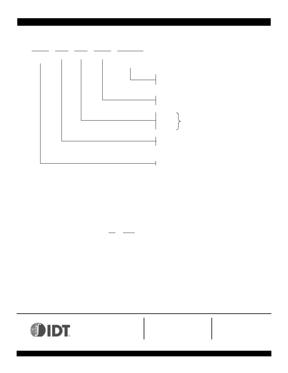
Ordering Information
Ordering Information
Ordering Information
Ordering Information
Data Sheet Document History
Data Sheet Document History
Data Sheet Document History
Data Sheet Document History
4/02/99
Changed format
5/18/99
Changed tDTH from 6ns to 2ns, changed tALPW from 20ns to 40ns, added TxPRTY prop. delay.
6/24/99
Changed tDCH and tDCL from 8ns to 9ns, added tTOV and tROV min of 1ns.
7/06/99
Changed tPTCLK from 11ns to 20ns to match RCLK.
2/12/01
Changed to Final. Made general corrections. No parameters changed.
6/24/02
Added drawing 4308d31, System Clock to RST and LCRST Setup Time. Added tPRSTS and tPRSTH timing to timing parameters table. Changed
e-mail URL from atmhelp@idt.com to switchstarhelp@idt.com.
A
Power
999
Speed
A
Package
A
Process/
Temperature
Range
Blank
Commercial (0 Degrees C to +70 Degrees C)
PQF
PQFP (80-pin)
155
L
Low Power
XXXXX
Device
Type
UTOPIA 1 TO DATA PATH INTERFACE (DPI)
TRANSLATION DEVICE
77010
IDT
4308 drw
4-bit Port Bandwidth in Mbps