
1 of 59
May 25, 2004
© 2004 Integrated Device Technology, Inc.
DSC 6148
IDT and the IDT logo are registered trademarks of Integrated Device Technology, Inc.
Features
32-bit CPU Core
≠ MIPS32 instruction set
≠ Cache Sizes: 16KB instruction and data caches, 4-Way set
associative, cache line locking, non-blocking prefetches
≠ 16 dual-entry JTLB with variable page sizes
≠ 3-entry instruction TLB
≠ 3-entry data TLB
≠ Max issue rate of one 32x16 multiply per clock
≠ Max issue rate of one 32x32 multiply every other clock
≠ CPU control with start, stop and single stepping
≠ Software breakpoints support
≠ Hardware breakpoints on virtual addresses
≠ Enhanced JTAG and ICE Interface that is compatible with v2.5
of the EJTAG Specification
DDR Memory Controller
≠ Supports up to 2GB of DDR SDRAM
≠ 2 chip selects (each chip select supports 4 internal DDR
banks)
≠ Supports 16-bit or 32-bit data bus width using 8, 16, or 32-bit
devices
≠ Supports 64Mb, 128Mb, 256Mb, 512Mb, and 1Gb DDR
SDRAM devices
≠ Data bus multiplexing support allows interfacing to standard
DDR DIMMs and SODIMMs
≠ Automatic refresh generation
Memory and Peripheral Device Controller
≠ Provides "glueless" interface to standard SRAM, Flash, ROM,
dual-port memory, and peripheral devices
≠ Demultiplexed address and data buses: 16-bit data bus, 26-bit
address bus, 6 chip selects, supports alternate bus masters,
control for external data bus buffers
≠ Supports 8-bit and 16-bit width devices
Automatic byte gathering and scattering
≠ Flexible protocol configuration parameters: programmable
number of wait states (0 to 63), programmable postread/post-
write delay (0 to 31), supports external wait state generation,
supports Intel and Motorola style peripherals
≠ Write protect capability per chip select
≠ Programmable bus transaction timer generates warm reset
when counter expires
≠ Supports up to 64 MB of memory per chip select
Counter/Timers
≠ Three general purpose 32-bit counter timers
PCI Interface
≠ 32-bit PCI revision 2.2 compliant (3.3V only)
≠ Supports host or satellite operation in both master and target
modes
≠ Support for synchronous and asynchronous operation
≠ PCI clock supports frequencies from 16 MHz to 66 MHz
≠ PCI arbiter in Host mode: supports 6 external masters, fixed
priority or round robin arbitration
≠ I
2
O "like" PCI Messaging Unit
Block Diagram
EJTAG
MMU
D. Cache
I. Cache
MIPS-32
CPU Core
ICE
Interrupt
Controller
3 Counter
Timers
DMA
Controller
Arbiter
DDR
DDR &
Device
2 UARTS
(16550)
GPIO
Interface
PCI
Master/Target
Memory &
Peripheral Bus
Ch. 1 Ch. 2
Serial Channels
GPIO Pins
PCI Bus
Controller
Controller
SPI
I
2
C
SPI Bus
I
2
C Bus
:
:
10/100
2 Ethernet
Interfaces
MII
MII
IPBus
TM
Interface
PCI Arbiter
(Host Mode)
Controllers
On-Chip
Memory
79RC32438
IDT
TM
Interprise
TM
Integrated
Communications Processor

2 of 59
May 25, 2004
IDT 79RC32438
DMA Controller
≠ 10 DMA channels: two channels for PCI (PCI to Memory and
Memory to PCI), two for each Ethernet interface, two channels
for memory to memory operations, two channels for external
operations
≠ Provides flexible descriptor based operation
≠ Supports unaligned transfers (i.e., source or destination
address may be on any byte boundary) with arbitrary byte
length.
Two Ethernet Interfaces
≠ 10 and 100 Mb/s ISO/IEC 8802-3:1996 compliant
≠ Two IEEE 802.3u compatible Media Independent Interfaces
(MII) with serial management interface
≠ MII supports IEEE 802.3u auto-negotiation speed selection
≠ Supports 64 entry hash table based multicast address filtering
≠ 512 byte transmit and receive FIFOs
≠ Supports flow control functions outlined in IEEE Std. 802.3x-
1997
Universal Asynchronous Receiver Transmitter (UART)
≠ Compatible with the 16550 and 16450 UARTs
≠ Two completely separate serial channels
≠ Modem control functions (CTS, RTS, DSR, DTR, RI, DCD)
≠ 16-byte transmit and receive buffers
≠ Programmable baud rate generator derived from the system
clock
≠ Fully programmable serial characteristics:
≠ 5, 6, 7, or 8 bit characters
≠ Even, odd or no parity bit generation and detection
≠ 1, 1-1/2 or 2 stop bit generation
≠ Line break generation and detection
≠ False start bit detection
≠ Internal loopback mode
I
2
C-Bus
≠ Supports standard 100 Kbps mode as well as 400 Kbps fast
mode
≠ Supports 7-bit and 10-bit addressing
≠ Supports four modes: master transmitter, master receiver,
slave transmitter, slave receiver
Additional General Purpose Peripherals
≠ Two 16550-compatible serial ports
≠ Interrupt controller
≠ System integrity functions
≠ General purpose I/O controller
≠ Serial peripheral interface (SPI)
On-chip Memory
≠ 4KB of high speed SRAM organized as 1K x 32 bits
≠ Supports burst and non-burst byte, halfword, triple-byte, and
word CPU, PCI, and DMA accesses
Debug Support
≠ Rev. 2.6 compliant EJTAG Interface
Device Overview
The RC32438 is a member of the IDTTM InterpriseTM family of PCI
integrated communications processors. It incorporates a high perfor-
mance CPU core and a number of on-chip peripherals. The integrated
processor is designed to transfer information from I/O modules to main
memory with minimal CPU intervention using a highly sophisticated
direct memory access (DMA) engine. All data transfers through the
RC32438 are achieved by writing data from an on-chip I/O peripheral to
main memory and then out to another I/O module.
CPU Execution Core
The 32-bit CPU core is 100% compatible with the MIPS32 instruction
set architecture (ISA).
Specifically, this device features the 4Kc CPU core developed by
MIPS Technologies Inc. (www.mips.com). This core issues a single
instruction per cycle, includes a five stage pipeline, and is optimized for
applications that require integer arithmetic. The CPU core includes 16
KB instruction and 16 KB data caches. Both caches are 4-way set asso-
ciative and can be locked on a per line basis, which allows the
programmer control over this precious on-chip memory resource. The
core also features a memory management unit (MMU). The CPU core
also incorporates an enhanced joint test access group (EJTAG) inter-
face that is used to interface to in-circuit emulator tools, providing
access to internal registers and enabling the part to be controlled exter-
nally, simplifying the system debug process. The use of this core allows
IDT's customers to leverage the broad range of software and develop-
ment tools available for the MIPS architecture, including operating
systems, compilers, and in-circuit emulators.
Double Data Rate Memory Controller
The RC32438 incorporates a high performance double data rate
(DDR) memory controller which supports both x16 and x32 memory
configurations up to 2GB. This module provides all of the signals
required to interface to both memory modules and discrete devices,
including two chip selects, differential clocking outputs and data strobes.
Memory and I/O Controller
The RC32438 uses a dedicated local memory/IO controller including
a de-multiplexed 16-bit data and 26-bit address bus. It includes all of the
signals required to interface directly to as many as six Intel or Motorola-
style external peripherals, and the interface can be configured to
support both 8-bit and 16-bit peripherals.
DMA Controller
The DMA controller consists of 10 independent DMA channels, all of
which operate in exactly the same manner. The DMA controller off-loads
the CPU core from moving data among the on-chip interfaces, external
peripherals, and memory. The controller supports scatter/gather DMA
with no alignment restrictions, appropriate for communications and
graphics systems.
PCI Interface
The PCI interface on the RC32438 is compatible with version 2.2 of
the PCI specification. An on-chip arbiter supports up to six external bus
masters, supporting both fixed priority and rotating priority arbitration
schemes. The part can support both satellite and host PCI configura-
tions, enabling the RC32438 to act as a slave controller for a PCI add-in

3 of 59
May 25, 2004
IDT 79RC32438
card application, or as the primary PCI controller in the system. The PCI
interface can be operated synchronously or asynchronously to the other
I/O interfaces on the RC32438 device.
Ethernet Interface
The RC32438 has two Ethernet Channels supporting 10Mbps and
100Mbps speeds to provide a standard media independent interface
(MII) off-chip, allowing a wide range of external devices to be connected
efficiently.
UART Interface
The RC32438 contains two completely separate serial channels
(UARTs) that are compatible with the industry standard 16550 UART.
System Integrity Functions
The RC32438 contains a programmable watchdog timer that gener-
ates NMI when the counter expires and an address space monitor that
reports errors in response to accesses to undecoded address regions.
General Purpose I/O Controller
The RC32438 contains 32 general purpose input/output pins. Each
pin may be used as an active high or active low level interrupt or non-
maskable interrupt input, and each signal may be used as a bit input or
output port.
I
2
C Interface
The standard I2C interface allows the RC32438 to connect to a
number of standard external peripherals for a more complete system
solution. The RC32438 supports both master and slave operations.
Debug Support
The RC32438 supports the industry standard Rev. 2.6 EJTAG inter-
face.
Thermal Considerations
The RC32438 consumes less than 2.7 W peak power. It is guaran-
teed in a ambient temperature range of 0
∞ to +70∞ C for commercial
temperature devices and - 40
∞ to +85∞ for industrial temperature
devices.
Revision History
November 7, 2002: Initial publication. Preliminary Information.
November 15, 2002: Added footnotes to Tables 5, 9, and 10.
December 12, 2002: Added Clock Speed parameter to PLL and
Core supply in Table 16.
December 19, 2002: Release version.
January 13, 2003: Changed Thermal Considerations to read less
than 2.7W instead of 2.5W, added values to CLK parameter in Table 5,
and revised EJTAG description.
February 4, 2003: Revised description for EJTAG/JTAG pins in
Table 1. Changed DDRDM[7:0] from input/output to output only in Tables
1 and 2 and Logic Diagram. Added new section, Voltage Sense Signal
Timing, as part of EJTAG description.
March 4, 2003: In Table 2, removed "pull-up" from PCI pin category
and from GPIO [24] and GPIO[30-26]. In Table 20, changed max. values
for VccSI/O, VccCore, and VccPLL.
July 9, 2003: In Table 7: changed values for DDRDATA, DDRDM,
and DDRADDR--WEN signals, and deleted old footnote #3 and
changed values in new footnote #3. In Table 8, changed Tdo values.
Changed Figure 7. Changed values in Table 18, Power Consumption.
Removed IPBus Monitor feature which included changes to Tables 1, 2,
21, 24, and 25. Deleted Table 13 which resulted in a re-ordering of
subsequent tables.
March 8, 2004: Added 300MHz speed grade.
May 25, 2004: In Table 9, signals MIIxRXCLK and MIIxTXCLK, the
Min and Max values for Thigh/Tlow_9c were changed to 140 and 260
respectively and the Min and Max values for Thigh/Tlow_9d were
changed to 14.0 and 26.0 respectively.

4 of 59
May 25, 2004
IDT 79RC32438
Pin Description Table
The following table lists the functions of the pins provided on the RC32438. Some of the functions listed may be multiplexed onto the same pin.
The active polarity of a signal is defined using a suffix. Signals ending with an "N" are defined as being active, or asserted, when at a logic zero
(low) level. All other signals (including clocks, buses and select lines) will be interpreted as being active, or asserted when at a logic one (high) level.
Signal
Type
Name/Description
System
CLK
I
Master Clock. This is the master clock input. The processor frequency is a mul-
tiple of this clock frequency. This clock is used as the system clock for all mem-
ory and peripheral bus operations.
EXTCLK
O
External Clock. This clock is used for all memory and peripheral bus opera-
tions.
COLDRSTN
I
Cold Reset. The assertion of this signal initiates a cold reset. This causes the
processor state to be initialized, boot configuration to be loaded, and the internal
PLL to lock onto the master clock (CLK).
RSTN
I/O
Reset. The assertion of this bidirectional signal initiates a warm reset. This sig-
nal is asserted by the RC32438 during a warm reset.
Memory and Peripheral Bus
BDIRN
O
External Buffer Direction. Memory and peripheral bus external data bus buffer
direction control. If the RC32438 memory and peripheral bus is connected to the
A side of a transceiver, such as an IDT74FCT245, then this pin may be directly
connected to the direction control (e.g., BDIR) pin of the transceiver.
BGN
O
Bus Grant. This signal is asserted by the RC32438 to indicate that the
RC32438 has relinquished ownership of the memory and peripheral bus.
BOEN
O
External Buffer Enable. This signal provides an output enable control for an
external buffer on the memory and peripheral data bus.
BRN
I
Bus Request. This signal is asserted by an external device to request owner-
ship of the memory and peripheral bus.
BWEN[1:0]
O
Byte Write Enables. These signals are memory and peripheral bus byte write
enable signals.
BWEN[0] corresponds to byte lane MDATA[7:0]
BWEN[1] corresponds to byte lane MDATA[15:8]
CSN[5:0]
O
Chip Selects. These signals are used to select an external device on the mem-
ory and peripheral bus.
MADDR[21:0]
O
Address Bus. 22-bit memory and peripheral bus address bus.
MADDR[25:22] are available as GPIO alternate functions
MDATA[15:0]
I/O
Data Bus. 16-bit memory and peripheral data bus. During a cold reset, these
pins function as inputs that are used to load the boot configuration vector.
OEN
O
Output Enable. This signal is asserted when data should be driven on by an
external device on the memory and peripheral bus.
RWN
O
Read Write. This signal indicates if the transaction on the memory and periph-
eral bus is a read transaction or a write transaction. A high level indicates a read
from an external device. A low level indicates a write to an external device.
Table 1 Pin Description (Part 1 of 9)

5 of 59
May 25, 2004
IDT 79RC32438
WAITACKN
I
Wait or Transfer Acknowledge. When configured as wait, this signal is
asserted during a memory and peripheral bus transaction to extend the bus
cycle. When configured as a transfer acknowledge, this signal is asserted during
a transaction to signal the completion of the transaction.
DDR Bus
DDRADDR[13:0]
O
DDR Address Bus. 14-bit multiplexed DDR bus address bus. This bus is used
to transfer the addresses to the DDR devices.
DDRBA[1:0]
O
DDR Bank Address. These signals are used to transfer the bank address to the
DDRs.
DDRCASN
O
DDR Column Address Strobe. This signal is asserted during DDR transac-
tions.
DDRCKE
O
DDR Clock Enable. The DDR clock enable is asserted during normal DDR
operation. This signal is negated during following a cold reset or during a power
down operation.
DDRCKN[1:0]
O
DDR Negative DDR clock. These signals are the negative clock of the differen-
tial DDR clock pair. Two copies of this output are provided to reduce signal load-
ing.
DDRCKP[1:0]
O
DDR Positive DDR clock. These signals are the positive clock of the differen-
tial DDR clock pair. Two copies of this output are provided to reduce signal load-
ing.
DDRCSN[1:0]
O
DDR Chip Selects. These active low signals are used to select DDR device(s)
on the DDR bus.
DDRDATA[31:0]
I/O
DDR Data Bus. 32-bit DDR data bus used to transfer data between the
RC32438 and the DDR devices. Data is transferred on both edges of the clock.
DDRDM[7:0]
O
DDR Data Write Enables. Byte data write enables used to enable specific byte
lanes during DDR writes.
DDRDM[0] corresponds to DDRDATA[7:0]
DDRDM[1] corresponds to DDRDATA[15:8]
DDRDM[2] corresponds to DDRDATA[23:16]
DDRDM[3] corresponds to DDRDATA[31:24]
DDRDM[4] corresponds to DDRDATA[39:32]
DDRDM[5] corresponds to DDRDATA[47:40]
DDRDM[6] corresponds to DDRDATA[55:48]
DDRDM[7] corresponds to DDRDATA[54:56]
(Refer to the DDR Data Bus Multiplexing section in Chapter 7 of the RC32438
User Reference Manual.)
DDRDQS[3:0]
I/O
DDR Data Strobes. DDR byte data strobes used to clock data between DDR
devices and the RC32438. These strobes are inputs during DDR reads and out-
puts during DDR writes.
DDRDQS[0] corresponds to DDRDATA[7:0].
DDRDQS[1] corresponds to DDRDATA[15:8].
DDRDQS[2] corresponds to DDRDATA[23:16].
DDRDQS[3] corresponds to DDRDATA[31:24].
DDROEN[3:0]
O
DDR Bus Switch Output Enables. These pins are used to enable external
data bus switches in systems that support data bus multiplexing.
DDRRASN
O
DDR Row Address Strobe. The DDR row address strobe is asserted during
DDR transactions.
Signal
Type
Name/Description
Table 1 Pin Description (Part 2 of 9)

6 of 59
May 25, 2004
IDT 79RC32438
DDRVREF
I
DDR Voltage Reference. SSTL_2 DDR voltage reference generated by an
external source.
DDRWEN
O
DDR Write Enable. DDR write enable is asserted during DDR write transac-
tions.
PCI Bus
PCIAD[31:0]
I/O
PCI Multiplexed Address/Data Bus. Address is driven by a bus master during
initial PCIFRAMEN assertion. Data is then driven by the bus master during
writes or by the bus target during reads.
PCICBEN[3:0]
I/O
PCI Multiplexed Command/Byte Enable Bus. PCI command is driven by the
bus master during the initial PCIFRAMEN assertion. Byte enable signals are
driven by the bus master during subsequent data phase(s).
PCICLK
I
PCI Clock. Clock used for all PCI bus transactions.
PCIDEVSELN
I/O
PCI Device Select. This signal is driven by a bus target to indicate that the tar-
get has decoded the address as one of its own address spaces.
PCIFRAMEN
I/O
PCI Frame. Driven by a bus master. Assertion indicates the beginning of a bus
transaction. Negation indicates the last data.
PCIGNTN[3:0]
I/O
PCI Bus Grant.
In PCI host mode with internal arbiter:
The assertion of these signals indicates to the agent that the internal RC32438
arbiter has granted the agent access to the PCI bus.
In PCI host mode with external arbiter:
PCIGNTN[0]: asserted by an external arbiter to indicate to the RC32438 that
access to the PCI bus has been granted.
PCIGNTN[3:1]: unused and driven high.
In PCI satellite mode:
PCIGNTN[0]: This signal is asserted by an external arbiter to indicate to the
RC32438 that access to the PCI bus has been granted.
PCIGNTN[1]: this signal takes on the alternate function of PCIEECS and is used
as a PCI Serial EEPROM chip select
PCIGNTN[3:2]: unused and driven high.
Note: When the GPIO register is programmed in the alternate function mode for
bits GPIO [26] and [28], these bits become PCIGNTN [4] and [5] respectively.
PCIIRDYN
I/O
PCI Initiator Ready. Driven by the bus master to indicate that the current datum
can complete.
PCILOCKN
I/O
PCI Lock. This signal is asserted by an external bus master to indicate that an
exclusive operation is occurring.
PCIPAR
I/O
PCI Parity. Even parity of the PCIAD[31:0] bus. Driven by the bus master during
address and write Data phases. Driven by the bus target during the read data
phase.
PCIPERRN
I/O
PCI Parity Error. If a parity error is detected, this signal is asserted by the
receiving bus agent 2 clocks after the data is received.
Signal
Type
Name/Description
Table 1 Pin Description (Part 3 of 9)
7 of 59
May 25, 2004
IDT 79RC32438
PCIREQN[3:0]
I/O
PCI Bus Request.
In PCI host mode with internal arbiter:
These signals are inputs whose assertion indicates to the internal RC32438
arbiter that an agent desires ownership of the PCI bus.
In PCI host mode with external arbiter:
PCIREQN[0]: asserted by the RC32438 to request ownership of the PCI bus.
PCIREQN[3:1]: unused and driven high.
In PCI satellite mode:
PCIREQN[0]: this signal is asserted by the RC32438 to request use of the PCI
bus.
PCIREQN[1]: function changes to PCIIDSEL and is used as a chip select during
configuration read and write transactions.
PCIREQN[3:2]: unused and driven high.
Note: When the GPIO register is programmed in the alternate function mode for
bits GPIO [24] and [27], these bits become PCIREQN [4] and [5] respectively.
PCIRSTN
I/O
PCI Reset. In host mode, this signal is asserted by the RC32438 to generate a
PCI reset. In satellite mode, assertion of this signal initiates a warm reset.
PCISERRN
I/O
PCI System Error. This signal is driven by an agent to indicate an address par-
ity error, data parity error during a special cycle command, or any other system
error. Requires an external pull-up.
PCISTOPN
I/O
PCI Stop. Driven by the bus target to terminate the current bus transaction. For
example, to indicate a retry.
PCITRDYN
I/O
PCI Target Ready. Driven by the bus target to indicate that the current data can
complete.
General Purpose Input/Output
GPIO[0]
I/O
General Purpose I/O.
This pin can be configured as a general purpose I/O pin.
Alternate function pin name: U0SOUT
Alternate function: UART channel 0 serial output.
GPIO[1]
I/O
General Purpose I/O.
This pin can be configured as a general purpose I/O pin.
Alternate function pin name: U0SINP
Alternate function: UART channel 0 serial input.
GPIO[2]
I/O
General Purpose I/O.
This pin can be configured as a general purpose I/O pin.
Alternate function pin name: U0RIN
Alternate function: UART channel 0 ring indicator input.
GPIO[3]
I/O
General Purpose I/O.
This pin can be configured as a general purpose I/O pin.
Alternate function pin name: U0DCDN
Alternate function: UART channel 0 data carrier detect input.
GPIO[4]
I/O
General Purpose I/O.
This pin can be configured as a general purpose I/O pin.
Alternate function pin name: U0DTRN
Alternate function: UART channel 0 data terminal ready input.
GPIO[5]
I/O
General Purpose I/O.
This pin can be configured as a general purpose I/O pin.
Alternate function pin name: U0DSRN
Alternate function: UART channel 0 data set ready input.
Signal
Type
Name/Description
Table 1 Pin Description (Part 4 of 9)

8 of 59
May 25, 2004
IDT 79RC32438
GPIO[6]
I/O
General Purpose I/O.
This pin can be configured as a general purpose I/O pin.
Alternate function pin name: U0RTSN
Alternate function: UART channel 0 request to send output.
GPIO[7]
I/O
General Purpose I/O.
This pin can be configured as a general purpose I/O pin.
Alternate function pin name: U0CTSN
Alternate function: UART channel 0 clear to send input.
GPIO[8]
I/O
General Purpose I/O.
This pin can be configured as a general purpose I/O pin.
Alternate function pin name: U1SOUT
Alternate function: UART channel 1 serial output.
GPIO[9]
I/O
General Purpose I/O.
This pin can be configured as a general purpose I/O pin.
Alternate function pin name: U1SINP
Alternate function: UART channel 1 serial input.
GPIO[10]
I/O
General Purpose I/O.
This pin can be configured as a general purpose I/O pin.
Alternate function pin name: U1DTRN
Alternate function: UART channel 1 data terminal ready output.
GPIO[11]
I/O
General Purpose I/O.
This pin can be configured as a general purpose I/O pin.
Alternate function pin name: U1DSRN
Alternate function: UART channel 1 data set ready input.
GPIO[12]
I/O
General Purpose I/O.
This pin can be configured as a general purpose I/O pin.
Alternate function pin name: U1RTSN
Alternate function: UART channel 1 request to send output.
GPIO[13]
I/O
General Purpose I/O.
This pin can be configured as a general purpose I/O pin.
Alternate function pin name: U1CTSN
Alternate function: UART channel 1 clear to send input.
GPIO[14]
I/O
General Purpose I/O.
This pin can be configured as a general purpose I/O pin.
Alternate function pin name: DMAREQN0
Alternate function: External DMA channel 0 request input.
GPIO[15]
I/O
General Purpose I/O.
This pin can be configured as a general purpose I/O pin.
Alternate function pin name: DMAREQN1
Alternate function: External DMA channel 1 request input.
GPIO[16]
I/O
General Purpose I/O.
This pin can be configured as a general purpose I/O pin.
Alternate function pin name: DMADONEN0
Alternate function: External DMA channel 0 done input.
GPIO[17]
I/O
General Purpose I/O.
This pin can be configured as a general purpose I/O pin.
Alternate function pin name: DMADONEN1
Alternate function: External DMA channel 1 done input.
Signal
Type
Name/Description
Table 1 Pin Description (Part 5 of 9)

9 of 59
May 25, 2004
IDT 79RC32438
GPIO[18]
I/O
General Purpose I/O.
This pin can be configured as a general purpose I/O pin.
Alternate function pin name: DMAFINN0
Alternate function: External DMA channel 0 finished output.
GPIO[19]
I/O
General Purpose I/O.
This pin can be configured as a general purpose I/O pin.
Alternate function pin name: DMAFINN1
Alternate function: External DMA channel 1 finished output.
GPIO[20]
I/O
General Purpose I/O.
This pin can be configured as a general purpose I/O pin
Alternate function pin name: MADDR[22]
Alternate function: Memory and peripheral bus address output.
GPIO[21]
I/O
General Purpose I/O.
This pin can be configured as a general purpose I/O pin.
Alternate function pin name: MADDR[23]
Alternate function: Memory and peripheral bus address output.
GPIO[22]
I/O
General Purpose I/O.
This pin can be configured as a general purpose I/O pin.
Alternate function pin name: MADDR[24]
Alternate function: Memory and peripheral bus address output.
GPIO[23]
I/O
General Purpose I/O.
This pin can be configured as a general purpose I/O pin.
Alternate function pin name: MADDR[25]
Alternate function: Memory and peripheral bus address output.
GPIO[24]
I/O
General Purpose I/O.
This pin can be configured as a general purpose I/O pin.
Alternate function pin name: PCIREQN[4]
Alternate function: PCI Request 4 input or output.
GPIO[25]
I/O
General Purpose I/O.
This pin can be configured as a general purpose I/O pin.
Alternate function pin name: AFSPARE1
Alternate function: reserved.
GPIO[26]
I/O
General Purpose I/O.
This pin can be configured as a general purpose I/O pin.
Alternate function pin name: PCIGNTN[4]
Alternate function: PCI Grant 4 output.
GPIO[27]
I/O
General Purpose I/O.
This pin can be configured as a general purpose I/O pin.
Alternate function pin name: PCIREQN[5]
Alternate function: PCI Request 5 input or output.
GPIO[28]
I/O
General Purpose I/O.
This pin can be configured as a general purpose I/O pin.
Alternate function pin name: PCIGNTN[5]
Alternate function: PCI Grant 5 output.
GPIO[29]
I/O
General Purpose I/O.
This pin can be configured as a general purpose I/O pin.
Alternate function pin name: Reserved
Alternate function: Reserved.
Signal
Type
Name/Description
Table 1 Pin Description (Part 6 of 9)

10 of 59
May 25, 2004
IDT 79RC32438
GPIO[30]
I/O
General Purpose I/O.
This pin can be configured as a general purpose I/O pin.
Alternate function pin name: PCIMUINTN
Alternate function: PCI Messaging unit interrupt output.
GPIO[31]
I/O
General Purpose I/O.
This pin can be configured as a general purpose I/O pin.
SPI Interface
SCK
I/O
Serial Clock. This signal is used as the serial clock output in SPI mode and in
PCI satellite mode with suspended CPU execution during PCI serial EEPROM
loading. This pin may be configured as a GPIO pin.
SDI
I/O
Serial Data Input. This signal is used to shift in serial data in SPI mode and in
PCI satellite mode with suspended CPU execution during PCI serial EEPROM
loading. This pin may be configured as a GPIO pin.
SDO
I/O
Serial Data Output. This signal is used shift out serial data in SPI mode and in
PCI satellite mode with suspended CPU execution during PCI serial EEPROM
loading. This pin may be configured as a GPIO pin.
I
2
C Bus Interface
SCL
I/O
I
2
C Clock. I
2
C-bus clock.
SDA
I/O
I
2
C Data Bus. I
2
C-bus data bus.
Ethernet Interfaces
MII0CL
I
Ethernet 0 MII Collision Detected. This signal is asserted by the ethernet PHY
when a collision is detected.
MII0CRS
I
Ethernet 0 MII Carrier Sense. This signal is asserted by the ethernet PHY
when either the transmit or receive medium is not idle.
MII0RXCLK
I
Ethernet 0 MII Receive Clock. This clock is a continuous clock that provides a
timing reference for the reception of data.
MII0RXD[3:0]
I
Ethernet 0 MII Receive Data. This nibble wide data bus contains the data
received by the ethernet PHY.
MII0RXDV
I
Ethernet 0 MII Receive Data Valid. The assertion of this signal indicates that
valid receive data is in the MII receive data bus.
MII0RXER
I
Ethernet 0 MII Receive Error. The assertion of this signal indicates that an
error was detected somewhere in the ethernet frame currently being sent in the
MII receive data bus.
MII0TXCLK
I
Ethernet 0 MII Transmit Clock. This clock is a continuous clock that provides a
timing reference for the transfer of transmit data.
MII0TXD[3:0]
O
Ethernet 0 MII Transmit Data. This nibble wide data bus contains the data to
be transmitted.
MII0TXENP
O
Ethernet 0 MII Transmit Enable. The assertion of this signal indicates that data
is present on the MII for transmission.
MII0TXER
O
Ethernet 0 MII Transmit Coding Error. When this signal is asserted together
with MIITXENP, the ethernet PHY will transmit symbols which are not valid data
or delimiters.
MII1CL
I
Ethernet 1 MII Collision Detected. This signal is asserted by the ethernet PHY
when a collision is detected.
Signal
Type
Name/Description
Table 1 Pin Description (Part 7 of 9)

11 of 59
May 25, 2004
IDT 79RC32438
MII1CRS
I
Ethernet 1 MII Carrier Sense. This signal is asserted by the ethernet PHY
when either the transmit or receive medium is not idle.
MII1RXCLK
I
Ethernet 1 MII Receive Clock. This clock is a continuous clock that provides a
timing reference for the reception of data.
MII1RXD[3:0]
I
Ethernet 1 MII Receive Data. This nibble wide data bus contains the data
received by the ethernet PHY.
MII1RXDV
I
Ethernet 1 MII Receive Data Valid. The assertion of this signal indicates that
valid receive data is in the MII receive data bus.
MII1RXER
I
Ethernet 1 MII Receive Error. The assertion of this signal indicates that an
error was detected somewhere in the ethernet frame currently being sent in the
MII receive data bus.
MII1TXCLK
I
Ethernet 1 MII Transmit Clock. This clock is a continuous clock that provides a
timing reference for the transfer of transmit data.
MII1TXD[3:0]
O
Ethernet 1 MII Transmit Data. This nibble wide data bus contains the data to
be transmitted.
MII1TXENP
O
Ethernet 1 MII Transmit Enable. The assertion of this signal indicates that data
is present on the MII for transmission.
MII1TXER
O
Ethernet 1 MII Transmit Coding Error. When this signal is asserted together
with MIITXENP, the ethernet PHY will transmit symbols which are not valid data
or delimiters.
MIIMDC
O
MII Management Data Clock. This signal is used as a timing reference for
transmission of data on the management interface.
MIIMDIO
I/O
MII Management Data. This bidirectional signal is used to transfer data
between the station management entity and the ethernet PHY.
JTAG / EJTAG
EJTAG_TMS
I
EJTAG Mode. The value on this signal controls the test mode select of the
EJTAG Controller. When using the JTAG boundary scan, this pin should be left
disconnected (since there is an internal pull-up) or driven high.
JTAG_TCK
I
JTAG Clock. This is an input test clock used to clock the shifting of data into or
out of the boundary scan logic, JTAG Controller, or the EJTAG Controller.
JTAG_TCK is independent of the system and the processor clock with a nomi-
nal 50% duty cycle.
JTAG_TDI
I
JTAG Data Input. This is the serial data input to the boundary scan logic, JTAG
Controller, or the EJTAG Controller.
JTAG_TDO
O
JTAG Data Output. This is the serial data shifted out from the boundary scan
logic, JTAG Controller, or the EJTAG Controller. When no data is being shifted
out, this signal is tri-stated.
JTAG_TMS
I
JTAG Mode. The value on this signal controls the test mode select of the
boundary scan logic or JTAG Controller. When using the EJTAG debug inter-
face, this pin should be left disconnected (since there is an internal pull-up) or
driven high.
Signal
Type
Name/Description
Table 1 Pin Description (Part 8 of 9)

12 of 59
May 25, 2004
IDT 79RC32438
Pin Characteristics
Note: Some input pads of the RC32438 do not contain internal pull-ups or pull-downs. Unused inputs should be tied off to appropriate
levels. This is especially critical for unused control signal inputs (such as BRN) which, if left floating, could adversely affect the RC32438's
operation. Also, any input pin left floating can cause a slight increase in power consumption.
JTAG_TRST_N
I
JTAG Reset. This active low signal asynchronously resets the boundary scan
logic, JTAG TAP Controller, and the EJTAG Debug TAP Controller. An external
pull-up on the board is recommended to meet the JTAG specification in cases
where the tester can access this signal. However, for systems running in func-
tional mode, one of the following should occur:
1) actively drive this signal low with control logic
2) statically drive this signal low with an external pull-down on the board
3) clock JTAG_TCK while holding EJTAG_TMS and/or JTAG_TMS high.
Debug
CPU
O
CPU Transaction. This signal is asserted during all CPU instruction fetches and
data transfers to/from the DDR and devices on the memory and peripheral bus.
The signal is negated during PCI and DMA transactions to/from the DDR and
devices on the memory and peripheral bus.
INST
O
Instruction or Data. This signal is driven high during CPU instruction fetches on
the memory and peripheral bus memory or DDR bus.
Function
Pin Name
Type Buffer
I/O Type
Internal
Resistor
Notes
1
Memory and
Peripheral Bus
BDIRN
O
LVTTL
High Drive
BGN
O
LVTTL
Low Drive
BOEN
O
LVTTL
High Drive
BRN
I
LVTTL
STI
2
pull-up
BWEN[1:0]
O
LVTTL
High Drive
CSN[5:0]
O
LVTTL
High Drive
MADDR[21:0]
O
LVTTL
High Drive
MDATA[15:0]
I/O
LVTTL
High Drive
OEN
O
LVTTL
High Drive
RWN
O
LVTTL
High Drive
WAITACKN
I
LVTTL
STI
pull-up
Table 2 Pin Characteristics (Part 1 of 4)
Signal
Type
Name/Description
Table 1 Pin Description (Part 9 of 9)
13 of 59
May 25, 2004
IDT 79RC32438
DDR Bus
DDRADDR[13:0]
O
SSTL_2
SSTL_2
DDRBA[1:0]
O
SSTL_2
SSTL_2
DDRCASN
O
SSTL_2
SSTL_2
DDRCKE
O
SSTL_2 /
LVCMOS
SSTL_2
DDRCKN[1:0]
O
SSTL_2
SSTL_2
DDRCKP[1:0]
O
SSTL_2
SSTL_2
DDRCSN[1:0]
O
SSTL_2
SSTL_2
DDRDATA[31:0]
I/O
SSTL_2
SSTL_2
DDRDM[7:0]
O
SSTL_2
SSTL_2
DDRDQS[3:0]
I/O
SSTL_2
SSTL_2
DDROEN[3:0]
O
SSTL_2
SSTL_2
DDRRASN
O
SSTL_2
SSTL_2
DDRVREF
I
Analog
SSTL_2
DDRWEN
O
SSTL_2
SSTL_2
PCI Bus Interface
3
PCIAD[31:0]
I/O
PCI
PCI
PCICBEN[3:0]
I/O
PCI
PCI
PCICLK
I
PCI
PCI
PCIDEVSELN
I/O
PCI
PCI
pull-up on board
PCIFRAMEN
I/O
PCI
PCI
pull-up on board
PCIGNTN[3:0]
I/O
PCI
PCI
pull-up on board
PCIIRDYN
I/O
PCI
PCI
pull-up on board
PCILOCKN
I/O
PCI
PCI
PCIPAR
I/O
PCI
PCI
PCIPERRN
I/O
PCI
PCI
PCIREQN[3:0]
I/O
PCI
PCI
pull-up on board
PCIRSTN
I/O
PCI
PCI
pull-down on board
PCISERRN
I/O
PCI
Open Collec-
tor; PCI
pull-up on board
PCISTOPN
I/O
PCI
PCI
pull-up on board
PCITRDYN
I/O
PCI
PCI
pull-up on board
General Purpose
I/O
GPIO[23:0]
I/O
LVTTL
Low Drive
pull-up
GPIO[24]
I/O
PCI
pull-up on board
GPIO[25]
I/O
LVTTL
Low Drive
pull-up
GPIO[30:26]
4
I/O
PCI
pull-up on board
GPIO[31]
I/O
LVTTL
Low Drive
pull-up
Function
Pin Name
Type Buffer
I/O Type
Internal
Resistor
Notes
1
Table 2 Pin Characteristics (Part 2 of 4)
14 of 59
May 25, 2004
IDT 79RC32438
Serial Interface
SCK
I/O
LVTTL
Low Drive
pull-up
pull-up on board
SDI
I/O
LVTTL
Low Drive
pull-up
pull-up on board
SDO
I/O
LVTTL
Low Drive
pull-up
pull-up on board
I
2
C-Bus Interface
SCL
I/O
LVTTL
Low Drive/STI
pull-up on board
5
SDA
I/O
LVTTL
Low Drive/STI
pull-up on board
5
Ethernet Interfaces MII0CL
I
LVTTL
STI
pull-down
MII0CRS
I
LVTTL
STI
pull-down
MII0RXCLK
I
LVTTL
STI
pull-up
MII0RXD[3:0]
I
LVTTL
STI
pull-up
MII0RXDV
I
LVTTL
STI
pull-down
MII0RXER
I
LVTTL
STI
pull-down
MII0TXCLK
I
LVTTL
STI
pull-up
MII0TXD[3:0]
O
LVTTL
Low Drive
MII0TXENP
O
LVTTL
Low Drive
MII0TXER
O
LVTTL
Low Drive
MII1CL
I
LVTTL
STI
pull-down
MII1CRS
I
LVTTL
STI
pull-down
MII1RXCLK
I
LVTTL
STI
pull-up
MII1RXD[3:0]
I
LVTTL
STI
pull-up
MII1RXDV
I
LVTTL
STI
pull-down
MII1RXER
I
LVTTL
STI
pull-down
MII1TXCLK
I
LVTTL
STI
pull-up
MII1TXD[3:0]
O
LVTTL
Low Drive
MII1TXENP
O
LVTTL
Low Drive
MII1TXER
O
LVTTL
Low Drive
MIIMDC
O
LVTTL
Low Drive
MIIMDIO
I/O
LVTTL
Low Drive
pull-up
EJTAG / ICE
JTAG_TRST_N
I
LVTTL
STI
pull-up
JTAG_TCK
I
LVTTL
STI
pull-up
JTAG_TDI
I
LVTTL
STI
pull-up
JTAG_TDO
O
LVTTL
Low Drive
JTAG_TMS
I
LVTTL
STI
pull-up
EJTAG_TMS
I
LVTTL
STI
pull-up
Debug
CPU
O
LVTTL
Low Drive
INST
O
LVTTL
Low Drive
Function
Pin Name
Type Buffer
I/O Type
Internal
Resistor
Notes
1
Table 2 Pin Characteristics (Part 3 of 4)

15 of 59
May 25, 2004
IDT 79RC32438
Boot Configuration Vector
The boot configuration vector is read by the RC32438 during a cold reset. The vector defines essential RC32438 parameters that are required
once the cold reset completes.
The encoding of the boot configuration vector is described in Table 3, and the vector input is illustrated in Figure 4. The value of the boot configura-
tion vector read in by the RC32438 during a cold reset may be determined by reading the Boot Configuration Vector (BCV) Register.
Miscellaneous
CLK
I
LVTTL
STI
EXTCLK
O
LVTTL
High Drive
COLDRSTN
I
LVTTL
STI
RSTN
I/O
LVTTL
Low Drive / STI
pull-up
pull-up on board
1.
External pull-up required in most system applications. Some applications may require additional pull-ups not identified in this table.
2.
Schmidt Trigger Input (STI).
3.
The PCI pins have internal pull-ups but they are too weak to guarantee system validity. Therefore, board pull-ups are mandatory
where indicated. GPIO alternate function pins for PCI must also have board pull-ups.
4.
PCIMUINTN is an alternate function of GPIO[30]. When configured as an alternate function, this pin is tri-stated when not asserted
(i.e., it acts as an open collector output).
5.
Use a 2.2K pull-up resistor for I2C pins.
Signal
Name/Description
MDATA[3:0]
CPU Pipeline Clock Multiplier. This field specifies the value by which the PLL multi-
plies the master clock input (CLK) to obtain the processor clock frequency (PCLK). For
master clock input frequency constraints, refer to Table 3.1 in the RC32438 User Man-
ual.
0x0 - PLL Bypass
0x1 - Multiply by 3
0x2 - Multiply by 4
0x3 - Multiply by 6
0x4 - Multiply by 8
0x5 - reserved
0x6 - reserved
0x7 - reserved
0x8 - reserved
0xD - reserved
0xE - reserved
0xF - reserved
MDATA[5:4]
External Clock Divider. This field specifies the value by which the IPBus clock
(ICLK), which is always 1/2 PCLK, is divided in order to generate the external clock
output on the EXTCLK pin.
0x0 - Divide by 1
0x1 - Divide by 2
0x2 - Divide by 4
0x3 - reserved
MDATA[6]
Endian. This bit specifies the endianness.
0x0 - little endian
0x1 - big endian
Table 3 Boot Configuration Encoding (Part 1 of 2)
Function
Pin Name
Type Buffer
I/O Type
Internal
Resistor
Notes
1
Table 2 Pin Characteristics (Part 4 of 4)

16 of 59
May 25, 2004
IDT 79RC32438
MDATA[7]
Boot Device Width. This field specifies the width of the boot device (i.e., Device 0).
0x0 - 8-bit boot device width
0x1 - 16-bit boot device width
MDATA[8]
Reset Mode. This bit specifies the length of time the RSTN signal is driven.
0x0 - Normal reset: RSTN driven for minimum of 4096 clock cycles
0x1 - reserved
MDATA[11:9]
PCI Mode. This bit controls the operating mode of the PCI bus interface. The initial
value of the EN bit in the PCIC register is determined by the PCI mode.
0x0 - Disabled (EN initial value is zero)
0x1 - PCI satellite mode with PCI target not ready (EN initial value is one)
0x2 - PCI satellite mode with suspended CPU execution (EN initial value is one)
0x3 - PCI host mode with external arbiter (EN initial value is zero)
0x4 - PCI host mode with internal arbiter using fixed priority arbitration algorithm
(EN initial value is zero)
0x5 - PCI host mode with internal arbiter using round robin arbitration algorithm
(EN initial value is zero)
0x6 - reserved
0x7 - reserved
MDATA[12]
Disable Watchdog Timer. When this bit is set, the watchdog timer is disabled follow-
ing a cold reset.
0x0 - Watchdog timer enabled
0x1 - Watchdog timer disabled
MDATA[15:13]
Reserved. These pins must be driven low during boot configuration.
Signal
Name/Description
Table 3 Boot Configuration Encoding (Part 2 of 2)

17 of 59
May 25, 2004
IDT 79RC32438
Logic Diagram -- RC32438
Figure 1 Logic Diagram
Miscellaneous
Signals
Memory
and
Peripheral
Bus
CLK
COLDRSTN
RSTN
4
MIIMDC
MIIMDIO
MII0CL
MII0CRS
MII0RXCLK
MII0RXD[3:0]
MII0RXDV
MII0RXER
MII0TXCLK
MII0TXD[3:0]
MII0TXENP
MII0TXER
MII1CL
MII1CRS
MII1RXCLK
MII1RXD[3:0]
MII1RXDV
MII1RXER
MII1TXCLK
MII1TXD[3:0]
MII1TXENP
MII1TXER
BDIRN
BGN
BOEN
BRN
BWEN[1:0]
CSN[5:0]
MADDR[21:0]
MDATA[15:0]
OEN
RWN
WAITACKN
DDRADDR[13:0]
DDRBA[1:0]
DDRCASN
DDRCKE
DDRCKN[1:0]
DDRCKP[1:0]
DDRCSN[1:0]
DDRDATA[31:0]
DDRDM[7:0]
DDRDQS[3:0]
DDRRASN
DDRVREF
DDRWEN
PCIAD[31:0]
PCICBEN[3:0]
PCICLK
PCIDEVSELN
PCIFRAMEN
PCIGNTN[3:0]
PCIIRDYN
PCILOCKN
PCIPAR
PCIPERRN
PCIREQN[3:0]
PCIRSTN
PCISERRN
PCISTOPN
PCITRDYN
GPIO[31:0]
SDO
SDA
SCL
JTAG_TCK
JTAG_TDI
JTAG_TDO
JTAG_TMS
JTAG_TRST_N
INST
CPU
4
4
4
32
4
4
4
32
4
8
32
2
2
2
2
14
16
22
6
2
EJTAG / JTAG
Signals
Debug
Signals
General Purpose
I/O
I
2
C-Bus
Serial I/O
PCI Bus
DDR Bus
Ethernet
RC32438
VccCore
VccI/O
Vss
VccPLL
VssPLL
Power/Ground
SDI
SCK
DDROEN[3:0]
4
EJTAG_TMS
EXTCLK

18 of 59
May 25, 2004
IDT 79RC32438
AC Timing Definitions
Below are examples of the AC timing characteristics used throughout this document.
Figure 2 AC Timing Definitions Waveform
Symbol
Definition
Tper
Clock period.
Tlow
Clock low. Amount of time the clock is low in one clock period.
Thigh
Clock high. Amount of time the clock is high in one clock period.
Trise
Rise time. Low to high transition time.
Tfall
Fall time. High to low transition time.
Tjitter
Jitter. Amount of time the reference clock (or signal) edge can vary on either the rising or falling edges.
Tdo
Data out. Amount of time after the reference clock edge that the output will become valid. The minimum time represents the data output hold.
The maximum time represents the earliest time the designer can use the data.
Tzd
Z state to data valid. Amount of time after the reference clock edge that the tri-stated output takes to become valid.
Tdz
Data valid to Z state. Amount of time after the reference clock edge that the valid output takes to become tri-stated.
Tsu
Input set-up. Amount of time before the reference clock edge that the input must be valid.
Thld
Input hold. Amount of time after the reference clock edge that the input must remain valid.
Tpw
Pulse width. Amount of time the input or output is active for asynchronous signals.
Tslew
Slew rate. The rise or fall rate for a signal to go from a high to low, or low to high.
X(clock)
Timing value. This notation represents a value of `X' multiplied by the clock time period of the specified clock. Using 5(CLK) as an example:
X = 5 and the oscillator clock (CLK) = 25MHz, then the timing value is 200.
Tskew
Skew. The amount of time two signal edges deviate from one another.
Table 4 AC Timing Definitions
Tdz
Tzd
Tdo
Tpw
Tpw
Thld
Tsu
Tlow
Thigh
Thigh
Tper
clock
Output signal 1
Output signal 2
Input Signal 1
Signal 1
Tjitter
Trise
Tfall
Tdo
Signal 2
Signal 3
Tskew

19 of 59
May 25, 2004
IDT 79RC32438
System Clock Parameters
Values based on systems running at recommended supply voltages and operating temperatures, as shown in Tables 15 and 16.
Figure 3 Clock Parameters Waveform
Parameter
Symbol
Reference
Edge
200MHz
233MHz
266MHz
300MHz
Units
Timing
Diagram
Reference
Min
Max
Min
Max
Min
Max
Min
Max
PCLK
1
1.
The CPU pipeline clock (PCLK) speed is selected during cold reset by the boot configuration vector (see Table 3).
Frequency
none
200
200
200
233
200
266
200
300
MHz
See Figure 3.
Tper
5.0
5.0
4.2
5.0
3.8
5.0
3.3
5.0
ns
ICLK
2,3,4
2.
ICLK is the internal IPBus clock. It is always equal to PCLK divided by 2. This clock cannot be sampled externally.
3.
The ethernet clock (MIIxRXCLK and MIIxTXCLK) frequency must be equal to or less than 1/2 ICLK (MIIxRXCLK and MIIxTXCLK <= 1/2(ICLK)).
4.
PCICLK must be equal to or less than two times ICLK (PCICLK <= 2(ICLK)) with a maximum PCICLK of 66MHz.
Frequency
none
100
100
100
116.5
100
133
100
150
MHz
Tper
10.0
10.0
10.0
8.5
10.0
7.5
6.7
10.0
ns
CLK
5
5.
The input clock (CLK) is input from the external oscillator to the internal PLL.
Frequency
none
25
66.6
25
77.6
25
88.6
25
100
MHz
Tper_5a
15.0
40.0
12.9
40.0
11.2
40.0
10
40
ns
Thigh_5a,
Tlow_5a
40
60
40
60
40
60
40
60
% of
Tper_5a
Trise_5a,
Tfall_5a
--
3.0
--
3.0
--
3.0
--
3.0
ns
Tjitter_5a
--
0.1
--
0.1
--
0.1
--
0.1
ns
Table 5 Clock Parameters
Tlow_5a
Thigh_5a
Tper_5a
CLK
Trise_5a
Tfall_5a
Tjitter_5a
Tjitter_5a
20 of 59
May 25, 2004
IDT 79RC32438
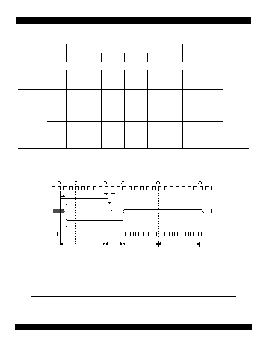
AC Timing Characteristics
Values given below are based on systems running at recommended operating temperatures and supply voltages, shown in Tables 15 and 16.
Figure 4 Cold Reset AC Timing Waveform
Signal
Symbol Reference
Edge
200MHz
233MHz
266MHz
300MHz
Unit Conditions
Timing
Diagram
Reference
Min
Max
Min
Max
Min
Max
Min
Max
Reset
COLDRSTN
1
1.
The COLDRSTN minimum pulse width is the oscillator stabilization time (OSC) plus 0.5 ms with V
cc
stable.
Tpw_6a
2
2.
The values for this symbol were determined by calculation, not by testing.
none
OSC +
0.5
--
OSC +
0.5
--
OSC +
0.5
--
OSC +
0.5
--
ms
Cold reset
See Figures 4
and 5.
Trise_6a none
--
5.0
--
5.0
--
5.0
--
5.0
ns
Cold reset
RSTN
3
(input)
Tpw_6b
2
none
2(CLK)
--
2(CLK)
--
2(CLK)
--
2(CLK)
--
ns
Warm reset
RSTN
3
(output)
3.
RSTN is a bidirectional signal. It is treated as an asynchronous input.
Tdo_6c
COLDRSTN
falling
--
15.0
--
15.0
--
15.0
--
15.0
ns
Cold reset
MDATA[15:0]
(boot vector)
Thld_6d
COLDRSTN
rising
3.0
--
3.0
--
3.0
--
3.0
--
ns
Cold reset
Tdz_6d
2
COLDRSTN
falling
--
30.0
--
30.0
--
30.0
--
30.0
ns
Cold reset
Tdz_6d
2
RSTN falling
--
5(CLK)
--
5(CLK)
--
5(CLK)
--
5(CLK)
ns
Warm reset
Tzd_6d
2
RSTN rising
2(CLK)
--
2(CLK)
--
2(CLK)
--
2(CLK)
--
ns
Warm reset
Table 6 Reset and System AC Timing Characteristics
BOOT VECT
CLK
COLDRSTN
RSTN
MDATA[15:0]
BDIRN
BOEN
Tpw_6a
>= 4096 CLK clock cycles
1
2
3
4
5
6
FFFF_FFFF
1.
COLDRSTN asserted by external logic. The RC32438 asserts RSTN, asserts BOEN low, drives BDIRN low, disables EXTCLK, and tri-states the data
bus and all output pins in response.
2.
External logic begins driving valid boot configuration vector on the data bus, and the RC32438 starts sampling it.
3.
External logic negates COLDRSTN and tri-states the boot configuration vector on MDATA[15:0]. The boot configuration vector must not be tri-stated
before COLDRSTN is negated. The RC32438 stops sampling the boot configuration vector.
4.
The RC32438 starts driving the data bus, MDATA[15:0], negates BOEN, drives BDIRN high, and starts driving EXTCLK.
5.
RSTN negated by the RC32438.
6.
CPU begins executing by taking MIPS reset exception, and the RC32438 starts sampling RSTN as a warm reset input.
<= 16 CLK
clock cycles
>= 4096 CLK clock cycles
EXTCLK
Tdz_6d
Thld_6d
Trise_6a

21 of 59
May 25, 2004
IDT 79RC32438
Figure 5 Warm Reset AC Timing Waveform
Signal
Symbol
1
1.
In the DDR data sheet:
Tskew_7g = t
DQSQ;
Tdo_7k = t
DH
, t
DS;
Tdo_7l = t
DH
, t
DS;
Tac = t
AC;
Tdo_7m = t
IH
, t
IS.
Referenc
e Edge
200MHz 233MHz 266MHz 300MHz
Unit Conditions
Timing
Diagram
Reference
Min
Max
Min
Max
Min
Max
Min
Max
Memory Bus - DDR Access
DDRDATA[31:0]
Tskew_7g
2
2.
Meets DDR timing requirements for DDR 266 SDRAMs with 400 ps remaining margin to compensate for PCB propagation mismatches, which is adequate to guarantee functional
timing, provided the RC32438 DDR layout guidelines are followed.
DDRDQSx
0.0
0.9
0.0
0.9
0.0
0.9
0.0
0.8
ns
See Figures 6
and 7.
Tdo_7k
3
3.
Setup times are calculated as applicable clock period - Tdo max. For example, if the DDR is running at 266MHz, it uses a 133MHz input clock. The period for a 133MHz clock is
7.5ns. If the Tdo max value is 4.5ns, the T
IS
parameter is 7.5ns minus 4.5ns = 3ns. The DDR spec for this parameter is 1ns, so there is 2ns of slack left over for board propagation.
Calculations for T
DS
are similar, but since this parameter is taken relative to the DDRDQS signals, which are referenced on both edges, the effective period with a 133MHz input
clock is only 3.75ns. So, if the max Tdo is 2.7ns, we have 3.75ns minus 2.7ns = 1.05ns for T
DS
. The DDR data sheet specs a value of 0.5ns for 266MHz, so this leaves 0.55ns slack
for board propagation delays.
1.5
3.3
1.1
2.9
0.9
2.7
0.7
2.4
ns
DDRDM[7:0]
Tdo_7l
DDRDQSx
1.5
3.3
1.1
2.9
0.9
2.7
0.7
2.4
ns
DDRDQS[3:0]
Tac
DDRCKPx
-0.75 0.75 -0.75 0.75 -0.75 0.75 -0.75 0.75
ns
DDRADDR[13:0],
DDRBA[1:0],
DDRCASN, DDRCKE,
DDRCSN[1:0],
DDROEN[3:0],
DDRRASN, DDRWEN
Tdo_7m
4
DDRCKPx
1.1
4.5
1.1
4.5
1.1
4.5
1.1
4.5
ns
Table 7 DDR SDRAM Timing Characteristics
1.
Warm reset caused by any of the conditions listed in the Warm Reset section of Chapter 3, Clocking and Initialization, in the RC32438 User Reference
Manual.
2.
The RC32438 tri-states the data bus, MDATA[15:0], and negates all memory control signals.
3.
The RC32438 negates RSTN.
4.
The RC32438 starts driving the data bus, MDATA[15:0], again, but does not sample the RSTN input.
5.
CPU begins executing by taking a MIPS soft reset exception and also starts sampling the RSTN input again.
Active
Deasserted
Active
CLK
COLDRSTN
RSTN
MDATA[15:0]
Mem Control Signals
>= 4096 CLK clock cycles
>= 4096 CLK clock cycles
(RSTN ignored during this period
to allow pull-up to drive signal high)
FFFF_FFFF
1
2
3
4
5
EXTCLK
Tdz_6d
Tzd_6d

22 of 59
May 25, 2004
IDT 79RC32438
Figure 6 DDR SDRAM AC Timing Waveform - SDRAM Read Access
RowA
Col A0
Col A2
RowB
NOP
ACTV
NOP
RD
RD
NOP
NOP
PRECHG NOP
ACTV
NOP
BNKx
BNKx
BNKx
BNKx
BNKx
D0
D1 D2
D3
D0
D1 D2
D3
D0
D1 D2 D3
Tdo_7m
Tdo_7m
Tdo_7m
Tdo_7m
Tskew_7g
Tskew_7g
DDRCKPx
DDRCKNx
DDRCSNx
DDRADDR[13:0]
DDRCMD
1
DDRCKE
DDRBA[1:0]
DDRDM[7:0]
DDROEN[3:0]
DDRDQSx (ideal)
DDRDATA[31:0]
2
(ideal)
DDRDQSx (min)
DDRDATA[31:0]
2
DDRDQSx (max)
DDRDATA[31:0]
2
1
DDRCMD contains DDRRASN, DDRCASN and DDRWEN.
2
DDRDATA is either 32-bits or 16-bits wide depending on the DBW control bit in DDRC Register
(see Chapter 7, DDR Controller, in the RC32438 User Reference Manual).
Tac (min)
Tac (max)

23 of 59
May 25, 2004
IDT 79RC32438
Figure 7 DDR SDRAM Timing Waveform -- Write Access
Signal
Symbol Reference
Edge
200MHz 233MHz 266MHz 300MHz
Unit Conditions
Timing
Diagram
Reference
Min
Max
Min
Max
Min
Max
Min
Max
Memory and Peripheral Bus
1
See Figures 8
and 9.
MADDR[21:0]
Tdo_8a
EXTCLK rising
0.0
5.0
0.0
5.0
0.0
5.0
0.0
5.0
ns
Tdz_8a
2
0.0
0.1
0.0
0.1
0.0
0.1
0.0
0.1
ns
Tzd_8a
2
0.5
2.3
0.5
2.3
0.5
2.3
0.5
2.3
ns
MADDR[25:22]
Tdo_8b
EXTCLK rising
0.0
6.5
0.0
6.5
0.0
6.5
0.0
6.5
ns
Tdz_8b
2
0.7
1.5
0.7
1.5
0.7
1.5
0.7
1.5
ns
Tzd_8b
2
1.2
3.3
1.2
3.3
1.2
3.3
1.2
3.3
ns
Table 8 Memory and Peripheral Bus AC Timing Characteristics (Part 1 of 3)
2
DDRDATA is either 32-bits or 16-bits wide depending on the DBW control bit in DDRC Register
RowA
Col A0
Col A2
NOP
ACTV
NOP
WR
WR
NOP
NOP
NOP
NOP
NOP
BNKx
BNKx
FF
DM0 DM1
DM3
FF
D0
D1 D2
D3
Tdo_7k
Tdo_7k
Tdo_7l
Tdo_7l
Tdo_7m
Tdo_7m
Tdo_7m
Tdo_7m
Tdo_7m
DDRCKPx
DDRCKNx
DDRCSNx
DDRADDR[13:0]
DDRCMD
1
DDRCKE
DDRBA[1:0]
DDROEN[3:0]
DDRDM[7:0]
DDRDQSx
DDRDATA[31:0]
2
DM2
1
DDRCMD contains DDRRASN, DDRCASN and DDRWEN.
(see Chapter 7, DDR Controller, in the RC32438 User Reference Manual).
DDRDQSx

24 of 59
May 25, 2004
IDT 79RC32438
MDATA[15:0]
Tsu_8c
EXTCLK rising
7.0
--
7.0
--
7.0
--
7.0
--
ns
See Figures 8
and 9 (cont.)
Thld_8c
0.0
--
0.0
--
0.0
--
0.0
--
ns
Tdo_8c
0.0
4.0
0.0
4.0
0.0
4.0
0.0
4.0
ns
Tdz_8c
2
0.0
0.1
0.0
0.1
0.0
0.1
0.0
0.1
ns
Tzd_8c
2
0.5
2.2
0.5
2.2
0.5
2.2
0.5
2.2
ns
EXTCLK
3
Tper_8d
none
10.0
--
8.33
--
7.5
--
6.66
--
ns
BDIRN
Tdo_8e
EXTCLK rising
1.0
4.0
1.0
4.0
1.0
4.0
1.0
4.0
ns
Tdz_8e
2
-1.0
-0.1
-1.0
-0.1
-1.0
-0.1
-1.0
-0.1
ns
Tzd_8e
2
0.4
1.0
0.4
1.0
0.4
1.0
0.4
1.0
ns
BOEN
Tdo_8f
EXTCLK rising
1.0
4.0
1.0
4.0
1.0
4.0
1.0
4.0
ns
Tdz_8f
2
0.1
0.4
0.1
0.4
0.1
0.4
0.1
0.4
ns
Tzd_8f
2
1.1
2.0
1.1
2.0
1.1
2.0
1.1
2.0
ns
BRN
Tsu_8g
EXTCLK rising
5.5
--
5.5
--
5.5
--
5.5
--
ns
Thld_8g
0.0
--
0.0
--
0.0
--
0.0
--
ns
BGN
Tdo_8h
EXTCLK rising
1.0
4.0
1.0
4.0
1.0
4.0
1.0
4.0
ns
WAITACKN
4
Tsu_8h
EXTCLK rising
5.8
--
5.8
--
5.8
--
5.8
--
ns
Thld_8h
0.0
--
0.0
--
0.0
--
0.0
--
ns
Tpw_8h
2
none
2(EXT-
CLK)
--
2(EXT-
CLK)
--
2(EXT-
CLK)
--
2(EXT-
CLK)
--
ns
CSN[5:0]
Tdo_8i
EXTCLK rising
0.0
4.0
0.0
4.0
0.0
4.0
0.0
4.0
ns
Tdz_8i
2
0.1
0.4
0.1
0.4
0.1
0.4
0.1
0.4
ns
Tzd_8i
2
0.6
2.2
0.6
2.2
0.6
2.2
0.6
2.2
ns
RWN
Tdo_8j
EXTCLK rising
0.0
4.0
0.0
4.0
0.0
4.0
0.0
4.0
ns
Tdz_8j
2
-0.7
0.1
-0.7
0.1
-0.7
0.1
-0.7
0.1
ns
Tzd_8j
2
0.6
1.1
0.6
1.1
0.6
1.1
0.6
1.1
ns
OEN
Tdo_8k
EXTCLK rising
0.0
4.0
0.0
4.0
0.0
4.0
0.0
4.0
ns
Tdz_8k
2
-0.4
0.2
-0.4
0.2
-0.4
0.2
-0.4
0.2
ns
Tzd_8k
2
0.8
1.5
0.8
1.5
0.8
1.5
0.8
1.5
ns
BWEN[1:0]
Tdo_8l
EXTCLK rising
0.0
4.0
0.0
4.0
0.0
4.0
0.0
4.0
ns
Tdz_8l
2
0
0.2
0
0.2
0
0.2
0
0.2
ns
Tzd_8l
2
0.8
1.7
0.8
1.7
0.8
1.7
0.8
1.7
ns
Signal
Symbol Reference
Edge
200MHz 233MHz 266MHz 300MHz
Unit Conditions
Timing
Diagram
Reference
Min
Max
Min
Max
Min
Max
Min
Max
Table 8 Memory and Peripheral Bus AC Timing Characteristics (Part 2 of 3)

25 of 59
May 25, 2004
IDT 79RC32438
Figure 8 Memory and Peripheral Bus AC Timing Waveform -- Read Access
DMAREQN[1:0]
Tpw_8n
2
None
2(ICLK)
--
2(ICLK)
2(ICLK)
--
2(ICLK)
--
ns
See Figures 10
and 11.
DMADONEN[1:0]
Tsu_8o
EXTCLK rising
6.0
--
6.0
--
6.0
--
6.0
--
ns
Thld_8o
1.0
--
1.0
--
1.0
--
1.0
--
ns
DMAFINN[1:0]
Tdo_8p
EXTCLK rising
1.5
6.0
1.5
6.0
1.5
6.0
1.5
6.0
ns
CPU, INST
Tdo_8m
EXTCLK rising
2.0
10.0
2.0
10.0
2.0
10.0
2.0
10.0
ns
See Figures 8
and 9.
1.
The RC32438 provides bus turnaround cycles to prevent bus contention when going from a read to write, write to read, and during external bus ownership. For example, there are
no cycles where an external device and the RC32438 are both driving. See Chapter 6, Device Controller, in the RC32438 User Reference Manual.
2.
The values for this symbol were determined by calculation, not by testing.
3.
The frequency of EXTCLK is programmable. See the External Clock Divider description in Table 3 of this data sheet.
4.
WAITACKN must meet the setup and hold times if it is synchronous or the minimum pulse width if it is asynchronous.
Signal
Symbol Reference
Edge
200MHz 233MHz 266MHz 300MHz
Unit Conditions
Timing
Diagram
Reference
Min
Max
Min
Max
Min
Max
Min
Max
Table 8 Memory and Peripheral Bus AC Timing Characteristics (Part 3 of 3)
Addr[21:0]
Addr[25:22]
1111
Data
Tdo_8f
Tdo_8f
Tdo_8e
Tdo_8e
Tzd_8c
Tdz_8c
Tdo_8k
Tdo_8k
Tdo_8i
Tdo_8i
Tdo_8b
Tdo_8a
Thld_8c
Tsu_8c
EXTCLK
MADDR[21:0]
MADDR[25:22]
RWN
CSN[5:0]
BWEN[1:0]
OEN
MDATA[15:0]
BDIRN
BOEN
WAITACKN
RC32438
samples
read data
Tper_8d
Thigh_8d
Tlow_8d
Tdo_8m
Tdo_8m
CPU,
INST

26 of 59
May 25, 2004
IDT 79RC32438
Figure 9 Memory and Peripheral Bus AC Timing Waveform -- Write Access
Figure 10 DMADONEN and DMAFINN AC Timing Waveform
Addr[21:0]
Addr[25:22]
1111
Byte Enables
1111
Data
Tdo_8f
Tdo_8c
Tdo_8l
Tdo_8i
Tdo_8j
Tdo_8b
Tdo_8a
EXTCLK
MADDR[21:0]
MADDR[25:22]
RWN
CSN[5:0]
BWEN[1:0]
OEN
MDATA[15:0]
BDIRN
BOEN
WAITACKN
CPU,
INST
Tdo_8m
Tdo_8p
Tdo_8p
Thld_8o
Tsu_8o
data
EXTCLK
DMADONENx
MDATA[15:0]
MADDR[25:0]
DMAFINNx
address

27 of 59
May 25, 2004
IDT 79RC32438
Figure 11 DMAREQN AC Timing Waveform
Signal
Symbol Reference
Edge
200MHz
233MHz
266MHz
300MHz
Unit Conditions
Timing
Diagram
Reference
Min
Max
Min
Max
Min
Max
Min
Max
Ethernet
1
1.
There are two MII interfaces and the timing is the same for each. "X" represents interface 0 or 1.
MIIMDC
Tper_9a
None
40.0
--
33.3
--
30.0
--
30.0
--
ns
See Figure 12.
Thigh_9a,
Tlow_9a
16.0
--
13.0
--
12.0
--
12.0
--
ns
MIIMDIO
Tsu_9b
MIIMDC rising
10.0
--
10.0
--
10.0
--
10.0
--
ns
Thld_9b
0.0
--
0.0
--
0.0
--
0.0
--
ns
Tdo_9b
2
2.
The values for this symbol were determined by calculation, not by testing.
10
300
10
300
10
300
10
300
ns
MIIxRXCLK,
MIIxTXCLK
3
Tper_9c
None
399.96 400.4 399.96 400.4 399.96 400.4 399.96 400.4
ns
10 Mbps
Thigh_9c,
Tlow_9c
140
260
140
260
140
260
140
260
ns
Trise_9c,
Tfall_9c
--
3.0
--
3.0
--
3.0
--
3.0
ns
MIIxRXCLK,
MIIxTXCLK
3
Tper_9d
None
39.9
40.0
39.9
40.0
39.9
40.0
39.9
40.0
ns
100 Mbps
Thigh_9d,
Tlow_9d
14.0
26.0
14.0
26.0
14.0
26.0
14.0
26.0
ns
Trise_9d,
Tfall_9d
--
2.0
--
2.0
--
2.0
--
2.0
ns
MIIxRXD[3:0],
MIIxRXDV,
MIIxRXER
Tsu_9e
MIIxRXCLK
rising
10.0
--
10.0
--
10.0
--
10.0
--
ns
Thld_9e
10.0
--
10.0
--
10.0
--
10.0
--
ns
MIIxTXD[3:0],
MIIxTXENP,
MIIxTXER
Tdo_9f
MIIxTXCLK
rising
0.0
25.0
0.0
25.0
0.0
25.0
0.0
25.0
ns
Table 9 Ethernet AC Timing Characteristics
Tpw_8n
Tpw_8n
Tpw_8n is the minimum amount of time before DMAREQN is
recognized as asserted or deasserted.
EXTCLK
DMAREQN
ICLK
CSN

28 of 59
May 25, 2004
IDT 79RC32438
Figure 12 Ethernet AC Timing Waveform
3.
The ethernet clock (MIIxRXCLK and MIIxTXCLK) frequency must be equal to or less than 1/2 ICLK (MIIxRXCLK and MIIxTXCLK <= 1/2(ICLK)).
Tdo_9b
Tdo_9b
Tdo_9f
Tdo_9f
Thld_9b
Tsu_9b
Tlow
Tlow_9a
Thigh_9a
Tper_9a
Tlow_9d
Tlow
Thigh_9d
Tper_9d
Thld_9e
Tsu_9e
Tlow_9d
Tlow
Thigh_9d
Tper_9d
MIIxRXCLK
MIIxRXDV, MIIxRXD[3:0], MIIxRXER
MIIxTXCLK
MIIxTXEN, MIIxTXD[3:0], MIIxTXER
MIIxMDC
MIIxMDIO (output)
MIIxMDIO (input)

29 of 59
May 25, 2004
IDT 79RC32438
Signal
Symbol Reference
Edge
200MHz
233MHz
266MHz
300MHz
Unit Conditions
Timing
Diagram
Reference
Min
Max
Min
Max
Min
Max
Min
Max
PCI
1
1.
This PCI interface conforms to the PCI Local Bus Specification, Rev 2.2.
PCICLK
2
2.
PCICLK must be equal to or less than two times ICLK (PCICLK <= 2(ICLK)) with a maximum PCICLK of 66MHz.
Tper_10a none
15.0
30.0
15.0
30.0
15.0
30.0
15.0
30.0
ns
66 MHz PCI
See Figure 13.
Thigh_10a,
Tlow_10a
6.0
--
6.0
--
6.0
--
6.0
--
ns
Tslew_10a
1.5
4.0
1.5
4.0
1.5
4.0
1.5
4.0
V/ns
PCIAD[31:0],
PCIBEN[3:0],
PCIDEVSELN,
PCIFRAMEN,PCIIR-
DYN, PCILOCKN,
PCIPAR, PCI-
PERRN, PCIS-
TOPN, PCITRDY
Tsu_10b
PCICLK rising
3.0
--
3.0
--
3.0
--
3.0
--
ns
Thld_10b
0
--
0
--
0
--
0
--
ns
See Figure 13
(cont.)
Tdo_10b
2.0
6.0
2.0
6.0
2.0
6.0
2.0
6.0
ns
Tdz_10b
3
3.
The values for this symbol were determined by calculation, not by testing.
--
14.0
--
14.0
--
14.0
--
14.0
ns
Tzd_10b
3
2.0
--
2.0
--
2.0
--
2.0
--
ns
PCIGNTN[3:0],
PCIREQN[3:0]
Tsu_10c
PCICLK rising
5.0
--
5.0
--
5.0
--
5.0
--
ns
Thld_10c
0
--
0
--
0
--
0
--
ns
Tdo_10c
2.0
6.0
2.0
6.0
2.0
6.0
2.0
6.0
ns
PCIRSTN (output)
4
4.
PCIRSTN is an output in host mode and an input in satellite mode.
Tpw_10d
3
None
4000
(CLK)
--
4000
(CLK)
--
4000
(CLK)
--
4000
(CLK)
--
ns
See Figures 15
and 16
PCIRSTN (input)
4,5
5.
To meet the PCI delay specification from reset asserted to outputs floating, the PCI reset should be logically combined with the COLDRSTN input, instead of input on PCIRSTN.
Tpw_10e
3
None
2(CLK)
--
2(CLK)
--
2(CLK)
--
2(CLK)
--
ns
Tdz_10e
3
PCIRSTN
falling
6(CLK)
--
6(CLK)
--
6(CLK)
--
6(CLK)
--
ns
PCISERRN
6
6.
PCISERRN and PCIMUINTN use open collector I/O types.
Tsu_10f
PCICLK rising
3.0
--
3.0
--
3.0
--
3.0
--
ns
See Figure 13
Thld_10f
0
--
0
--
0
--
0
--
ns
Tdo_10f
2.0
6.0
2.0
6.0
2.0
6.0
2.0
6.0
ns
PCIMUINTN
6
Tdo_10g
PCICLK rising
4.7
11.1
4.7
11.1
4.7
11.1
4.7
11.1
ns
Table 10 PCI AC Timing Characteristics
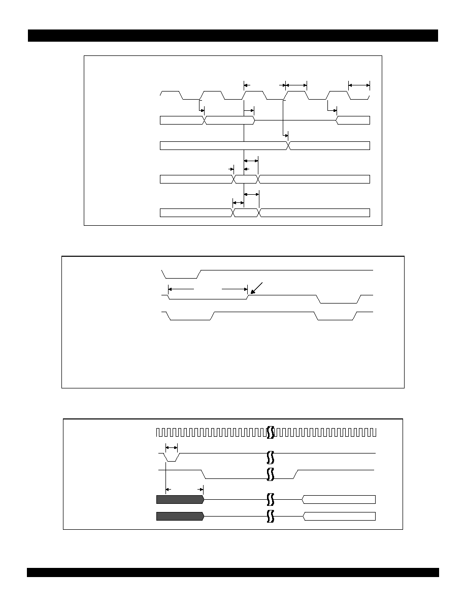
30 of 59
May 25, 2004
IDT 79RC32438
Figure 13 PCI AC Timing Waveform
Figure 14 PCI AC Timing Waveform -- PCI Reset in Host Mode
Figure 15 PCI AC Timing Waveform -- PCI Reset in Satellite Mode
Tdo_10c
Tzd_10b
Tdz_10b
Tdo_10b
Thld_10c
Tsu_10c
Thld_10b
Tsu_10b
Thigh_10a
Tper_10a
Tper_10a
valid
valid
PCICLK
Bussed output
Point to point output
Bussed input
Point to point input
Tlow_10a
Tpw_10d
Tpw_10d
PCI interface enabled
cold reset
warm reset
COLDRSTN
PCIRSTN (output)
RSTN
Note: During and after cold reset, PCIRSTN is tri-stated and requires a pull-down to reach a low state.
After the PCI interface is enabled in host mode, PCIRSTN will be driven either high or low depending on the
(tri-state)
reset state of the 79RC32438.
Tdz_10e
Tpw_10e
Tpw_10e
warm reset
CLKP
PCIRSTN (input)
RSTN
MDATA[15:0]
PCI bus signals

31 of 59
May 25, 2004
IDT 79RC32438
Signal
Symbol Reference
Edge
200MHz 233MHz 266MHz 300MHz
Unit Conditions
Timing
Diagram
Reference
Min
Max
Min
Max
Min
Max
Min
Max
I
2
C
1
1.
For more information, see the I
2
C-Bus specification by Philips Semiconductor.
SCL
Frequency none
0
100
0
100
0
100
0
100
kHz
100 KHz
See Figure 16.
Thigh_12a,
Tlow_12a
4.0
--
4.0
--
4.0
--
4.0
--
µs
Trise_12a
--
1000
--
1000
--
1000
--
1000
ns
Tfall_12a
--
300
--
300
--
300
--
300
ns
SDA
Tsu_12b
SCL rising
250
--
250
--
250
--
250
--
ns
Thld_12b
0
3.45
0
3.45
0
3.45
0
3.45
µs
Trise_12b
--
1000
--
1000
--
1000
--
1000
ns
Tfall_12b
--
300
--
300
--
300
--
300
ns
Start or repeated start
condition
Tsu_12c
SDA falling
4.7
--
4.7
--
4.7
--
4.7
--
µs
Thld_12c
4.0
--
4.0
--
4.0
--
4.0
--
µs
Stop condition
Tsu_12d
SDA rising
4.0
--
4.0
--
4.0
--
4.0
--
µs
Bus free time between
a stop and start condi-
tion
Tdelay_12e
4.7
--
4.7
--
4.7
--
4.7
--
µs
SCL
Frequency none
0
400
0
400
0
400
0
400
kHz
400 KHz
Thigh_12a,
Tlow_12a
0.6
--
0.6
--
0.6
--
0.6
--
µs
Trise_12a
--
300
--
300
--
300
--
300
ns
Tfall_12a
--
300
--
300
--
300
--
300
ns
SDA
Tsu_12b
SCL rising
100
--
100
--
100
--
100
--
ns
Thld_12b
0
0.9
0
0.9
0
0.9
0
0.9
µs
Trise_12b
--
300
--
300
--
300
--
300
ns
Tfall_12ba
--
300
--
300
--
300
--
300
ns
Start or repeated start
condition
Tsu_12c
SDA falling
0.6
--
0.6
--
0.6
--
0.6
--
µs
Thld_12c
0.6
--
0.6
--
0.6
--
0.6
--
µs
Stop condition
Tsu_12d
SDA rising
0.6
--
0.6
--
0.6
--
0.6
--
µs
Bus free time between
a stop and start condi-
tion
Tdelay_12e
1.3
--
1.3
--
1.3
--
1.3
--
µs
Table 11 I
2
C AC Timing Characteristics

32 of 59
May 25, 2004
IDT 79RC32438
Figure 16 I
2
C AC Timing Waveform
Figure 17 GPIO AC Timing Waveform
Signal
Symbol Reference
Edge
200MHz
233MHz
266MHz
300MHz
Unit Conditions
Timing
Diagram
Reference
Min
Max
Min
Max
Min
Max
Min
Max
GPIO
GPIO[31:0]
1
1.
GPIO signals must meet the setup and hold times if they are synchronous or the minimum pulse width if they are asynchronous.
Tpw_13b
2
2.
The values for this symbol were determined by calculation, not by testing.
None
2(ICLK)
--
2(ICLK)
--
2(ICLK)
--
2(ICLK)
--
ns
See Figure 17.
Table 12 GPIO AC Timing Characteristics
Tsu_12d
Thld_12c
Tsu_12c
Tsu_12b
Thld_12b
Thigh_12a
Thld_12c
Tlow_12a
SDA
SCL
Tdelay_12e
Tdo_13a
Tdo_13a
Tpw_13b
Tpw_13b
Thld_13a
Tsu_13a
EXTCLK
GPIO (synchronous output)
GPIO (synchronous input)
GPIO (asynchronous input)
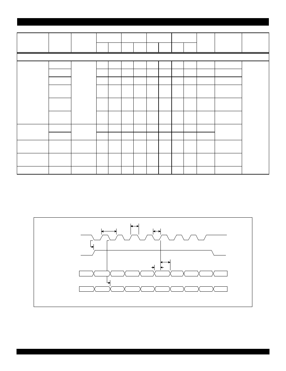
33 of 59
May 25, 2004
IDT 79RC32438
Figure 18 SPI AC Timing Waveform -- PCI Configurations Load
Signal
Symbol Reference
Edge
200MHz
233MHz
266MHz
300MHz
Unit Conditions
Timing
Diagram
Reference
Min
Max
Min
Max
Min
Max
Min
Max
SPI
1
1.
In SPI mode, the SCK period and sampling edge are programmable. In PCI mode, the SCK period is fixed and the sampling edge is rising.
SCK
Tper_15a None
--
1920
--
1920
--
1920
--
1920
ns
33 MHz PCI
See Figures 18,
19, 20 and 21.
Tper_15a
--
960
--
960
--
960
--
960
ns
66 MHz PCI
Tper_15a
100 166667 100 166667 100 166667 100 166667
ns
SPI
Thigh_15a,
Tlow_15a
930
990
930
990
930
990
930
990
ns
33 MHz PCI
Thigh_15a,
Tlow_15a
465
495
465
495
465
495
465
495
ns
66 MHz PCI
Thigh_15a,
Tlow_15a
40
83353
40
83353
40
83353
40
83353
ns
SPI
SDI
Tsu_15b
SCK rising or
falling
60
--
60
--
60
--
60
--
ns
SPI or PCI
Thld_15b
60
--
60
--
60
--
60
--
ns
SDO
Tdo_15c
SCK rising or
falling
0
60
0
60
0
60
0
60
ns
SPI or PCI
PCIEECS
2
2.
PCIEECS is the PCI serial EEPROM chip select. It is an alternate function of PCIGNTN[1].
Tdo_15d
SCK rising or
falling
0
60
0
60
0
60
0
60
ns
PCI
SCK, SDI, SDO
3
3.
In Bit I/O mode, SCK, SDI, and SDO must meet the setup and hold times if they are synchronous or the minimum pulse width if they are asynchronous.
Tpw_15e
None
2(ICLK)
--
2(ICLK)
--
2(ICLK)
--
2(ICLK)
--
ns
Bit I/O
Table 13 SPI AC Timing Characteristics
Tdo_15c
Tdo_15d
Thld_15b
Tsu_15b
Tlow_15a
Tlow_15a
Thigh_15a
Thigh_15a
Tper_15a
MSB
bit 6
bit 5
bit 4
bit 3
bit 2
bit 1
LSB
Loading PCI configuration registers through SPI from an EEPROM.
MSB
bit 6
bit 4
bit 2
LSB
bit 5
bit 3
bit 1
SCK
PCIEECS
SDI
SDO
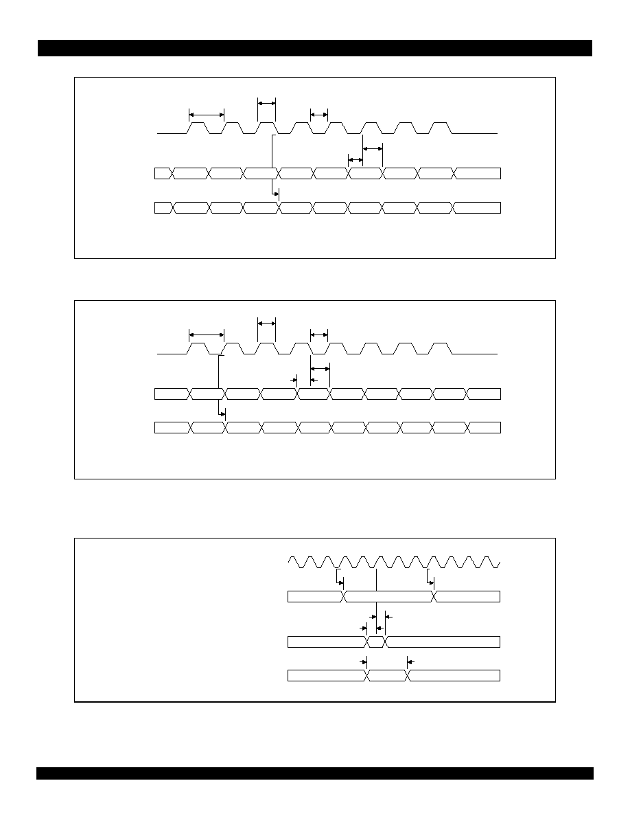
34 of 59
May 25, 2004
IDT 79RC32438
Figure 19 SPI AC Timing Waveform -- Clock Polarity 0, Clock Phase 0
Figure 20 SPI AC Timing Waveform -- Clock Polarity 0, Clock Phase 1
Figure 21 SPI AC Timing Waveform -- Bit I/O Mode
Tdo_15c
Thld_15b
Tsu_15b
Tlow_15a
Thigh_15a
Tper_15a
MSB
bit 6
bit 4
bit 5
bit 3
bit 2
bit 1
LSB
Control bits CPOL = 0, CPHA = 0 in the SPI Control Register, SPC.
MSB
bit 6
bit 4
bit 2
LSB
bit 5
bit 3
bit 1
SCK
SDI
SDO
Tdo_15c
Thld_15b
Tsu_15b
Tlow_15a
Thigh_15a
Tper_15a
MSB
bit 6
bit 4
bit 5
bit 3
bit 2
bit 1
LSB
Control bits CPOL = 0, CPHA = 1 in the SPI Control Register, SPC.
MSB
bit 6
bit 4
bit 5
bit 3
bit 1
bit 2
LSB
SCK
SDI
SDO
Tdo_15e
Tdo_15e
Tpw_15e
Tpw_15e
Thld_15e
Tsu_15e
EXTCLK
SCK, SDI, SDO (output)
SCK, SDI, SDO (input)
SCK, SDI, SDO (asynchronous input)

35 of 59
May 25, 2004
IDT 79RC32438
Signal
Symbol Reference
Edge
200MHz 233MHz 266MHz 300MHz
Unit Conditions
Timing
Diagram
Reference
Min
Max
Min
Max
Min
Max
Min
Max
EJTAG and JTAG
JTAG_TCK
Tper_16a
none
25.0
50.0
25.0
50.0
25.0
50.0
25.0
50.0
ns
See Figure 22.
Thigh_16a,
Tlow_16a
10.0
25.0
10.0
25.0
10.0
25.0
10.0
25.0
ns
JTAG_TMS
1
,
JTAG_TDI
1.
The JTAG specification, IEEE 1149.1, recommends that both JTAG_TMS and EJTAG_TMS should be held at 1 while the signal applied at JTAG_TRST_N changes from 0 to 1.
Otherwise, a race may occur if JTAG_TRST_N is deasserted (going from low to high) on a rising edge of JTAG_TCK when either JTAG_TMS or EJTAG_TMS is low, because the
TAP controller might go to either the Run-Test/Idle state or stay in the Test-Logic-Reset state.
Tsu_16b
JTAG_TCK
rising
2.4
--
2.4
--
2.4
--
2.4
--
ns
Thld_16b
1.0
--
1.0
--
1.0
--
1.0
--
ns
JTAG_TDO
Tdo_16c
JTAG_TCK
falling
--
11.3
--
11.3
--
11.3
--
11.3
ns
Tdz_16c
2
2.
The values for this symbol were determined by calculation, not by testing.
--
11.3
--
11.3
--
11.3
--
11.3
ns
JTAG_TRST_N
Tpw_16d
2
none
25.0
--
25.0
--
25.0
--
25.0
--
ns
EJTAG_TMS
1
Tsu_16e
JTAG_TCK
rising
2.0
--
2.0
--
2.0
--
2.0
--
ns
Thld_6e
1.0
--
1.0
--
1.0
--
1.0
--
ns
VSENSE
Trise_16f
none
--
2
--
2
--
2
--
2
sec
Measured from
0.5V (T
active
)
See Figure 24.
Table 14 JTAG AC Timing Characteristics

36 of 59
May 25, 2004
IDT 79RC32438
Figure 22 JTAG AC Timing Waveform
The IEEE 1149.1 specification requires that the JTAG and EJTAG TAP controllers be reset at power-up whether or not the interfaces are used for
a boundary scan or a probe. Reset can occur through a pull-down resistor on JTAG_TRST_N if the probe is not connected. However, on-chip pull-up
resistors are implemented on the RC32438 due to an IEEE 1149.1 requirement. Having on-chip pull-up and external pull-down resistors for the
JTAG_TRST_N signal requires special care in the design to ensure that a valid logical level is provided to JTAG_TRST_N, such as using a small
external pull-down resistor to ensure this level overrides the on-chip pull-up. An alternative is to use an active power-up reset circuit for
JTAG_TRST_N, which drives JTAG_TRST_N low only at power-up and then holds JTAG_TRST_N high afterwards with a pull-up resistor.
Figure 23 shows the electrical connection of the EJTAG probe target system connector.
Figure 23 Target System Electrical EJTAG Connection
Tpw_16d
Tpw_16d
Tdz_16c
Tdo_16c
Thld_16e
Tsu_16e
Thld_16b
Tsu_16b
Thld_16b
Tsu_16b
Tlow_16a
Tlow_16a
Tper_16a
Thigh_16a
JTAG_TCK
JTAG_TDI
JTAG_TMS
EJTAG_TMS
JTAG_TDO
JTAG_TRST_N
GND
1
GND
GND
GND
GND
TRST*
TDI
TDO
TMS
TCK
RST*
DINT
JTAG_TRST_N
JTAG_TDI
JTAG_TDO
EJTAG_TMS
JTAG_TCK
GND
VDD
GND
VccIO voltage
reference
Pul
l
-
u
p
Pu
ll-d
o
w
n
Series-res.
COLDRSTN
Target System
Reset Circuit
Pul
l
-
u
p
Other reset
sources
RC32438
no connect
or RSTN
VSENSE

37 of 59
May 25, 2004
IDT 79RC32438
Using the EJTAG Probe
In Figure 23, the pull-up resistors for JTAG_TDO and RST*, the pull-down resistor for JTAG_TRST_N, and the series resistor for JTAG_TDO must
be adjusted to the specific design. However, the recommended pull-up/down resistor is 1.0 k
because a low value reduces crosstalk on the cable to
the connector, allowing higher JTAG_TCK frequencies. A typical value for the series resistor is 33
. Recommended resistor values have ± 5% toler-
ance.
If a probe is used, the pull-up resistor on JTAG_TDO must ensure that the JTAG_TDO level is high when no probe is connected and the
JTAG_TDO output is tri-stated. This requirement allows reliable connection of the probe if it is hooked-up when the power is already on (hot plug). The
pull-up resistor value of around 47 k
should be sufficient. Optional diodes to protect against overshoot and undershoot voltage can be added on the
signals of the chip with EJTAG.
If a probe is used, the RST* signal must have a pull-up resistor because it is controlled by an open-collector (OC) driver in the probe, and thus is
actively pulled low only. The pull-up resistor is responsible for the high value when not driven by the probe of 25pF. The input on the target system
reset circuit must be able to accept the rise time when the pull-up resistor charges the capacitance to a high logical level. Vcc I/O must connect to a
voltage reference that drops rapidly to below 0.5V when the target system loses power, even with a capacitive load of 25pF. The probe can thus detect
the lost power condition.
For additional information on EJTAG, refer to Chapter 20 of the RC32438 User Reference Manual.
Voltage Sense Signal Timing
Figure 24 Voltage Sense Signal Timing
The target system must ensure that T
rise
is obeyed after the system reaches 0.5V (T
active
), so the probe can use this value to determine when the
target has powered-up. The probe is allowed to measure the T
rise
time from a higher value than T
active
(but lower than Vcc I/O minimum) because the
stable indication in this case comes later than the time when target power is guaranteed to be stable. If JTAG_TRST_N is asserted by a pulse at
power-up, this reset must be completed after T
rise
. If JTAG_TRST_N is asserted by a pull-down resistor, the probe will control JTAG_TRST_N. At
power-down, no power is indicated to the probe when Vcc I/O drops under the T
active
value, which the probe uses to stop driving the input signals,
except for the probe RST*.
Phase-Locked Loop (PLL)
The phase-locked loop (PLL) multiplies the external oscillator input (pin CLK) according to the parameter provided by the boot configuration vector
to create the processor clock (PCLK). Inherently, PLL circuits are only capable of generating clock frequencies within a limited range.
PLL Filters
It is recommended that the system designer provide a filter network of passive components for the PLL analog and digital power supplies.
The
PLL circuit power and PLL circuit ground should be isolated from power and ground with a filter circuit such as the one shown in Figure 25.
Because the optimum values for the filter components depend upon the application and the system noise environment, these values should be
considered as starting points for further experimentation within your specific application.
VSENSE
T
rise_16f
T
active

38 of 59
May 25, 2004
IDT 79RC32438
Figure 25 PLL Filter Circuit for Noisy Environments
Recommended Operating Supply Voltages
Recommended Operating Temperatures
Capacitive Load Deration
Refer to the
79RC32438 IBIS Model
on the IDT web site (www.idt.com).
Symbol
Parameter
Clock Speed
Minimum
Typical
Maximum
Unit
V
ss
Common ground
All speeds
0
0
0
V
V
ss
PLL
PLL ground
V
cc
I/O
I/O supply except for SSTL_2
1
1.
SSTL_2 I/Os are used to connect to DDR SDRAM.
3.0
3.3
3.6
V
V
cc
SI/O
I/O supply for SSTL_2
1
2.3
2.5
2.7
V
V
cc
PLL PLL
supply
200MHz,
233MHz
1.1
1.2
1.3
V
266MHz, 300MHz
1.2
1.3
1.4
V
V
cc
Core
Internal logic supply
200MHz, 233MHz
1.1
1.2
1.3
V
266MHz, 300MHz
1.2
1.3
1.4
V
DDRVREF
2
2.
Peak-to-peak AC noise on DDRVREF may not exceed ± 2% DDRVREF (DC).
SSTL_2 input reference
voltage
All speeds
0.5(VccSI/O)
0.5(VccSI/O)
0.5(VccSI/O)
V
V
TT
3
3.
V
TT
of the SSTL_2 transmitting device must track DDRVREF of the receiving device.
SSTL_2 termination voltage
DDRVREF - 0.04
DDRVREF
DDRVREF + 0.04
V
Table 15 RC32438 Operating Voltages
Grade
Temperature
Commercial
0
∞
C to +70
∞
C Ambient
Industrial
-40
∞
C to +85
∞
C Ambient
Table 16 RC32438 Operating Temperatures
10
µ
F
0.1
µ
F
100 pF
V
cc
V
ss
V
cc
PLL
V
ss
PLL
10 ohm
1
RC32438
V
cc
PLL
V
ss
PLL

39 of 59
May 25, 2004
IDT 79RC32438
Power-on Sequence
Three power-on sequences are given below. Sequence #1 is recommended because it will prevent I/O conflicts and will also allow the input signals
to propagate when the I/O powers are brought up.
Note: The ESD diodes may be damaged if one of the voltages is applied and one of the other voltages is at a ground level.
A. Recommended Sequence
t2 > 0 whenever possible (V
cc
Core)
t1 - t2 can be 0 (V
cc
SI/O followed by V
cc
I/O)
B. Reverse Voltage Sequence
If sequence A is not feasible, then Sequence B can be used:
t1 <50ms and t2 <50ms to prevent damage.
C. Simultaneous Power-up
VccI/O, VccSI/O, and VccCore can be powered up simultaneously.
1.2V
3.3V
2.5V
Time
t1
t2
V
cc
I/O
V
cc
SI/O
V
cc
Core
VccI/O -- 3.3V
VccSI/O -- 2.5V
VccCore (266/300MHz) -- 1.3V
VccCore (200/233MHz) -- 1.2V
Vcc1.2
Vcc3.3
Vcc2.5
Time
t1
t2
VccI/O -- 3.3V
VccSI/O -- 2.5V
VccCore (266/300MHz) -- 1.3V
VccCore (200/233MHz) -- 1.2V
VccCore
VccSI/O
VccI/O

40 of 59
May 25, 2004
IDT 79RC32438
Power Consumption
DC Electrical Characteristics
Values based on systems running at recommended supply voltages, as shown in Table 15.
Note: See Table 2, Pin Characteristics, for a complete I/O listing.
Parameter
200MHz
233MHz
266MHz
300MHz
Unit
Conditions
Typ.
Max. Typ.
Max. Typ.
Max.
Typ.
Max.
I
cc
I/O
130
150
180
200
220
250
260
300
mA
C
L
= 35 pF
T
ambient
= 25
o
C
Max. values use the maximum volt-
ages listed in Table 15. Typical values
use the typical voltages listed in that
table.
I
cc
SI/O
100
120
150
170
200
220
250
270
mA
I
cc
Core,
I
cc
PLL
Normal
mode
460
500
510
550
610
650
680
730
mA
Power
Dissipation
Normal
mode
1.2
1.6
1.6
1.9
2.0
2.4
2.4
2.7
W
Table 17 RC32438 Power Consumption
I/O Type
Para-
meter
Min.
Typical
Max.
Unit
Conditions
LOW Drive
Output
I
OL
--
14.0
--
mA
V
OL
= 0.4V
I
OH
--
-12.0
--
mA
V
OH
= 1.5V
HIGH Drive
Output
I
OL
--
24.0
--
mA
V
OL
= 0.4V
I
OH
--
-42.0
--
mA
V
OH
= 1.5V
Schmitt Trigger
Input (STI)
V
IL
-0.3
--
0.8
V
--
V
IH
2.0
--
V
cc
I/O + 0.5
V
--
SSTL_2 (for DDR
SDRAM)
I
OL
7.6
--
--
mA
V
OL
= 0.5V
I
OH
-7.6
--
--
mA
V
OH
= 1.76V
V
IL
-0.3
--
0.5(V
cc
SI/O) - 0.18
V
V
IH
0.5(V
cc
SI/O) + 0.18
--
V
cc
SI/O + 0.3
V
Table 18 DC Electrical Characteristics (Part 1 of 2)

41 of 59
May 25, 2004
IDT 79RC32438
AC Test Conditions
Figure 26 AC Test Conditions
PCI
I
OH
(AC)
Switching
-12(V
cc
I/O)
--
--
mA
0 < V
OUT
< 0.3(V
cc
I/O)
-17.1(V
cc
I/O - V
OUT
)
--
--
mA
0.3(V
cc
I/O) < V
OUT
< 0.9(V
cc
I/O)
--
--
-32(V
cc
I/O)
--
0.7(V
cc
I/O)
I
OL
(AC) Switch-
ing
+16(V
cc
I/O)
--
mA
V
cc
I/O > V
OUT
> 0.6(V
cc
I/O)
+26.7(V
OUT
)
--
mA
0.6(V
cc
I/O) > V
OUT
> 0.1(V
cc
I/O)
--
--
+38(V
cc
I/O)
mA
V
OUT
= 0.18(V
cc
I/O)
V
IL
-0.3
--
0.3(V
cc
I/O)
V
V
IH
0.5(V
cc
I/O)
--
5.5
V
Capacitance
C
IN
--
--
8.0
pF
--
Leakage
Inputs
--
--
+ 10
µ
A
Vcc (max)
I/O
LEAK
W
/
O
Pull-ups/downs
--
--
+ 10
µ
A
Vcc (max)
I/O
LEAK
with
Pull-ups/downs
--
--
+ 80
µ
A
Vcc (max)
I/O Type
Para-
meter
Min.
Typical
Max.
Unit
Conditions
Table 18 DC Electrical Characteristics (Part 2 of 2)
Input Reference Voltage
Parameter
Value
Units
SSTL I/O
Other I/O
Input pulse levels
0 to 2.5
0 to 3.3
V
Input rise/fall
0.8
1.0
ns
Input reference level
0.5(VccSI/O)
0.5(VccI/O)
V
Output reference levels
1.25
1.5
V
AC test load
35
35
pF
RC32438
Output
.
50
50
Test
Point

42 of 59
May 25, 2004
IDT 79RC32438
Absolute Maximum Ratings
Symbol
Parameter
Min
1
1.
Functional and tested operating conditions are given in Table 15. Absolute maximum ratings are stress ratings only, and func-
tional operation at the maximums is not guaranteed. Stresses beyond those listed may affect device reliability or cause perma-
nent damage to the device.
Max
1
Unit
V
CC
I/O
I/O supply except for SSTL_2
2
2.
SSTL_2 I/Os are used to connect to DDR SDRAM.
-0.6
4.0
V
V
CC
SI/O
I/O supply for SSTL_2
2
-0.6
3.0
V
V
CC
Core
Core Supply Voltage
-0.6
2.0
V
V
CC
PLL
PLL supply
-0.6
2.0
V
VinI/O
I/O Input Voltage except for SSTL_2
-0.6
V
cc
I/O+ 0.5
V
VinSI/O
I/O Input Voltage for SSTL_2
-0.6
V
cc
SI/O+ 0.5
V
T
a
Industrial
Ambient Operating Temperature
-40
+85
∞
C
T
a
Commercial
Ambient Operating Temperature
0
+70
∞
C
T
s
Storage Temperature
-40
+125
∞
C
Table 19 Absolute Maximum Ratings

43 of 59
May 25, 2004
IDT 79RC32438
Package Pin-out -- 416-PBGA Signal Pinout for RC32438
The following table lists the pin numbers, signal names, and number of alternate functions for the RC32438 device. Signal names ending with an
"_N" or "N" are active when low.
Pin
Function
Alt Pin
Function
Alt Pin
Function
Alt Pin
Function
Alt
A1
MII0CL
D11
V
ss
P1
GPIO[00]
1
AC17 V
ss
A2
GPIO[25]
1
D12
V
ss
P2
MIIMDIO
AC18 V
ss
A3
GPIO[31]
D13
V
cc
Core
P3
GPIO[02]
1
AC19 V
ss
A4
CSN[05]
D14
V
cc
Core
P4
V
cc
I/O
AC20 V
cc
I/O
A5
CSN[02]
D15
V
cc
Core
P23
V
cc
CORE
AC21 V
cc
I/O
A6
BWEN[01]
D16
V
ss
P24
DDRDM[03]
AC22 V
cc
I/O
A7
BOEN
D17
V
ss
P25
DDRDATA[31]
AC23 Vcc SI/O
A8
MDATA[15]
D18
V
ss
P26
DDRDATA[30]
AC24 Vcc SI/O
A9
MDATA[14]
D19
V
ss
R1
INST
AC25 DDROEN[00]
A10
MDATA[10]
D20
V
cc
I/O
R2
EJTAG_TMS
AC26 DDRADDR[00]
A11
MDATA[07]
D21
Vcc SI/O
R3
V
ss
AD1
JTAG_TRST_N
A12
MDATA[06]
D22
Vcc SI/O
R4
V
cc
I/O
AD2
JTAG_TMS
A13
GPIO[29]
D23
Vcc SI/O
R23
Vcc SI/O
AD3
GPIO[15]
1
A14
GPIO[22]
1
D24
Vcc SI/O
R24
DDRDATA[29]
AD4
SDA
A15
MADDR[21]
D25
DDRDATA[11]
R25
DDRADDR[13]
AD5
GPIO[27]
1
A16
MADDR[19]
D26
DDRDATA[10]
R26
DDRCSN[01]
AD6
PCIAD[30]
A17
MADDR[16]
E1
MII0TXD[02]
T1
NC
AD7
PCIAD[26]
A18
MADDR[13]
E2
MII0TXD[00]
T2
GPIO[03]
1
AD8
PCICBEN[03]
A19
MADDR[10]
E3
MII0TXD[01]
T3
CPU
AD9
PCIAD[21]
A20
MADDR[07]
E4
V
ss
T4
V
cc
I/O
AD10 PCIAD[18]
A21
MADDR[05]
E23
Vcc SI/O
T23
Vcc SI/O
AD11 PCIREQN[01]
A22
MADDR[02]
E24
DDRDATA[09]
T24
DDRCSN[00]
AD12 PCICLK
A23
RSTN E25
DDRDATA[12]
T25
DDRADDR[10]
AD13 PCIGNTN[00]
A24
DDRDATA[02]
E26
DDRDM[01]
T26
DDRADDR[12]
AD14 PCIIRDYN
A25
DDRDATA[04]
F1
MII0TXER
U1
JTAG_TDI
AD15 PCISTOPN
A26
DDRDATA[05]
F2
MII0TXD[03]
U2
JTAG_TCK
AD16 PCIPERRN
B1
MII0CRS
F3
MII0TXENP
U3
JTAG_TDO
AD17 PCIAD[15]
B2
WAITACKN
F4
V
ss
U4
V
cc
I/O
AD18 PCIAD[11]
B3
RWN
F23
Vcc SI/O
U23
V
ss
AD19 PCIAD[08]
B4
CSN[04]
F24
DDRDQS[01]
U24
DDRADDR[11]
AD20 PCIAD[06]
B5
CSN[01]
F25
DDRDATA[15]
U25
DDRWEN
AD21 PCIGNTN[03]
B6
BWEN[00]
F26
DDRDATA[14]
U26
DDRADDR[09]
AD22 PCIAD[00]
B7
BGN
G1
MII0RXER
V1
SDO
AD23 PCIAD[04]
B8
MDATA[13]
G2
MII0RXDV
V2
SDI
AD24 DDRDM[05]
Table 20 RC32438 416-pin Signal Pin-Out (Part 1 of 3)

44 of 59
May 25, 2004
IDT 79RC32438
B9
MDATA[11]
G3
MII0TXCLK
V3
GPIO[05]
1
AD25 DDROEN[02]
B10
MDATA[03]
G4
V
ss
V4
V
ss
AD26 DDROEN[01]
B11
MDATA[08]
G23
V
ss
V23
V
ss
AE1
N/C
B12
MDATA[02]
G24
DDRCKP[00]
V24
DDRADDR[08]
AE2
GPIO[13]
1
B13
GPIO[23]
1
G25
DDRDATA[16]
V25
DDRRASN
AE3
GPIO[18]
1
B14
MADDR[20]
G26
DDRDATA[13]
V26
DDRCASN
AE4
GPIO[24]
1
B15
GPIO[20]
1
H1
MII1CRS
W1
GPIO[04]
1
AE5
GPIO[26]
1
B16
MADDR[17]
H2
MII1CL
W2
SCK
AE6
PCIAD[31]
B17
MADDR[14]
H3
MII1RXCLK
W3
CLK
AE7
PCIAD[28]
B18
MADDR[12]
H4
V
ss
W4
V
ss
AE8
PCIAD[25]
B19
MADDR[09]
H23
V
ss
W23
V
ss
AE9
GPIO[30]
1
B20
MADDR[06]
H24
DDRCKN[00]
W24
DDRADDR[07]
AE10 PCIAD[22]
B21
MADDR[03]
H25
DDRDATA[18]
W25
DDRADDR[06]
AE11 PCIAD[19]
B22
MADDR[00]
H26
DDRVREF
W26
DDRBA[01]
AE12 PCIAD[16]
B23
DDRDATA[01]
J1
MII1RXD[01]
Y1
GPIO[06]
1
AE13 PCIRSTN
B24
DDRDQS[00]
J2
MII1RXD[00]
Y2
V
cc
PLL
AE14 PCIREQN[02]
B25
DDRDM[00]
J3
MII1RXD[03]
Y3
GPIO[08]
1
AE15 PCIFRAMEN
B26
DDRDATA[06]
J4
V
ss
Y4
V
ss
AE16 PCIDEVSELN
C1
MII0RXD[00]
J23
V
ss
Y23
V
ss
AE17 PCILOCKN
C2
MII0RXCLK
J24
DDRDATA[17]
Y24
DDRCKN[01]
AE18 PCICBEN[01]
C3
EXTCLK
J25
DDRDATA[21]
Y25
DDRBA[00]
AE19 PCIAD[13]
C4
COLDRSTN
J26
DDRDATA[19]
Y26
DDRADDR[05]
AE20 PCIAD[10]
C5
OEN
K1
MII1RXDV
AA1
V
ss
PLL
AE21 PCICBEN[00]
C6
CSN[03]
K2
MII1RXD[02]
AA2
GPIO[07]
1
AE22 PCIAD[05]
C7
CSN[00]
K3
MII1TXCLK
AA3
V
cc
PLL
AE23 PCIAD[02]
C8
BRN
K4
V
cc
Core
AA4
V
ss
AE24 PCIGNTN[01]
C9
BDIRN
K23
V
ss
AA23 V
ss
AE25 DDRDM[07]
C10
MDATA[12]
K24
DDRDATA[20]
AA24 DDRCKP[01]
AE26 DDRDM[04]
C11
MDATA[09]
K25
DDRDQS[02]
AA25 DDRADDR[03]
AF1
GPIO[16]
1
C12
MDATA[01]
K26
DDRCKE
AA26 DDRADDR[04]
AF2
GPIO[17]
1
C13
MDATA[05]
L1
MII1TXD[00]
AB1
GPIO[09]
1
AF3
GPIO[19]
1
C14
MDATA[04]
L2
MII1RXER
AB2
GPIO[14]
1
AF4
SCL
C15
MDATA[00]
L3
MII1TXD[03]
AB3
GPIO[11]
1
AF5
GPIO[28]
1
C16
GPIO[21]
1
L4
V
cc
Core
AB4
V
ss
AF6
PCIAD[29]
C17
MADDR[18]
L23
V
cc
Core
AB23 V
ss
AF7
PCIAD[27]
C18
MADDR[15]
L24
DDRDM[02]
AB24 V
cc
SI/O
AF8
PCIAD[24]
C19
MADDR[11]
L25
DDRDATA[24]
AB25 DDRADDR[01]
AF9
PCIAD[23]
Pin
Function
Alt Pin
Function
Alt Pin
Function
Alt Pin
Function
Alt
Table 20 RC32438 416-pin Signal Pin-Out (Part 2 of 3)

45 of 59
May 25, 2004
IDT 79RC32438
RC32438 Power Pins
C20
MADDR[08]
L26
DDRDATA[22]
AB26 DDRADDR[02]
AF10 PCIAD[20]
C21
MADDR[04]
M1
MII1TXD[02]
AC1
V
ss
PLL
AF11 PCIAD[17]
C22
MADDR[01]
M2
MII1TXD[01]
AC2
GPIO[10]
1
AF12 PCIREQN[03]
C23
DDRDATA[00]
M3
MIIMDC
AC3
GPIO[12]
1
AF13 PCIREQN[00]
C24
DDRDATA[03]
M4
V
cc
Core
AC4
V
ss
AF14 PCICBEN[02]
C25
DDRDATA[08]
M23
V
cc
Core
AC5
V
ss
AF15 PCITRDYN
C26
DDRDATA[07]
M24
DDRDATA[23]
AC6
V
ss
AF16 PCISERRN
D1
MII0RXD[03]
M25
DDRDATA[27]
AC7
V
cc
I/O
AF17 PCIPAR
D2
MII0RXD[01]
M26
DDRDATA[25]
AC8
V
cc
I/O
AF18 PCIAD[14]
D3
MII0RXD[02]
N1
MII1TXER
AC9
V
cc
I/O
AF19 PCIAD[12]
D4
V
ss
N2
MII1TXENP
AC10 V
ss
AF20 PCIAD[09]
D5
V
ss
N3
GPIO[01]
1
AC11 V
ss
AF21 PCIAD[07]
D6
V
ss
N4
V
cc
Core
AC12 V
ss
AF22 PCIAD[03]
D7
V
cc
I/O
N23
V
cc
Core
AC13 V
cc
Core
AF23 PCIAD[01]
D8
V
cc
I/O
N24
DDRDATA[26]
AC14 V
cc
Core
AF24 PCIGNTN[02]
D9
V
cc
I/O
N25
DDRDATA[28]
AC15 V
cc
Core
AF25 DDRDM[06]
D10
V
ss
N26
DDRDQS[03]
AC16 V
ss
AF26 DDROEN[03]
V
cc
I/O
V
cc
SI/O
V
cc
Core
V
cc
PLL
D7
D21
D13
Y2, AA3
D8
D22
D14
D9
D23
D15
D20
D24
K4
P4
E23
L4
R4
F23
L23
T4
R23
M4
U4
T23
M23
AC7
AB24
N4
AC8
AC23
N23
AC9
AC24
P23
AC20
AC13
AC21
AC14
AC22
AC15
Table 21 RC32438 Power Pins
Pin
Function
Alt Pin
Function
Alt Pin
Function
Alt Pin
Function
Alt
Table 20 RC32438 416-pin Signal Pin-Out (Part 3 of 3)

46 of 59
May 25, 2004
IDT 79RC32438
RC32438 Ground Pins
V
ss
V
ss
V
ss
V
ss
V
ss
PLL
D4
L10
P13
U15
AA1, AC1
D5
L11
P14
U16
D6
L12
P15
U17
D10
L13
P16
U23
D11
L14
P17
V4
D12
L15
R3
V23
D16
L16
R10
W4
D17
L17
R11
W23
D18
M10
R12
Y4
D19
M11
R13
Y23
E4
M12
R14
AA4
F4
M13
R15
AA23
G4
M14
R16
AB4
G23
M15
R17
AB23
H4
M16
T10
AC4
H23
M17
T11
AC5
J4
N10
T12
AC6
J23
N11
T13
AC10
K10
N12
T14
AC11
K11
N13
T15
AC12
K12
N14
T16
AC16
K13
N15
T17
AC17
K14
N16
U10
AC18
K15
N17
U11
AC19
K16
P10
U12
K17
P11
U13
K23
P12
U14
Table 22 RC32438 Ground Pins

47 of 59
May 25, 2004
IDT 79RC32438
RC32438 Alternate Signal Functions
RC32438 Signals Listed Alphabetically
The following table lists the RC32438 pins in alphabetical order.
Pin
GPIO
Alternate
Pin
GPIO
Alternate
Pin
GPIO
Alternate
A14
GPIO[22]
MADDR[24]
Y1
GPIO[06]
U0RTSN
AE2
GPIO[13]
U1CTSN
B13
GPIO[23]
MADDR[25]
Y3
GPIO[08]
U1SOUT
AE3
GPIO[18]
DMAFINN[0]
B15
GPIO[20]
MADDR[22]
AA2 GPIO[07]
U0CTSN
AE4
GPIO[24]
PCIREQN[4]
C16
GPIO[21]
MADDR[23]
AB1 GPIO[09]
U1SINP
AE5
GPIO[26]
PCIGNTN[4]
N3
GPIO[01]
U0SINP
AB2 GPIO[14]
DMAREQN[0]
AE9
GPIO[30]
PCIMUINTN
P1
GPIO[00]
U0SOUT
AB3 GPIO[11]
U1DSRN
AF1
GPIO[16]
DMADONE[0]
P3
GPIO[02]
U0RIN
AC2 GPIO[10]
U1DTRN
AF2
GPIO[17]
DMADONE[1]
T2
GPIO[03]
U0DCDN
AC3 GPIO[12]
U1RTSN
AF3
GPIO[19]
DMAFINN[1]
V3
GPIO[05]
U0DSRN
AD3 GPIO[15]
DMAREQN[1]
AF5
GPIO[28]
PCIGNTN[5]
W1
GPIO[04]
U0DTRN
AD5 GPIO[27]
PCIREQN[5]
Table 23 RC32438 Alternate Signal Functions
Signal Name I/O Type
Location
Signal Category
BDIRN
O
C9
Memory and Peripheral Bus
BGN
O
B7
Memory and Peripheral Bus
BOEN
O
A7
Memory and Peripheral Bus
BRN
I
C8
Memory and Peripheral Bus
BWEN[00]
O
B6
Memory and Peripheral Bus
BWEN[01]
O
A6
Memory and Peripheral Bus
CLK
I
W3
System
COLDRSTN
I
C4
System
CPU
O
T3
Debug
CSN[00]
O
C7
Memory and Peripheral Bus
CSN[01]
O
B5
CSN[02]
O
A5
CSN[03]
O
C6
CSN[04]
O
B4
CSN[05]
O
A4
Table 24 RC32438 Alphabetical Signal List (Part 1 of 9)

48 of 59
May 25, 2004
IDT 79RC32438
DDRADDR[00]
O
AC26
DDR Bus
DDRADDR[01]
O
AB25
DDRADDR[02]
O
AB26
DDRADDR[03]
O
AA25
DDRADDR[04]
O
AA26
DDRADDR[05]
O
Y26
DDRADDR[06]
O
W25
DDRADDR[07]
O
W24
DDRADDR[08]
O
V24
DDRADDR[09]
O
U26
DDRADDR[10]
O
T25
DDRADDR[11]
O
U24
DDRADDR[12]
O
T26
DDRADDR[13]
O
R25
DDRBA[00]
O
Y25
DDRBA[01]
O
W26
DDRCASN
O
V26
DDRCKE
O
K26
DDRCKN[00]
O
H24
DDRCKN[01]
O
Y24
DDRCKP[00]
O
G24
DDRCKP[01]
O
AA24
DDRCSN[00]
O
T24
DDRCSN[01]
O
R26
DDRDATA[00]
I/O
C23
DDRDATA[01]
I/O
B23
DDRDATA[02]
I/O
A24
DDRDATA[03]
I/O
C24
DDRDATA[04]
I/O
A25
DDRDATA[05]
I/O
A26
DDRDATA[06]
I/O
B26
DDRDATA[07]
I/O
C26
DDRDATA[08]
I/O
C25
DDRDATA[09]
I/O
E24
DDRDATA[10]
I/O
D26
Signal Name I/O Type
Location
Signal Category
Table 24 RC32438 Alphabetical Signal List (Part 2 of 9)

49 of 59
May 25, 2004
IDT 79RC32438
DDRDATA[11]
I/O
D25
DDR Bus
DDRDATA[12]
I/O
E25
DDRDATA[13]
I/O
G26
DDRDATA[14]
I/O
F26
DDRDATA[15]
I/O
F25
DDRDATA[16]
I/O
G25
DDRDATA[17]
I/O
J24
DDRDATA[18]
I/O
H25
DDRDATA[19]
I/O
J26
DDRDATA[20]
I/O
K24
DDRDATA[21]
I/O
J25
DDRDATA[22]
I/O
L26
DDRDATA[23]
I/O
M24
DDRDATA[24]
I/O
L25
DDRDATA[25]
I/O
M26
DDRDATA[26]
I/O
N24
DDRDATA[27]
I/O
M25
DDRDATA[28]
I/O
N25
DDRDATA[29]
I/O
R24
DDRDATA[30]
I/O
P26
DDRDATA[31]
I/O
P25
DDRDM[00]
O
B25
DDRDM[01]
O
E26
DDRDM[02]
O
L24
DDRDM[03]
O
P24
DDRDM[04]
O
AE26
DDRDM[05]
O
AD24
DDRDM[06]
O
AF25
DDRDM[07]
O
AE25
DDRDQS[00]
I/O
B24
DDRDQS[01]
I/O
F24
DDRDQS[02]
I/O
K25
DDRDQS[03]
I/O
N26
DDROEN[00]
O
AC25
DDROEN[01]
O
AD26
Signal Name I/O Type
Location
Signal Category
Table 24 RC32438 Alphabetical Signal List (Part 3 of 9)

50 of 59
May 25, 2004
IDT 79RC32438
DDROEN[02]
O
AD25
DDR Bus
DDROEN[03]
O
AF26
DDRRASN
O
V25
DDRVREF
I
H26
DDRWEN
O
U25
EJTAG_TMS
I
R2
EJTAG/ICE
EXTCLK
O
C3
System
GPIO[00]
I/O
P1
General Purpose Input/Output
GPIO[01]
I/O
N3
GPIO[02]
I/O
P3
GPIO[03]
I/O
T2
GPIO[04]
I/O
W1
GPIO[05]
I/O
V3
GPIO[06]
I/O
Y1
GPIO[07]
I/O
AA2
GPIO[08]
I/O
Y3
GPIO[09]
I/O
AB1
GPIO[10]
I/O
AC2
GPIO[11]
I/O
AB3
GPIO[12]
I/O
AC3
GPIO[13]
I/O
AE2
GPIO[14]
I/O
AB2
GPIO[15]
I/O
AD3
GPIO[16]
I/O
AF1
GPIO[17]
I/O
AF2
GPIO[18]
I/O
AE3
GPIO[19]
I/O
AF3
GPIO[20]
I/O
B15
GPIO[21]
I/O
C16
GPIO[22]
I/O
A14
GPIO[23]
I/O
B13
GPIO[24]
I/O
AE4
GPIO[25]
I/O
A2
GPIO[26]
I/O
AE5
GPIO[27]
I/O
AD5
Signal Name I/O Type
Location
Signal Category
Table 24 RC32438 Alphabetical Signal List (Part 4 of 9)

51 of 59
May 25, 2004
IDT 79RC32438
GPIO[28]
I/O
AF5
General Purpose Input/Output
GPIO[29]
I/O
A13
GPIO[30]
I/O
AE9
GPIO[31]
I/O
A3
INST
O
R1
Debug
JTAG_TCK
I
U2
EJTAG/ICE
JTAG_TDI
I
U1
JTAG_TDO
O
U3
JTAG_TMS
I
AD2
JTAG_TRST_N
I
AD1
MADDR[00]
O
B22
Memory and Peripheral Bus
MADDR[01]
O
C22
MADDR[02]
O
A22
MADDR[03]
O
B21
MADDR[04]
O
C21
MADDR[05]
O
A21
MADDR[06]
O
B20
MADDR[07]
O
A20
MADDR[08]
O
C20
MADDR[09]
O
B19
MADDR[10]
O
A19
MADDR[11]
O
C19
MADDR[12]
O
B18
MADDR[13]
O
A18
MADDR[14]
O
B17
MADDR[15]
O
C18
MADDR[16]
O
A17
MADDR[17]
O
B16
MADDR[18]
O
C17
MADDR[19]
O
A16
MADDR[20]
O
B14
MADDR[21]
O
A15
MDATA[00]
I/O
C15
MDATA[01]
I/O
C12
Signal Name I/O Type
Location
Signal Category
Table 24 RC32438 Alphabetical Signal List (Part 5 of 9)

52 of 59
May 25, 2004
IDT 79RC32438
MDATA[02]
I/O
B12
Memory and Peripheral Bus
MDATA[03]
I/O
B10
MDATA[04]
I/O
C14
MDATA[05]
I/O
C13
MDATA[06]
I/O
A12
MDATA[07]
I/O
A11
MDATA[08]
I/O
B11
MDATA[09]
I/O
C11
MDATA[10]
I/O
A10
MDATA[11]
I/O
B9
MDATA[12]
I/O
C10
MDATA[13]
I/O
B8
MDATA[14]
I/O
A9
MDATA[15]
I/O
A8
MII0CL
I
A1
Ethernet Interfaces
MII0CRS
I
B1
MII0RXCLK
I
C2
MII0RXD[00]
I
C1
MII0RXD[01]
I
D2
MII0RXD[02]
I
D3
MII0RXD[03]
I
D1
MII0RXDV
I
G2
MII0RXER
I
G1
MII0TXCLK
I
G3
MII0TXD[00]
O
E2
MII0TXD[01]
O
E3
MII0TXD[02]
O
E1
MII0TXD[03]
O
F2
MII0TXENP
O
F3
MII0TXER
O
F1
MII1CL
I
H2
MII1CRS
I
H1
MII1RXCLK
I
H3
MII1RXD[00]
I
J2
MII1RXD[01]
I
J1
Signal Name I/O Type
Location
Signal Category
Table 24 RC32438 Alphabetical Signal List (Part 6 of 9)

53 of 59
May 25, 2004
IDT 79RC32438
MII1RXD[02]
I
K2
Ethernet Interfaces
MII1RXD[03]
I
J3
MII1RXDV
I
K1
MII1RXER
I
L2
MII1TXCLK
I
K3
MII1TXD[00]
O
L1
MII1TXD[01]
O
M2
MII1TXD[02]
O
M1
MII1TXD[03]
O
L3
MII1TXENP
O
N2
MII1TXER
O
N1
MIIMDC
O
M3
MIIMDIO
I/O
P2
OEN
O
C5
Memory and Peripheral Bus
PCIAD[00]
I/O
AD22
PCI Bus
PCIAD[01]
I/O
AF23
PCIAD[02]
I/O
AE23
PCIAD[03]
I/O
AF22
PCIAD[04]
I/O
AD23
PCIAD[05]
I/O
AE22
PCIAD[06]
I/O
AD20
PCIAD[07]
I/O
AF21
PCIAD[08]
I/O
AD19
PCIAD[09]
I/O
AF20
PCIAD[10]
I/O
AE20
PCIAD[11]
I/O
AD18
PCIAD[12]
I/O
AF19
PCIAD[13]
I/O
AE19
PCIAD[14]
I/O
AF18
PCIAD[15]
I/O
AD17
PCIAD[16]
I/O
AE12
PCIAD[17]
I/O
AF11
PCIAD[18]
I/O
AD10
PCIAD[19]
I/O
AE11
PCIAD[20]
I/O
AF10
Signal Name I/O Type
Location
Signal Category
Table 24 RC32438 Alphabetical Signal List (Part 7 of 9)

54 of 59
May 25, 2004
IDT 79RC32438
PCIAD[21]
I/O
AD9
PCI Bus
PCIAD[22]
I/O
AE10
PCIAD[23]
I/O
AF9
PCIAD[24]
I/O
AF8
PCIAD[25]
I/O
AE8
PCIAD[26]
I/O
AD7
PCIAD[27]
I/O
AF7
PCIAD[28]
I/O
AE7
PCIAD[29]
I/O
AF6
PCIAD[30]
I/O
AD6
PCIAD[31]
I/O
AE6
PCICBEN[00]
I/O
AE21
PCICBEN[01]
I/O
AE18
PCICBEN[02]
I/O
AF14
PCICBEN[03]
I/O
AD8
PCICLK
I
AD12
PCIDEVSELN
I/O
AE16
PCIFRAMEN
I/O
AE15
PCIGNTN[00]
I/O
AD13
PCIGNTN[01]
I/O
AE24
PCIGNTN[02]
I/O
AF24
PCIGNTN[03]
I/O
AD21
PCIIRDYN
I/O
AD14
PCILOCKN
I/O
AE17
PCIPAR
I/O
AF17
PCIPERRN
I/O
AD16
PCIREQN[00]
I/O
AF13
PCIREQN[01]
I/O
AD11
PCIREQN[02]
I/O
AE14
PCIREQN[03]
I/O
AF12
PCIRSTN
I/O
AE13
PCISERRN
I/O
AF16
PCISTOPN
I/O
AD15
PCITRDYN
I/O
AF15
RSTN
I/O
A23
System
RWN
O
B3
Memory and Peripheral Bus
Signal Name I/O Type
Location
Signal Category
Table 24 RC32438 Alphabetical Signal List (Part 8 of 9)
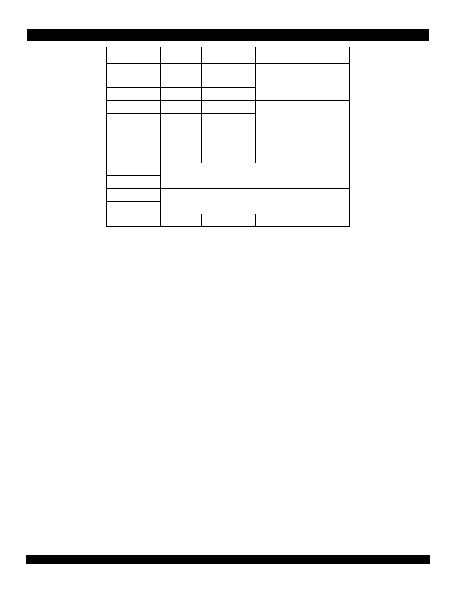
55 of 59
May 25, 2004
IDT 79RC32438
SCK
I/O
W2
SPI Interface
SCL
I/O
AF4
I
2
C
SDA
I/O
AD4
SDI
I/O
V2
SPI Interface
SDO
I/O
V1
Vcc CORE
D13, D14, D15, K4,
L4, L23, M4, M23,
N4, N23, P23,
AC13, AC14, AC15
Vcc I/O, Vcc SI/O
See Table 21 for a listing of power pins.
Vcc PLL
Vss
See Table 22 for a listing of ground pins.
Vss PLL
WAITACKN
I
B2
Memory and Peripheral Bus
Signal Name I/O Type
Location
Signal Category
Table 24 RC32438 Alphabetical Signal List (Part 9 of 9)

56 of 59
May 25, 2004
IDT 79RC32438
RC32438 Pinout -- Top View
1
2 3 4 5
6
7 8 9 10 11 12 13 14 15 16
Vss (Ground)
Vcc I/O (Power)
A
B
Vcc Core (Power)
17 18 19 20 21 22 23 24 25 26
C
D
E
F
G
H
J
K
L
M
N
P
R
T
U
V
W
Y
AA
AB
AC
AD
AE
AF
Vcc SI/O (Power)
VccPLL
VccPLL
VssPLL
VssPLL

57 of 59
May 25, 2004
IDT 79RC32438
RC32438 Package Drawing -- 416-pin BGA

58 of 59
May 25, 2004
IDT 79RC32438
RC32438 Package Drawing
--
Page Two

59 of 59
May 25, 2004
IDT 79RC32438
CORPORATE HEADQUARTERS
2975 Stender Way
Santa Clara, CA 95054
for SALES:
800-345-7015 or 408-727-6116
fax: 408-330-1748
www.idt.com
for Tech Support:
email: rischelp@idt.com
phone: 408-492-8208
Ordering Information
Valid Combinations
79RC32K438 -200BB, 233BB, 266BB, 300BB 416-pin BGA package, Commercial Temperature
79RC32K438 -200BBI, 233BBI
416-pin BGA package, Industrial Temperature
79RCXX
YY
XXXX
999
A
A
Operating
Voltage
Device
Type
Speed
Package
Temp range/
Process
K
200
Blank
Commercial Temperature
(0∞C to +70∞C Ambient)
200 MHz Pipeline Clk
1.2V +/- 0.1V Core Voltage (200/233)
Integrated Core Processor
Product
Type
79RC32
32-bit Embedded
Microprocessor
416-pin BGA
BB
233
233 MHz Pipeline Clk
438
I
Industrial Temperature
(-40∞ C to +85∞ C Ambient)
266
266 MHz Pipeline Clk
1.3V+/- 0.1V Core Voltage (266/300)
300
300 MHz Pipeline Clk