32351ds.fm

1 of 42
May 25, 2004
© 2002 Integrated Device Technology, Inc.
DSC 6053
IDT and the IDT logo are registered trademarks of Integrated Device Technology, Inc.
Features List
RC32300 32-bit Microprocessor
Enhanced MIPS-II ISA
Enhanced MIPS-IV cache prefetch instruction
DSP Instructions
MMU with 16-entry TLB
8kB Instruction cache, 2-way set associative
2kB Data cache, 2-way set associative
Per line cache locking
Write-through and write-back cache management
Debug interface through the EJTAG port
Big or little endian support
Interrupt Controller
Allows status of each interrupt to be read and masked
UARTs
Two 16550 Compatible UARTs
Baud rate support up to 1.5 Mb/s
Counter/Timers
Three general purpose 32-bit counter/timers
General Purpose I/O Pins (GPIOP)
32 individually programmable pins:
each pin programmable as input, output, or alternate function,
input can be an interrupt or NMI source,
input can also be active high or active low
4 additional, auxiliary GPIO pins can be configured as input or
output
SDRAM Controller
2 memory banks, non-interleaved, 512 MB total
32-bit wide data path
Supports 4-bit, 8-bit, and 16-bit wide SDRAM chips
SODIMM support
Stays on page between transfers
Automatic refresh generation
Peripheral Device Controller
26-bit address bus
32-bit data bus with variable width support of 8-,16-, or 32-bits
8-bit boot ROM support
6 banks available, up to 64MB per bank
Supports Flash ROM, PROM, SRAM, dual-port memory, and
peripheral devices
Supports external wait-state generation, Intel or Motorola style
Write protect capability
Direct control of optional external data transceivers
System Integrity
Programmable system watchdog timer resets system on time-
out
Programmable bus transaction times memory and peripheral
transactions and generates a warm reset on time-out
DMA
14 DMA channels
Services on-chip and external peripherals
Supports memory-to-memory, memory-to-I/O, and I/O-to-I/O
transfers
Supports flexible descriptor based operation and chaining via
linked lists of records (scatter / gather capability)
Supports unaligned transfers
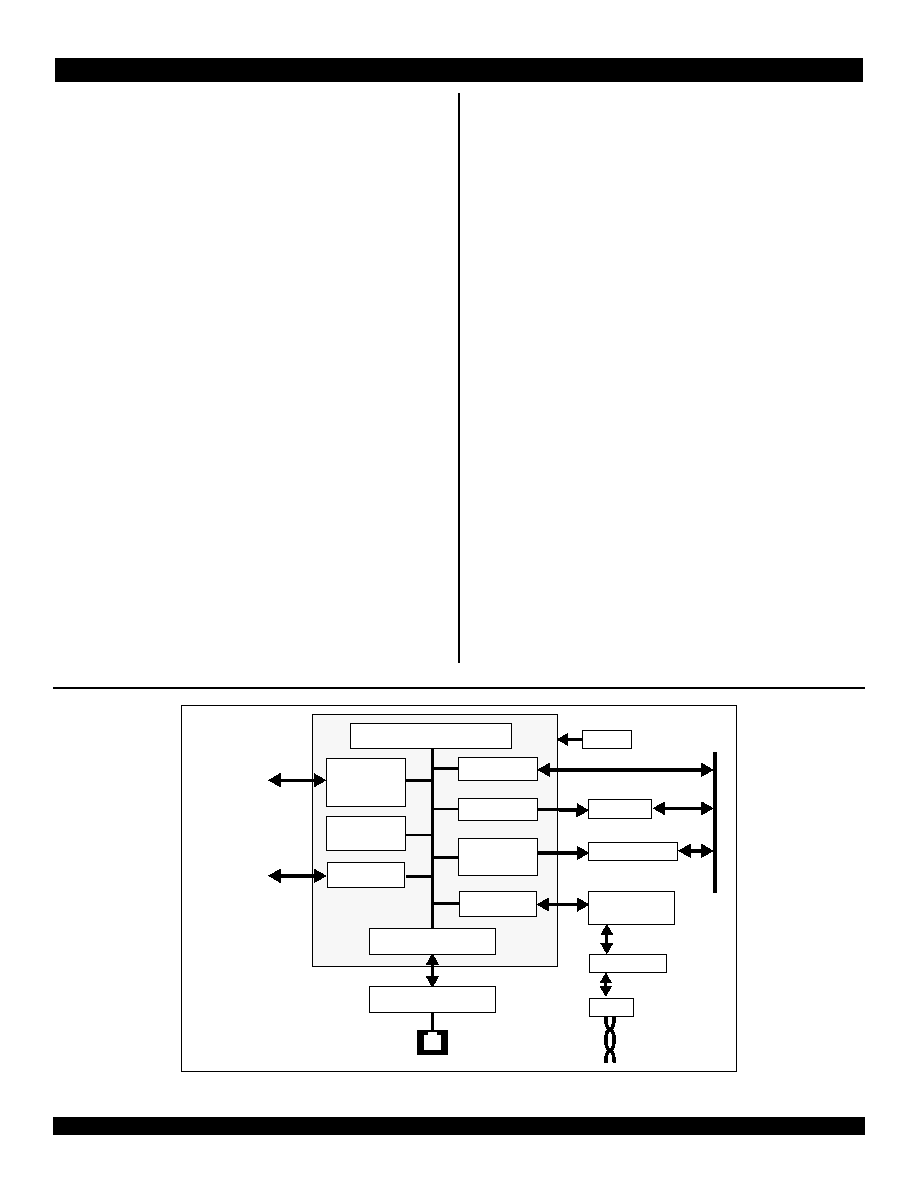
Block Diagram
EJTAG
MMU
D. Cache
I. Cache
RC32300
CPU Core
ICE
Interrupt
Controller
3 Counter
Timers
Watchdog
Timer
10/100
Ethernet
Interface
USB
Interface
16 Channel
DMA
Controller
Arbiter
Ext. Bus
Master
SDRAM &
Device
Controller
2 UARTS
(16550)
GPIO
Interface
ATM
Interface
Memory &
Peripheral Bus
Ch. 1 Ch. 2
Serial Channels
GPIO Pins
Utopia 1 / 2
:
:
79RC32351
IDT
TM
Interprise
TM
Integrated
Communications Processor
2 of 42
May 25, 2004
IDT 79RC32351
Supports burst transfers
USB
Revision 1.1 compliant
USB slave device controller
Supports a 6
th
USB endpoint
Full speed operation at 12 Mb/s
Supports control, interrupt, bulk and isochronous endpoints
Supports USB remote wakeup
Integrated USB transceiver
EJTAG
Run-time Mode provides a standard JTAG interface
Real-Time Mode provides additional pins for real-time trace
information
Ethernet
Full duplex support for 10 and 100 Mb/s Ethernet
IEEE 802.3u compatible Media Independent Interface (MII)
with serial management interface
IEEE 802.3u auto-negotiation for automatic speed selection
Flexible address filtering modes
64-entry hash table based multicast address filtering
ATM SAR
Can be configured as one UTOPIA level 1 interface or 1
UTOPIA level 2 interface with 2 address lines (3 PHYs max)
Supports 25Mb/s and faster ATM
Supports UTOPIA data path interface operation at speeds up
to 33 MHz
Supports standard 53-byte ATM cells
Performs HEC generation and checking
Cell processing discards short cells and clips long cells
16 cells worth of buffering
UTOPIA modes: 8 cell input buffer and 8 cell output buffer
Hardware support for CRC-32 generation and checking for
AAL5
Hardware support for CRC-10 generation and checking
Virtual caching receive mechanism supports reception of any
length packet without CPU intervention on up to eight simulta-
neously active receive channels
Frame Mode transmit mechanism supports transmission of
any length packet without CPU intervention
System Features
JTAG interface (IEEE Std. 1149.1 compatible)
208 pin PQFP package
2.5V core supply and 3.3V I/O supply
Up to 133 MHz pipeline frequency and up to 66 MHz bus
frequency
Figure 2 Example of xDSL Residential Gateway Using RC32351
Ethernet Transceiver
MII I/F
DMA
Channels
USB
Timers
UART
Interrupt Ctl
RC32300 CPU Core
Data Buffers
SDRAM Ctl
Memory &
I/O Controller
ATM I/F
Ethernet MAC
Ethernet to PC
Clock
SDRAM
Memory & I/O
Transmission
Convergence
Data Pump
AFE
USB to PC
Debug port
32-bit Data Bus

3 of 42
May 25, 2004
IDT 79RC32351
Device Overview
The RC32351 is a "System on a Chip" which contains a high perfor-
mance 32-bit microprocessor. The microprocessor core is used exten-
sively at the heart of the device to implement the most needed
functionalities in software with minimal hardware support. The high
performance microprocessor handles diverse general computing tasks
and specific application tasks that would have required dedicated hard-
ware. Specific application tasks implemented in software can include
routing functions, fire wall functions, modem emulation, ATM SAR
emulation, and others.
The RC32351 meets the requirements of various embedded commu-
nications and digital consumer applications. It is a single chip solution
that incorporates most of the generic system functionalities and applica-
tion specific interfaces that enable rapid time to market, very low cost
systems, simplified designs, and reduced board real estate.
CPU Execution Core
The RC32351 is built around the RC32300 32-bit high performance
microprocessor core. The RC32300 implements the enhanced MIPS-II
ISA and helps meet the real-time goals and maximize throughput of
communications and consumer systems by providing capabilities such
as a prefetch instruction, multiple DSP instructions, and cache locking.
The DSP instructions enable the RC32300 to implement 33.6 and
56kbps modem functionality in software, removing the need for external
dedicated hardware. Cache locking guarantees real-time performance
by holding critical DSP code and parameters in the cache for immediate
availability. The microprocessor also implements an on-chip MMU with a
TLB, making the it fully compliant with the requirements of real time
operating systems.
Memory and IO Controller
The RC32351 incorporates a flexible memory and peripheral device
controller providing support for SDRAM, Flash ROM, SRAM, dual-port
memory, and other I/O devices. It can interface directly to 8-bit boot
ROM for a very low cost system implementation. It enables access to
high bandwidth external memory (200 MB/sec peak) at very low system
costs. It also offers various trade-offs in cost / performance for the main
memory architecture. The timers implemented on the RC32351 satisfy
the requirements of most RTOS.
DMA Controller
The DMA controller off-loads the CPU core from moving data among
the on-chip interfaces, external peripherals, and memory. The DMA
controller supports scatter / gather DMA with no alignment restrictions,
appropriate for communications and graphics systems.
Ethernet Interface
The RC32351 contains an on-chip Ethernet MAC capable of 10 and
100 Mbps line interface with an MII interface. It supports up to 4 MAC
addresses. In a SOHO router, the high performance RC32300 CPU core
routes the data between the Ethernet and the ATM interface. In other
applications, such as high speed modems, the Ethernet interface can be
used to connect to the PC.
USB Device Interface
The RC32351 includes the industry standard USB device interface to
enable consumer appliances to directly connect to the PC.
ATM SAR
The RC32351 includes a configurable ATM SAR that supports a
UTOPIA level 1 or a UTOPIA level 2 interface. The ATM SAR is imple-
mented as a hybrid between software and hardware. A hardware block
provides the necessary low level blocks (like CRC generation and
checking and cell buffering) while the software is used for higher level
SARing functions. In xDSL modem applications, the UTOPIA port inter-
faces directly to an xDSL chip set. In SOHO routers or in a line card for a
Layer 3 switch, it provides access to an ATM network.
Enhanced JTAG Interface for ICE
For low-cost In-Circuit Emulation (ICE), the RC32300 CPU core
includes an Enhanced JTAG (EJTAG) interface. This interface consists
of two operation modes: Run-Time Mode and Real-Time Mode.
The Run-Time Mode provides a standard JTAG interface for on-chip
debugging, and the Real-Time Mode provides additional status pins--
PCST[2:0]--which are used in conjunction with the JTAG pins for real-
time trace information at the processor internal clock or any division of
the pipeline clock.

4 of 42
May 25, 2004
IDT 79RC32351
Thermal Considerations
The RC32351 consumes less than 1.5 W peak power and is guaran-
teed in an ambient temperature range of 0
° to +70° C (commercial).
Revision History
January 7, 2002: Initial publication.
May 20, 2002: Added values (in place of TBD) to Table 18, Power
Consumption.
September 19, 2002: Added COLDRSTN Trise1 parameter to Table
5, Reset and System AC Timing Characteristics.
December 6, 2002: In Features section, changed UART speed from
115 Kb/s to 1.5 Mb/s.
December 17, 2002: Added V
OH
parameter to Table 16, DC Elec-
trical Characteristics.
May 25, 2004: In Table 7, signals MIIRXCLK and MIITXCLK, the Min
and Max values for
10
Mbps Thigh1/Tlow1
were changed to 140 and
260 respectively and the Min and Max values for 100 Mbps
Thigh1/
Tlow1 were changed to 14.0 and 26.0 respectively.

5 of 42
May 25, 2004
IDT 79RC32351
Pin Description Table
The following table lists the functions of the pins provided on the RC32351. Some of the functions listed may be multiplexed onto the same pin.
To define the active polarity of a signal, a suffix will be used. Signals ending with an "N" should be interpreted as being active, or asserted, when at
a logic zero (low) level. All other signals (including clocks, buses and select lines) will be interpreted as being active, or asserted when at a logic one
(high) level.
Note: The input pads of the RC32351 do not contain internal pull-ups or pull-downs. Unused inputs should be tied off to appropriate levels.
This is especially critical for unused control signal inputs (such as BRN) which, if left floating, could adversely affect the RC32351's opera-
tion. Also, any input pin left floating can cause a slight increase in power consumption.
Name
Type I/O Type
Description
System
CLKP
I
Input
System Clock input. This is the system master clock input. The RISCore 32300 pipeline frequency is a multiple (x2, x3, or
x4) of this clock frequency. All other logic runs at this frequency or less.
COLDRSTN
I
STI
1
Cold Reset. The assertion of this signal low initiates a cold reset. This causes the RC32351 state to be initialized, boot
configuration to be loaded, and the internal processor PLL to lock onto the system clock (CLKP).
RSTN
I/O
Low Drive
with STI
Reset. This bidirectional signal is either driven low or tri-stated, an external pull-up is required to supply the high state. The
RC32351 drives RSTN low during a reset (to inform the external system that a reset is taking place) and then tri-states it.
The external system can drive RSTN low to initiate a warm reset, and then should tri-state it.
SYSCLKP
O
High Drive System clock output. This is a buffered and delayed version of the system clock input (CLKP). All SDRAM transactions
are synchronous to this clock. This pin should be externally connected to the SDRAMs and to the RC32351 SDCLKINP pin
(SDRAM clock input).
Memory and Peripheral Bus
MADDR[25:0]
O
[21:0] High
Drive
[25:22] Low
Drive with
STI
Memory Address Bus. 26-bit address bus for memory and peripheral accesses. MADDR[20:17] are used for the
SODIMM data mask enables if SODIMM mode is selected.
MADDR[22] Primary function: General Purpose I/O, GPIOP[27].
MADDR[23] Primary function: General Purpose I/O, GPIOP[28].
MADDR[24] Primary function: General Purpose I/O, GPIOP[29].
MADDR[25] Primary function: General Purpose I/O, GPIOP[30].
MDATA[31:0]
I/O
High Drive Memory Data Bus. 32-bit data bus for memory and peripheral accesses.
BDIRN
O
High Drive External Buffer Direction. External transceiver direction control for the memory and peripheral data bus, MDATA[31:0]. It
is asserted low during any read transaction, and remains high during write transactions.
BOEN[1:0]
O
High Drive External Buffer Output Enable. These signals provide two output enable controls for external data bus transceivers on
the memory and peripheral data bus, MDATA. BOEN[0] is asserted low during external device read transactions. BOEN[1]
is asserted low during SDRAM read transactions.
BRN
I
STI
External Bus Request. This signal is asserted low by an external master device to request ownership of the memory and
peripheral bus.
BGN
O
Low Drive External Bus Grant. This signal is asserted low by RC32351 to indicate that RC32351 has relinquished ownership of the
local memory and peripheral bus to an external master.
WAITACKN
I
STI
Wait or Transfer Acknowledge. When configured as wait, this signal is asserted low during a memory and peripheral
device bus transaction to extend the bus cycle. When configured as transfer acknowledge, this signal is asserted low dur-
ing a memory and peripheral device bus transaction to signal the completion of the transaction.
CSN[5:0]
O
[3:0]
High Drive
[5:4]
Low Drive
Device Chip Select. These signals are used to select an external device on the memory and peripheral bus during device
transactions. Each bit is asserted low during an access to the selected external device.
CSN[4] Primary function: General purpose I/O, GPIOP[16].
CSN[5] Primary function: General purpose I/O, GPIOP[17].
Table 1 Pin Descriptions (Part 1 of 7)
Document Outline