1 of 47
May 25, 2004
© 2004 Integrated Device Technology, Inc.
DSC 5900
IDT and the IDT logo are registered trademarks of Integrated Device Technology, Inc.
Features List
RC32300 32-bit Microprocessor
≠ Enhanced MIPS-II ISA
≠ Enhanced MIPS-IV cache prefetch instruction
≠ DSP Instructions
≠ MMU with 16-entry TLB
≠ 8KB Instruction Cache, 2-way set associative
≠ 2KB Data Cache, 2-way set associative
≠ Per line cache locking
≠ Write-through and write-back cache management
≠ Debug interface through the EJTAG port
≠ Big or Little endian support
Interrupt Controller
≠ Allows status of each interrupt to be read and masked
I
2
C
≠ Flexible I
2
C standard serial interface to connect to a variety of
peripherals
≠ Standard and fast mode timing support
≠ Configurable 7 or 10-bit addressable slave
UARTs
≠ Two 16550 Compatible UARTs
≠ Baud rate support up to 1.5 Mb/s
Counter/Timers
≠ Three general purpose 32-bit counter/timers
General Purpose I/O Pins (GPIOP)
≠ 36 individually programmable pins
≠ Each pin programmable as input, output, or alternate function
≠ Input can be an interrupt or NMI source
≠ Input can also be active high or active low
SDRAM Controller
≠ 2 memory banks, non-interleaved, 512 MB total
≠ 32-bit wide data path
≠ Supports 4-bit, 8-bit, and 16-bit wide SDRAM chips
≠ SODIMM support
≠ Stays on page between transfers
≠ Automatic refresh generation
Peripheral Device Controller
≠ 26-bit address bus
≠ 32-bit data bus with variable width support of 8-,16-, or 32-bits
≠ 8-bit boot ROM support
≠ 6 banks available, up to 64MB per bank
≠ Supports Flash ROM, PROM, SRAM, dual-port memory, and
peripheral devices
≠ Supports external wait-state generation, Intel or Motorola style
≠ Write protect capability
≠ Direct control of optional external data transceivers
System Integrity
≠ Programmable system watchdog timer resets system on time-
out
≠ Programmable bus transaction times memory and peripheral
transactions and generates a warm reset on time-out
DMA
≠ 16 DMA channels
≠ Services on-chip and external peripherals
≠ Supports memory-to-memory, memory-to-I/O, and I/O-to-I/O
transfers
≠ Supports flexible descriptor based operation and chaining via
linked lists of records (scatter / gather capability)
≠ Supports unaligned transfers
≠ Supports burst transfers
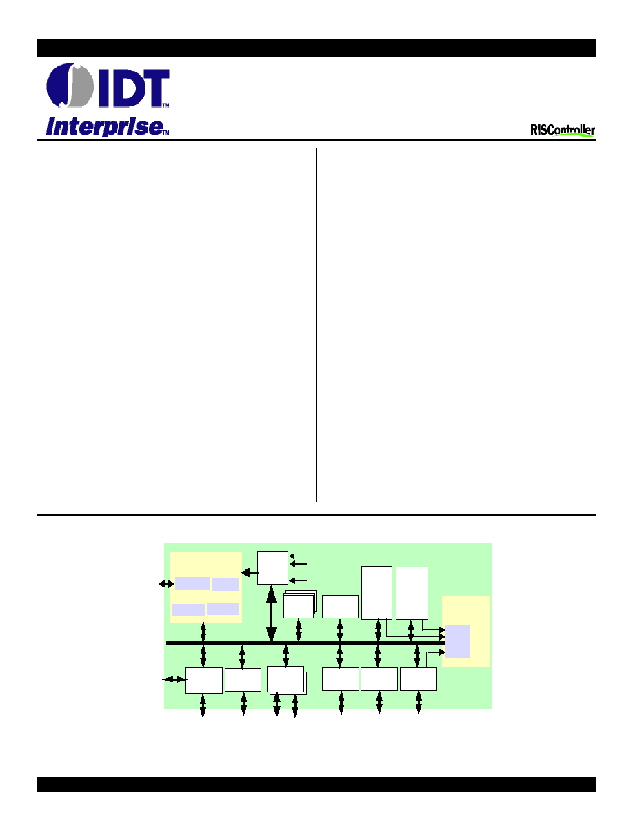
Block Diagram
Figure 1 RC32355 Internal Block Diagram
EJTAG
MMU
D. Cache
I. Cache
RC32300
CPU Core
ICE
Interrupt
Controller
3 Counter
Timers
Watchdog
Timer
10/100
Ethernet
Interface
USB
Interface
16 Channel
DMA
Controller
Arbiter
Ext. Bus
Master
SDRAM &
Device
Controller
2 UARTS
(16550)
GPIO
Interface
ATM
Interface
Memory &
Peripheral Bus
Ch. 1 Ch. 2
Serial Channels
GPIO Pins
Utopia 1 / 2
Interface
Controller
TDM
I
2
C
TDM Bus
I
2
C Bus
:
:
79RC32355
IDT
TM
Interprise
TM
Integrated
Communications Processor

2 of 47
May 25, 2004
IDT 79RC32355
USB
≠ Revision 1.1 compliant
≠ USB slave device controller
≠ Supports a 6
th
USB endpoint
≠ Full speed operation at 12 Mb/s
≠ Supports control, interrupt, bulk and isochronous endpoints
≠ Supports USB remote wakeup
≠ Integrated USB transceiver
TDM
≠ Serial Time Division Multiplexed (TDM) voice and data inter-
face
≠ Provides interface to telephone CODECs and DSPs
≠ Interface to high quality audio A/Ds and D/As with external
glue logic
≠ Support 1 to 128 8-bit time slots
≠ Compatible with Lucent CHI, GCI, Mitel ST-bus, K2 and SLD
busses
≠ Supports data rates of up to 8.192 Mb/s
≠ Supports internal or external frame generation
≠ Supports multiple non-contiguous active input and output time
slots
EJTAG
≠ Run-time Mode provides a standard JTAG interface
≠ Real-Time Mode provides additional pins for real-time trace
information
Ethernet
≠ Full duplex support for 10 and 100 Mb/s Ethernet
≠ IEEE 802.3u compatible Media Independent Interface (MII)
with serial management interface
≠ IEEE 802.3u auto-negotiation for automatic speed selection
≠ Flexible address filtering modes
≠ 64-entry hash table based multicast address filtering
ATM SAR
≠ Can be configured as one UTOPIA level 1 interface or 1
UTOPIA level 2 interface with 2 address lines (3 PHYs max)
≠ Supports 25Mb/s and faster ATM
≠ Supports UTOPIA data path interface operation at speeds up
to 33 MHz
≠ Supports standard 53-byte ATM cells
≠ Performs HEC generation and checking
≠ Cell processing discards short cells and clips long cells
≠ 16 cells worth of buffering
≠ UTOPIA modes: 8 cell input buffer and 8 cell output buffer
≠ Hardware support for CRC-32 generation and checking for
AAL5
≠ Hardware support for CRC-10 generation and checking
≠ Virtual caching receive mechanism supports reception of any
length packet without CPU intervention on up to eight simulta-
neously active receive channels
≠ Frame Mode transmit mechanism supports transmission of
any length packet without CPU intervention
System Features
≠ JTAG Interface (IEEE Std. 1149.1 compatible)
≠ 208 pin PQFP package
≠ 2.5V core supply and 3.3V I/O supply
≠ Up to 180 MHz pipeline frequency and up to 75 MHz bus
frequency
Figure 2 Example of xDSL Residential Gateway Using RC32355
SLIC
Codec
Echo
POTS telephone
RJ11
Ethernet Transceiver
MII I/F
DMA
Channels
USB
TDM
Timers
UART
Interrupt Ctl
RC32300 CPU Core
Data Buffers
SDRAM Ctl
Memory &
I/O Controller
ATM I/F
Ethernet MAC
Ethernet to PC
Clock
SDRAM
Memory & I/O
Transmission
Convergence
Data Pump
AFE
USB to PC
Debug port
32-bit Data Bus

3 of 47
May 25, 2004
IDT 79RC32355
Device Overview
The RC32355 is a "System on a Chip" which contains a high perfor-
mance 32-bit microprocessor. The microprocessor core is used exten-
sively at the heart of the device to implement the most needed
functionalities in software with minimal hardware support. The high
performance microprocessor handles diverse general computing tasks
and specific application tasks that would have required dedicated hard-
ware. Specific application tasks implemented in software can include
routing functions, fire wall functions, modem emulation, ATM SAR
emulation, and others.
The RC32355 meets the requirements of various embedded commu-
nications and digital consumer applications. It is a single chip solution
that incorporates most of the generic system functionalities and applica-
tion specific interfaces that enable rapid time to market, very low cost
systems, simplified designs, and reduced board real estate.
CPU Execution Core
The RC32355 is built around the RC32300 32-bit high performance
microprocessor core. The RC32300 implements the enhanced MIPS-II
ISA and helps meet the real-time goals and maximize throughput of
communications and consumer systems by providing capabilities such
as a prefetch instruction, multiple DSP instructions, and cache locking.
The DSP instructions enable the RC32300 to implement 33.6 and
56kbps modem functionality in software, removing the need for external
dedicated hardware. Cache locking guarantees real-time performance
by holding critical DSP code and parameters in the cache for immediate
availability. The microprocessor also implements an on-chip MMU with a
TLB, making the it fully compliant with the requirements of real time
operating systems.
Memory and I/O Controller
The RC32355 incorporates a flexible memory and peripheral device
controller providing support for SDRAM, Flash ROM, SRAM, dual-port
memory, and other I/O devices. It can interface directly to 8-bit boot
ROM for a very low cost system implementation. It enables access to
very high bandwidth external memory (380 MB/sec peak) at very low
system costs. It also offers various trade-offs in cost / performance for
the main memory architecture. The timers implemented on the RC32355
satisfy the requirements of most RTOS.
DMA Controller
The DMA controller off-loads the CPU core from moving data among
the on-chip interfaces, external peripherals, and memory. The DMA
controller supports scatter / gather DMA with no alignment restrictions,
appropriate for communications and graphics systems.
TDM Bus Interface
The RC32355 incorporates an industry standard TDM bus interface
to directly access external devices such as telephone CODECs and
quality audio A/Ds and D/As. This feature is critical for applications, such
as cable modems and xDSL modems, that need to carry voice along
with data to support Voice Over IP capability.
Ethernet Interface
The RC32355 contains an on-chip Ethernet MAC capable of 10 and
100 Mbps line interface with an MII interface. It supports up to 4 MAC
addresses. In a SOHO router, the high performance RC32300 CPU core
routes the data between the Ethernet and the ATM interface. In other
applications, such as high speed modems, the Ethernet interface can be
used to connect to the PC.
USB Device Interface
The RC32355 includes the industry standard USB device interface to
enable consumer appliances to directly connect to the PC.
ATM SAR
The RC32355 includes a configurable ATM SAR that supports a
UTOPIA level 1 or a UTOPIA level 2 interface. The ATM SAR is imple-
mented as a hybrid between software and hardware. A hardware block
provides the necessary low level blocks (like CRC generation and
checking and cell buffering) while the software is used for higher level
SARing functions. In xDSL modem applications, the UTOPIA port inter-
faces directly to an xDSL chip set. In SOHO routers or in a line card for a
Layer 3 switch, it provides access to an ATM network.
Enhanced JTAG Interface for ICE
For low-cost In-Circuit Emulation (ICE), the RC32300 CPU core
includes an Enhanced JTAG (EJTAG) interface. This interface consists
of two operation modes: Run-Time Mode and Real-Time Mode.
The Run-Time Mode provides a standard JTAG interface for on-chip
debugging, and the Real-Time Mode provides additional status pins--
PCST[2:0]--which are used in conjunction with the JTAG pins for real-
time trace information at the processor internal clock or any division of
the pipeline clock.

4 of 47
May 25, 2004
IDT 79RC32355
Thermal Considerations
The RC32355 consumes less than 2.5 W peak power. It is guaran-
teed in a ambient temperature range of 0
∞ to +70∞ C for commercial
temperature devices and - 40
∞ to +85∞ for industrial temperature
devices.
Revision History
March 29, 2001: Initial publication.
September 24, 2001: Removed references to DPI interface.
Removed references to "edge-triggered interrupt input" for GPIO pins.
Changed 208-pin package designation from DP to DH.
October 10, 2001: Revised AC timing characteristics in Tables 5, 6,
7, 8, 10, 12, and 15. Revised values in Table 18, "DC Electrical Charac-
teristics"; Table 20, "RC32355 Power Consumption"; and Figure 23,
"Typical Power Usage." Changed data sheet from Preliminary to Final.
October 23, 2001: Revised Figure 23, "Typical Power Usage."
November 1, 2001: Added Input Voltage Undershoot parameter and
a footnote to Table 21.
January 30, 2002: In Table 6, changed values from 1.5 to 1.2 for the
following signals: MDATA Tdo1, MADDR Tdo2, CASN Tdo3, CKENP
Tdo4, BDIRN Tdo5, BOEN Tdo6.
May 20, 2002: Changed values in Table 20, Power Consumption.
September 19, 2002: Added COLDRSTN Trise1 parameter to Table
5, Reset and System AC Timing Characteristics.
December 6, 2002: In Features section, changed UART speed from
115 Kb/s to 1.5 Mb/s.
December 17, 2002: Added V
OH
parameter to Table 18, DC Elec-
trical Characteristics.
January 27, 2004: Added 180MHz speed grade.
May 25, 2004: In Table 7, signals MIIRXCLK and MIITXCLK, the Min
and Max values for
10
Mbps Thigh1/Tlow1
were changed to 140 and
260 respectively and the Min and Max values for 100 Mbps
Thigh1/
Tlow1 were changed to 14.0 and 26.0 respectively.

5 of 47
May 25, 2004
IDT 79RC32355
Pin Description Table
The following table lists the functions of the pins provided on the RC32355. Some of the functions listed may be multiplexed onto the same pin.
To define the active polarity of a signal, a suffix will be used. Signals ending with an "N" should be interpreted as being active, or asserted, when at
a logic zero (low) level. All other signals (including clocks, buses and select lines) will be interpreted as being active, or asserted when at a logic one
(high) level.
Note: The input pads of the RC32355 do not contain internal pull-ups or pull-downs. Unused inputs should be tied off to appropriate levels.
This is especially critical for unused control signal inputs (such as BRN) which, if left floating, could adversely affect the RC32355's opera-
tion. Also, any input pin left floating can cause a slight increase in power consumption.
Name
Type I/O Type
Description
System
CLKP
I
Input
System Clock input. This is the system master clock input. The RISCore 32300 pipeline frequency is a multiple (x2, x3, or
x4) of this clock frequency. All other logic runs at this frequency or less.
COLDRSTN
I
STI
1
Cold Reset. The assertion of this signal low initiates a cold reset. This causes the RC32355 state to be initialized, boot
configuration to be loaded, and the internal processor PLL to lock onto the system clock (CLKP).
RSTN
I/O
Low Drive
with STI
Reset. This bidirectional signal is either driven low or tri-stated, an external pull-up is required to supply the high state. The
RC32355 drives RSTN low during a reset (to inform the external system that a reset is taking place) and then tri-states it.
The external system can drive RSTN low to initiate a warm reset, and then should tri-state it.
SYSCLKP
O
High Drive System clock output. This is a buffered and delayed version of the system clock input (CLKP). All SDRAM transactions
are synchronous to this clock. This pin should be externally connected to the SDRAMs and to the RC32355 SDCLKINP pin
(SDRAM clock input).
Memory and Peripheral Bus
MADDR[25:0]
O
[21:0] High
Drive
[25:22] Low
Drive with
STI
Memory Address Bus. 26-bit address bus for memory and peripheral accesses. MADDR[20:17] are used for the
SODIMM data mask enables if SODIMM mode is selected.
MADDR[22] Primary function: General Purpose I/O, GPIOP[27].
MADDR[23] Primary function: General Purpose I/O, GPIOP[28].
MADDR[24] Primary function: General Purpose I/O, GPIOP[29].
MADDR[25] Primary function: General Purpose I/O, GPIOP[30].
MDATA[31:0]
I/O
High Drive Memory Data Bus. 32-bit data bus for memory and peripheral accesses.
BDIRN
O
High Drive External Buffer Direction. External transceiver direction control for the memory and peripheral data bus, MDATA[31:0]. It
is asserted low during any read transaction, and remains high during write transactions.
BOEN[1:0]
O
High Drive External Buffer Output Enable. These signals provide two output enable controls for external data bus transceivers on
the memory and peripheral data bus, MDATA. BOEN[0] is asserted low during external device read transactions. BOEN[1]
is asserted low during SDRAM read transactions.
BRN
I
STI
External Bus Request. This signal is asserted low by an external master device to request ownership of the memory and
peripheral bus.
BGN
O
Low Drive External Bus Grant. This signal is asserted low by RC32355 to indicate that RC32355 has relinquished ownership of the
local memory and peripheral bus to an external master.
WAITACKN
I
STI
Wait or Transfer Acknowledge. When configured as wait, this signal is asserted low during a memory and peripheral
device bus transaction to extend the bus cycle. When configured as transfer acknowledge, this signal is asserted low dur-
ing a memory and peripheral device bus transaction to signal the completion of the transaction.
CSN[5:0]
O
[3:0]
High Drive
[5:4]
Low Drive
Device Chip Select. These signals are used to select an external device on the memory and peripheral bus during device
transactions. Each bit is asserted low during an access to the selected external device.
CSN[4] Primary function: General purpose I/O, GPIOP[16].
CSN[5] Primary function: General purpose I/O, GPIOP[17].
Table 1 Pin Descriptions (Part 1 of 8)

6 of 47
May 25, 2004
IDT 79RC32355
RWN
O
High Drive Read or Write. This signal indicates if the transaction on the memory and peripheral bus is a read transaction or a write
transaction. A high level indicates a read from an external device, a low level indicates a write to an external device.
OEN
O
High Drive Output Enable. This signal is asserted low when data should be driven by an external device during device read transac-
tions on the memory and peripheral bus.
BWEN[3:0]
O
High Drive SDRAM Byte Enable Mask or Memory and I/O Byte Write Enables. These signals are used as data input/output masks
during SDRAM transactions and as byte write enable signals during device controller transactions on the memory and
peripheral bus. They are active low.
BWEN[0] corresponds to byte lane MDATA[7:0].
BWEN[1] corresponds to byte lane MDATA[15:8].
BWEN[2] corresponds to byte lane MDATA[23:16].
BWEN[3] corresponds to byte lane MDATA[31:24].
SDCSN[1:0]
O
High Drive SDRAM Chip Select. These signals are used to select the SDRAM device on the memory and peripheral bus. Each bit is
asserted low during an access to the selected SDRAM.
RASN
O
High Drive SDRAM Row Address Strobe. The row address strobe asserted low during memory and peripheral bus SDRAM transac-
tions.
CASN
O
High Drive SDRAM Column Address Strobe. The column address strobe asserted low during memory and peripheral bus SDRAM
transactions.
SDWEN
O
High Drive SDRAM Write Enable. Asserted low during memory and peripheral bus SDRAM write transactions.
CKENP
O
Low Drive SDRAM Clock Enable. Asserted high during active SDRAM clock cycles.
Primary function: General Purpose I/O, GPIOP[21].
SDCLKINP
I
STI
SDRAM Clock Input. This clock input is a delayed version of SYSCLKP. SDRAM read data is sampled into the RC32355
on the rising edge of this clock.
ATM Interface
ATMINP[11:0]
I
STI
ATM PHY Inputs. These pins are the inputs for the ATM interface.
ATMIOP[1:0]
I/O
Low Drive
with STI
ATM PHY Bidirectional Signals. These pins are the bidirectional pins for the ATM interface.
ATMOUTP[9:0]
O
Low Drive ATM PHY Outputs. These pins are the outputs for the ATM interface.
TXADDR[1:0]
O
Low Drive ATM Transmit Address [1:0]. 2-bit address bus used for transmission in Utopia-2 mode.
TXADDR[0] Primary function: General purpose I/O, GPIOP[22].
TXADDR[1] Primary function: General purpose I/O, GPIOP[23].
RXADDR[1:0]
O
Low Drive ATM Receive Address [1:0]. 2-bit address bus for receiving in Utopia-2 mode.
RXADDR[0] Primary function: General purpose I/O, GPIOP[24].
RXADDR[1] Primary function: General purpose I/O, GPIOP[25].
TDM Bus
TDMDOP
O
High Drive TDM Serial Data Output. Serial data is driven by the RC32355 on this signal during an active output time slot. During inac-
tive time slots this signal is tri-stated.
Primary function: General purpose I/O, GPIOP[32].
TDMDIP
I
STI
TDM Serial Data Input. Serial data is received by the RC32355 on this signal during active input time slots.
Primary function: General purpose I/O, GPIOP[33].
TDMFP
I/O
High Drive TDM Frame Signal. A transition on this signal, the active polarity of which is programmable, delineates the start of a new
TDM bus frame. TDMFP is driven if the RC32355 is a master, and is received if it is a slave.
Primary function: General purpose I/O, GPIOP[34].
TDMCLKP
I
STI
TDM Clock. This input clock controls the rate at which data is sent and received on the TDM bus.
Primary function: General purpose I/O, GPIOP[35].
Name
Type I/O Type
Description
Table 1 Pin Descriptions (Part 2 of 8)

7 of 47
May 25, 2004
IDT 79RC32355
TDMTEN
O
Low Drive TDM External Buffer Enable. This signal controls an external tri-state buffer output enable connected to the TDM output
data, TDMDOP. It is asserted low when the RC32355 is driving data on TDMDOP.
Primary function: General Purpose I/O, GPIOP[26]
General Purpose Input/Output
GPIOP[0]
I/O
Low Drive
with STI
General Purpose I/O. This pin can be configured as a general purpose I/O pin.
Alternate function: UART channel 0 serial output, U0SOUTP.
GPIOP[1]
I/O
Low Drive
with STI
General Purpose I/O. This pin can be configured as a general purpose I/O pin.
Alternate function: UART channel 0 serial input, U0SINP.
GPIOP[2]
I/O
Low Drive
with STI
General Purpose I/O. This pin can be configured as a general purpose I/O pin.
1st Alternate function: UART channel 0 ring indicator, U0RIN.
2nd Alternate function: JTAG boundary scan tap controller reset, JTAG_TRST_N.
GPIOP[3]
I/O
Low Drive
with STI
General Purpose I/O. This pin can be configured as a general purpose I/O pin.
Alternate function: UART channel 0 data carrier detect, U0DCRN.
GPIOP[4]
I/O
Low Drive
with STI
General Purpose I/O. This pin can be configured as a general purpose I/O pin.
1st Alternate function: UART channel 0 data terminal ready, U0DTRN.
2nd Alternate function: CPU or DMA transaction indicator, CPUP.
GPIOP[5]
I/O
Low Drive
with STI
General Purpose I/O. This pin can be configured as a general purpose I/O pin.
Alternate function: UART channel 0 data set ready, U0DSRN.
GPIOP[6]
I/O
Low Drive
with STI
General Purpose I/O. This pin can be configured as a general purpose I/O pin.
Alternate function: UART channel 0 request to send, U0RTSN.
GPIOP[7]
I/O
Low Drive
with STI
General Purpose I/O.
This pin can be configured as a general purpose I/O pin.
Alternate function: UART channel 0 clear to send, U0CTSN.
GPIOP[8]
I/O
Low Drive
with STI
General Purpose I/O. This pin can be configured as a general purpose I/O pin.
1st Alternate function: UART channel 1 serial output, U1SOUTP.
2nd Alternate function: Active DMA channel code, DMAP[3].
GPIOP[9]
I/O
Low Drive
with STI
General Purpose I/O. This pin can be configured as a general purpose I/O pin.
1st Alternate function: UART channel 1 serial input, U1SINP.
2nd Alternate function: Active DMA channel code, DMAP[2].
GPIOP[10]
I/O
Low Drive
with STI
General Purpose I/O. This pin can be configured as a general purpose I/O pin.
1st Alternate function: UART channel 1 data terminal ready, U1DTRN.
2nd Alternate function: ICE PC trace status, EJTAG_PCST[0].
GPIOP[11]
I/O
Low Drive
with STI
General Purpose I/O. This pin can be configured as a general purpose I/O pin.
1st Alternate function: UART channel 1 data set ready, U1DSRN.
2nd Alternate function: ICE PC trace status, EJTAG_PCST[1].
GPIOP[12]
I/O
Low Drive
with STI
General Purpose I/O. This pin can be configured as a general purpose I/O pin.
1st Alternate function: UART channel 1 request to send, U1RTSN.
2nd Alternate function: ICE PC trace status, EJTAG_PCST[2].
GPIOP[13]
I/O
Low Drive
with STI
General Purpose I/O. This pin can be configured as a general purpose I/O pin.
1st Alternate function: UART channel 1 clear to send, U1CTSN.
2nd Alternate function: ICE PC trace clock, EJTAG_DCLK.
GPIOP[14]
I/O
Low Drive
with STI
General Purpose I/O. This pin can be configured as a general purpose I/O pin.
Alternate function: I
2
C interface data, SDAP.
GPIOP[15]
I/O
Low Drive
with STI
General Purpose I/O. This pin can be configured as a general purpose I/O pin.
Alternate function: I
2
C interface clock, SCLP.
GPIOP[16]
I/O
High Drive General Purpose I/O. This pin can be configured as a general purpose I/O pin.
Alternate function: Memory and peripheral bus chip select, CSN[4].
Name
Type I/O Type
Description
Table 1 Pin Descriptions (Part 3 of 8)

8 of 47
May 25, 2004
IDT 79RC32355
GPIOP[17]
I/O
High Drive General Purpose I/O. This pin can be configured as a general purpose I/O pin.
Alternate function: Memory and peripheral bus chip select, CSN[5].
GPIOP[18]
I/O
Low Drive
with STI
General Purpose I/O. This pin can be configured as a general purpose I/O pin.
Alternate function: External DMA device request, DMAREQN.
GPIOP[19]
I/O
Low Drive
with STI
General Purpose I/O. This pin can be configured as a general purpose I/O pin.
Alternate function: External DMA device done, DMADONEN.
GPIOP[20]
I/O
Low Drive
with STI
General Purpose I/O. This pin can be configured as a general purpose I/O pin.
Alternate function: USB start of frame, USBSOF.
GPIOP[21]
I/O
Low Drive
with STI
General Purpose I/O. This pin can be configured as a general purpose I/O pin.
Alternate function: SDRAM clock enable CKENP.
GPIOP[22]
I/O
Low Drive
with STI
General Purpose I/O. This pin can be configured as a general purpose I/O pin.
Alternate function: ATM transmit PHY address, TXADDR[0].
GPIOP[23]
I/O
Low Drive
with STI
General Purpose I/O. This pin can be configured as a general purpose I/O pin.
1st Alternate function: ATM transmit PHY address, TXADDR[1].
2nd Alternate function: Active DMA channel code, DMAP[0].
GPIOP[24]
I/O
Low Drive
with STI
General Purpose I/O. This pin can be configured as a general purpose I/O pin.
Alternate function: ATM receive PHY address, RXADDR[0].
GPIOP[25]
I/O
Low Drive
with STI
General Purpose I/O. This pin can be configured as a general purpose I/O pin.
1st Alternate function: ATM receive PHY address, RXADDR[1].
2nd Alternate function: Active DMA channel code, DMAP[1].
GPIOP[26]
I/O
Low Drive
with STI
General Purpose I/O. This pin can be configured as a general purpose I/O pin.
Alternate function: TDM external buffer enable, TDMTEN.
GPIOP[27]
I/O
Low Drive
with STI
General Purpose I/O. This pin can be configured as a general purpose I/O pin.
Alternate function: Memory and peripheral bus address, MADDR[22].
GPIOP[28]
I/O
Low Drive
with STI
General Purpose I/O. This pin can be configured as a general purpose I/O pin.
Alternate function: Memory and peripheral bus address, MADDR[23].
GPIOP[29]
I/O
Low Drive
with STI
General Purpose I/O. This pin can be configured as a general purpose I/O pin.
Alternate function: Memory and peripheral bus address, MADDR[24].
GPIOP[30]
I/O
Low Drive
with STI
General Purpose I/O. This pin can be configured as a general purpose I/O pin.
Alternate function: Memory and peripheral bus address, MADDR[25].
GPIOP[31]
I/O
Low Drive
with STI
General Purpose I/O. This pin can be configured as a general purpose I/O pin.
1ST Alternate function: DMA finished, DMAFIN.
2nd Alternate function: EJTAG/ICE reset, EJTAG_TRST_N.
GPIOP[32]
I/O
High Drive General Purpose I/O. This pin can be configured as a general purpose I/O pin.
Alternate function: TDM interface data output, TDMDOP. At reset, this pin defaults to the primary function, GPIOP[32].
GPIOP[33]
I/O
Low Drive
with STI
General Purpose I/O. This pin can be configured as a general purpose I/O pin.
Alternate function: TDM interface data input, TDMDIP. At reset, this pin defaults to the primary function, GPIOP[33].
GPIOP[34]
I/O
High Drive General Purpose I/O. This pin can be configured as a general purpose I/O pin.
Alternate function: TDM interface frame signal, TDMFP. At reset, this pin defaults to the primary function, GPIOP[34].
GPIOP[35]
I/O
Low Drive
with STI
General Purpose I/O. This pin can be configured as a general purpose I/O pin.
Alternate function: TDM interface clock, TDMCLKP. At reset, this pin defaults to the primary function, GPIOP[35].
DMA
DMAFIN
O
Low
External DMA finished. This signal is asserted low by the RC32355 when the number of bytes specified in the DMA
descriptor have been transferred to or from an external device.
Primary function: General Purpose I/O, GPIOP[31]. At reset, this pin defaults to primary function GPIOP[31].
2nd Alternate function: EJTAG_TRST_N.
Name
Type I/O Type
Description
Table 1 Pin Descriptions (Part 4 of 8)

9 of 47
May 25, 2004
IDT 79RC32355
DMAREQN
I
STI
External DMA Device Request. The external DMA device asserts this pin low to request DMA service.
Primary function: General purpose I/O, GPIOP[18]. At reset, this pin defaults to primary function GPIOP[18].
DMADONEN
I
STI
External DMA Device Done. The external DMA device asserts this signal low to inform the RC32355 that it is done with
the current DMA transaction.
Primary function: General purpose I/O, GPIOP[19]. At reset, this pin defaults to primary function GPIOP[19].
USB
USBCLKP
I
STI
USB Clock. 48 MHz clock input used as time base for the USB interface.
USBDN
I/O
USB
USB D- Data Line. This is the negative differential USB data signal.
USBDP
I/O
USB
USB D+ Data Line. This is the positive differential USB data signal.
USBSOF
O
Low Drive USB start of frame.
Primary function: General Purpose I/O, GPIOP[20]. At reset, this pin defaults to primary function GPIOP[20].
Ethernet
MIICOLP
I
STI
MII Collision Detected. This signal is asserted by the ethernet PHY when a collision is detected.
MIICRSP
I
STI
MII Carrier Sense. This signal is asserted by the ethernet PHY when either the transmit or receive medium is not idle.
MIIMDCP
O
Low Drive MII Management Data Clock. This signal is used as a timing reference for transmission of data on the management inter-
face.
MIIMDIOP
I/O
Low Drive
with STI
MII Management Data. This bidirectional signal is used to transfer data between the station management entity and the
ethernet PHY.
MIIRXCLKP
I
STI
MII Receive Clock. This clock is a continuous clock that provides a timing reference for the reception of data.
MIIRXDP[3:0]
I
STI
MII Receive Data. This nibble wide data bus contains the data received by the ethernet PHY.
MIIRXDVP
I
STI
MII Receive Data Valid. The assertion of this signal indicates that valid receive data is in the MII receive data bus.
MIIRXERP
I
STI
MII Receive Error. The assertion of this signal indicates that an error was detected somewhere in the ethernet frame cur-
rently being sent in the MII receive data bus.
MIITXCLKP
I
STI
MII Transmit Clock. This clock is a continuous clock that provides a timing reference for the transfer of transmit data.
MIITXDP[3:0]
O
Low Drive MII Transmit Data. This nibble wide data bus contains the data to be transmitted.
MIITXENP
O
Low Drive MII Transmit Enable. The assertion of this signal indicates that data is present on the MII for transmission.
MIITXERP
O
Low Drive MII Transmit Coding Error. When this signal is asserted together with MIITXENP, the ethernet PHY will transmit symbols
which are not valid data or delimiters.
I
2
C
SCLP
I/O
Low Drive
with STI
I
2
C Interface Clock. An external pull-up is required on SCLP, see the I
2
C spec.
2
Primary function: General purpose I/O, GPIOP[15]. At reset, this pin defaults to primary function GPIOP[15].
SDAP
I/O
Low Drive
with STI
I
2
C Interface Data Pin. An external pull-up is required on SDAP, see the I
2
C spec.
2
Primary function: General purpose I/O, GPIOP[14]. At reset, this pin defaults to primary function GPIOP[14].
EJTAG
JTAG_TCK
I
STI
JTAG Clock. This is an input test clock, used to shift data into or out of the boundary scan logic. This signal requires an
external resistor, listed in Table 16.
JTAG_TDI
I
STI
JTAG Data Input. This is the serial data shifted into the boundary scan logic. This signal requires an external resistor,
listed in Table 16. This is also used to input EJTAG_DINTN during EJTAG/ICE mode. EJTAG_DINTN is an interrupt to
switch the PC trace mode off.
JTAG_TDO
O
Low Drive JTAG Data Output. This is the serial data shifted out from the boundary scan logic. When no data is being shifted out, this
signal is tri-stated. This signal requires an external resistor, listed in Table 16. This is also used to output the EJTAG_TPC
during EJTAG/ICE mode. EJTAG_TPC is the non-sequential program counter output.
Name
Type I/O Type
Description
Table 1 Pin Descriptions (Part 5 of 8)

10 of 47
May 25, 2004
IDT 79RC32355
JTAG_TMS
I
STI
JTAG Mode Select. This input signal is decoded by the tap controller to control test operation. This signal requires an
external resistor, listed in Table 16.
EJTAG_PCST[0]
O
Low Drive PC trace status. This bus gives the PC trace status information during EJTAG/ICE mode. EJTAG/ICE enable is selected
during reset using the boot configuration and overrides the selection of the Primary and Alternate functions. This signal
requires an external resistor, listed in Table 16.
Primary function: General Purpose I/O, GPIOP[10].
1st Alternate function: UART channel 1 data terminal ready, U1DTRN.
EJTAG_PCST[1]
O
Low Drive PC trace status. This bus gives the PC trace status information during EJTAG/ICE mode. EJTAG/ICE enable is selected
during reset using the boot configuration and overrides the selection of the Primary and Alternate functions. This signal
requires an external resistor, listed in Table 16.
Primary function: General Purpose I/O, GPIOP[11]. At reset, this pin defaults to primary function GPIOP[11].
1st Alternate function: UART channel 1 data set ready, U1DSRN.
EJTAG_PCST[2]
O
Low Drive PC trace status. This bus gives the PC trace status information during EJTAG/ICE mode. EJTAG/ICE enable is selected
during reset using the boot configuration and overrides the selection of the Primary and Alternate functions. This signal
requires an external resistor, listed in Table 16.
Primary function: General Purpose I/O, GPIOP[12].
1st Alternate function: UART channel 1 request to send, U1RTSN.
EJTAG_DCLK
O
Low Drive PC trace clock. This is used to capture address and data during EJTAG/ICE mode. EJTAG/ICE enable is selected during
reset using the boot configuration and overrides the selection of the Primary and Alternate functions. This signal requires
an external resistor, listed in Table 16.
Primary function: General Purpose I/O, GPIOP[13].
1st Alternate function: UART channel 1 clear to send, U1CTSN.
EJTAG_TRST_N
I
STI
EJTAG Test Reset. EJTAG_TRST_N is an active-low signal for asynchronous reset of only the EJTAG/ICE controller.
EJTAG_TRST_N requires an external pull-up on the board. EJTAG/ICE enable is selected during reset using the boot con-
figuration and overrides the selection of the Primary and Alternate functions. This signal requires an external resistor, listed
in Table 16.
Primary: General Purpose I/O, GPIOP[31]
1st Alternate function: DMA finished output, DMAFIN.
JTAG_TRST_N
I
STI
JTAG Test Reset. JTAG_TRST_N is an active-low signal for asynchronous reset of only the JTAG boundary scan control-
ler. JTAG_TRST_N requires an external pull-down on the board that will hold the JTAG boundary scan controller in reset
when not in use if selected. JTAG reset enable is selected during reset using the boot configuration and overrides the
selection of the Primary and Alternate functions.
Primary function: General Purpose I/O, GPIOP[2].
1st Alternate function: UART channel 0 ring indicator, U0RIN.
Debug
INSTP
O
Low Drive Instruction or Data Indicator. This signal is driven high during CPU instruction fetches and low during CPU data transac-
tions on the memory and peripheral bus.
CPUP
O
Low Drive CPU or DMA Transaction Indicator. This signal is driven high during CPU transactions and low during DMA transactions
on the memory and peripheral bus if CPU/DMA Transaction Indicator Enable is enabled. CPU/DMA Status mode enable is
selected during reset using the boot configuration and overrides the selection of the Primary and Alternate functions.
Primary function: General Purpose I/O, GPIOP[4].
1st Alternate function: UART channel 0 data terminal ready U0DTRN.
DMAP[0]
O
Low Drive Active DMA channel code. DMA debug enable is selected during reset using the boot configuration and overrides the
selection of the Primary and Alternate functions.
Primary function: General Purpose I/O, GPIOP[23].
1st Alternate function: TXADDR[1].
DMAP[1]
O
Low Drive Active DMA channel code. DMA debug enable is selected during reset using the boot configuration and overrides the
selection of the Primary and Alternate functions.
Primary function: General Purpose I/O, GPIOP[25].
1st Alternate function: RXADDR[1].
Name
Type I/O Type
Description
Table 1 Pin Descriptions (Part 6 of 8)

11 of 47
May 25, 2004
IDT 79RC32355
DMAP[2]
O
Low Drive Active DMA channel code. DMA debug enable is selected during reset using the boot configuration and overrides the
selection of the Primary and Alternate functions.
Primary function: General Purpose I/O, GPIOP[9].
1st Alternate function: U1SINP.
DMAP[3]
O
Low Drive Active DMA channel code. DMA debug enable is selected during reset using the boot configuration and overrides the
selection of the Primary and Alternate functions.
Primary function: General Purpose I/O, GPIOP[8].
1st Alternate function: U1SOUTP.
UART
U0SOUTP
I
STI
UART channel 0 serial transmit.
Primary function: General Purpose I/O, GPIOP[0]. At reset, this pin defaults to primary function GPIOP[0].
U0SINP
I
STI
UART channel 0 serial receive.
Primary function: General Purpose I/O, GPIOP[1]. At reset, this pin defaults to primary function GPIOP[1].
U0RIN
I
STI
UART channel 0 ring indicator.
Primary function: General Purpose I/O, GPIOP[2]. At reset, this pin defaults to primary function GPIOP[2] if JTAG reset
enable is not selected during reset using the boot configuration.
2nd Alternate function: JTAG boundary scan reset, JTAG_TRST_N.
U0DCRN
I
STI
UART channel 0 data carrier detect.
Primary function: General Purpose I/O, GPIOP[3]. At reset, this pin defaults to primary function GPIOP[3].
U0DTRN
O
Low Drive UART channel 0 data terminal ready.
Primary function: General Purpose I/O, GPIOP[4]. At reset, this pin defaults to primary function GPIOP[4] if CPU/DMA Sta-
tus Mode enable is not selected during reset using the boot configuration.
2nd Alternate function: CPU or DMA transaction indicator, CPUP.
U0DSRN
I
STI
UART channel 0 data set ready.
Primary function: General Purpose I/O, GPIOP[5]. At reset, this pin defaults to primary function GPIOP[5].
U0RTSN
O
Low Drive UART channel 0 request to send.
Primary function: General Purpose I/O, GPIOP[6]. At reset, this pin defaults to primary function GPIOP[6].
U0CTSN
I
STI
UART channel 0 clear to send.
Primary function: General Purpose I/O, GPIOP[7]. At reset, this pin defaults to primary function GPIOP[7].
U0SOUTP
O
Low Drive UART channel 1 serial transmit.
Primary function: General Purpose I/O, GPIOP[8]. At reset, this pin defaults to primary function GPIOP[8] if DMA Debug
enable is not selected during reset using the boot configuration.
2nd Alternate function: DMA channel, DMAP[3].
U1SINP
I
STI
UART channel 1 serial receive.
Primary function: General Purpose I/O, GPIOP[9]. At reset, this pin defaults to primary function GPIOP[9] if DMA Debug
enable is not selected during reset using the boot configuration.
2nd Alternate function: DMA channel, DMAP[2].
U1DTRN O
Low
Drive UART channel 1 data terminal ready.
Primary function: General Purpose I/O, GPIOP[10]. At reset, this pin defaults to primary function GPIOP[10] if ICE Interface
enable is not selected during reset using the boot configuration.
Alternate function: PC trace status bit 0, EJTAG_PCST[0].
U1DSRN
I
STI
UART channel 1 data set ready.
Primary function: General Purpose I/O, GPIOP[11]. At reset, this pin defaults to primary function GPIOP[11] if ICE Interface
enable is not selected during reset using the boot configuration.
2nd Alternate function: PC trace status bit 1, EJTAG_PCST[1].
U1RTSN
O
Low Drive UART channel 1 request to send.
Primary function: General Purpose I/O, GPIOP[12]. At reset, this pin defaults to primary function GPIOP[12] if ICE Interface
enable is not selected during reset using the boot configuration.
2nd Alternate function: PC trace status bit 2, EJTAG_PCST[2].
Name
Type I/O Type
Description
Table 1 Pin Descriptions (Part 7 of 8)

12 of 47
May 25, 2004
IDT 79RC32355
Boot Configuration Vector
The boot configuration vector is read into the RC32355 during cold reset. The vector defines parameters in the RC32355 that are essential to oper-
ation when cold reset is complete.
The encoding of boot configuration vector is described in Table 2, and the vector input is illustrated in Figure 6.
U1CTSN
I
STI
UART channel 1 clear to send.
Primary function: General Purpose I/O, GPIOP[13]. At reset, this pin defaults to primary function GPIOP[13] if ICE Interface
enable is not selected during reset using the boot configuration.
2nd Alternate function: PC trace clock, EJTAG_DCLK.
1.
Schmitt Trigger Input.
2. 2
I
2
C - Bus Specification by Philips Semiconductors.
Signal
Name/Description
MDATA[2:0]
Clock Multiplier. This field specifies the value by which the system clock (CLKP) is multiplied internally to generate the CPU pipeline clock.
0x0 - multiply by 2
0x1 - multiply by 3
0x2 - multiply by 4
0x3 - reserved
0x4 - reserved
0x5 - reserved
0x6 - reserved
0x7 - reserved
MDATA[3]
Endian. This bit specifies the endianness of RC32355.
0x0 - little endian
0x1 - big endian
MDATA[4]
Reserved. Must be set to 0.
MDATA[5]
Debug Boot Mode. When this bit is set, the RC32355 begins executing from address 0xFF20_0200 rather than 0xBFC0_0000 following a reset.
0x0 - regular mode (processor begins executing at 0xBFC0_0000)
0x1 - debug boot mode (processor begins executing at 0xFF20_0200)
MDATA[7:6]
Boot Device Width. This field specifies the width of the boot device.
0x0 - 8-bit boot device width
0x1 - 16-bit boot device width
0x2 - 32-bit boot device width
0x3 - reserved
MDATA[8]
EJTAG/ICE Interface Enable. When this bit is set, Alternate 2 pin functions EJTAG_PCST[2:0], EJTAG_DCLK, and EJTAG_TRST_N are
selected.
0x0 - GPIOP[31, 13:10] pins behaves as GPIOP
0x1 - GPIOP[31] pin behaves as EJTAG_TRST_N,
GPIOP[12:10] pins behave as EJTAG_PCST[2:0], and
GPIOP[13] pin behaves as EJTAG_DCLK
MDATA[9]
Fast Reset. When this bit is set, RC32355 drives RSTN for 64 clock cycles, used during test only. Clear this bit for normal operation.
0x0 - Normal reset: RC32355 drives RSTN for minimum of 4096 clock cycles
0x1 - Fast Reset: RC32355 drives RSTN for 64 clock cycles (test only)
MDATA[10]
DMA Debug Enable. When this bit is set, Alternate 2 pin function, DMAP is selected. DMAP provides the DMA channel number during memory
and peripheral bus DMA transactions.
0x0 - GPIOP[8, 9, 25, 23] pins behave as GPIOP
0x1 - GPIOP[8, 9, 25, 23] pins behave as DMAP[3:0]
Table 2 Boot Configuration Vector Encoding (Part 1 of 2)
Name
Type I/O Type
Description
Table 1 Pin Descriptions (Part 8 of 8)

13 of 47
May 25, 2004
IDT 79RC32355
MDATA[11]
Hold SYSCLKP Constant. For systems that do not require a SYSCLKP output and can instead use CLKP, setting this bit to a one causes the
SYSCLKP output to be held at a constant level. This may be used to reduce EMI.
0x0 - Allow SYSCLKP to toggle
0x1 - Hold SYSCLKP constant
MDATA[12]
JTAG Boundary Scan Reset Enable. When this bit is set, Alternate 2 pin function, JTAG_TRST_N is selected.
0x0 - GPIOP[2] pin behaves as GPIOP
0x1 - GPIOP[2] pin behaves as JTAG_TRST_N
MDATA[13]
CPU / DMA Transaction Indicator Enable. When this bit is set, Alternate 2 pin function, CPUP is selected.
0x0 - GPIOP[4] pin behaves as GPIOP
0x1 - GPIOP[4] pin behaves as CPUP
MDATA[15:14] Reserved. These pins must be driven low during boot configuration.
Signal
Name/Description
Table 2 Boot Configuration Vector Encoding (Part 2 of 2)

14 of 47
May 25, 2004
IDT 79RC32355
Logic Diagram
The following Logic Diagram shows the primary pin functions of the RC32355.
Figure 3 Logic Diagram
22
32
4
MADDR[21:0]
MDATA[31:0]
BWEN[3:0]
OEN
RWN
4
CSN[3:0]
WAITACKN
BRN
BGN
RASN
CASN
SDWEN
2
SDCSN[1:0]
2
BOEN[1:0]
BDIRN
12
2
10
ATMINP[11:0]
ATMIOP[1:0]
ATMOUTP[9:0]
32
GPIOP[31:0]
USBDP
USBDN
USBCLKP
MIIRXDP[3:0]
4
MIIRXDVP
MIIRXERP
MIIRXCLKP
MIICRSP
MIICOLP
MIITXDP[3:0]
4
MIITXENP
MIITXERP
MIITXCLKP
MIIMDCP
MIIMDIOP
JTAG_TCK
JTAG_TMS
JTAG_TDI
JTAG_TDO
CLKP
SYSCLKP
COLDRSTN
RC32355
Miscell
a
neous
Signals
USB
Interfac
e
Et
hernet
Interface
JT
AG
General Purpose
I
npu
t/
Outp
ut
AT
M
In
te
rfac
e
Me
mor
y
a
n
d
RSTN
SDCLKINP
De
bug
Logic
Diagram
Pe
riph
eral Bu
s
VccCore
VccI/O
Vss
Po
we
r
/
Gr
oun
d
VccP (PLL)
VssP (PLL)
(Primary
Functions)
INSTP
4
GPIOP[35:32]
TDM
Input/O
u
tput
G
e
neral Purpose

15 of 47
May 25, 2004
IDT 79RC32355
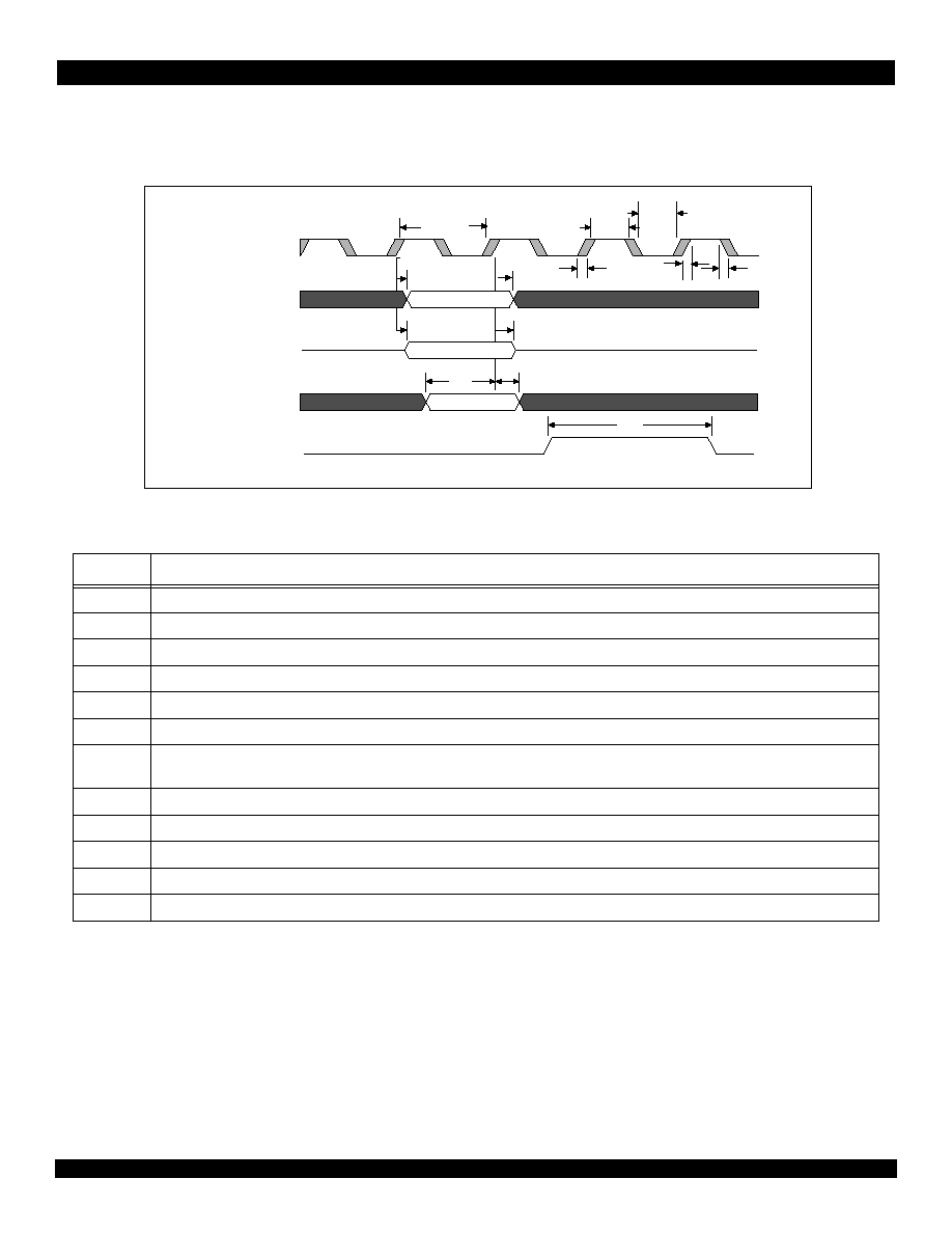
Clock Parameters
(Ta = 0
∞C to +70∞C Commercial, Ta = -40∞C to +85∞C Industrial, Vcc I/O = +3.3V±5%,V
cc
Core and V
cc
P = +2.5V
±5%)
Figure 4 Clock Parameters Waveform
Parameter
Symbol
Reference
Edge
133MHz
150MHz
180MHz
Units
Timing
Diagram
Reference
Min
Max
Min
Max
Min
Max
Internal CPU pipeline clock
1
Frequency
none
100
133
100
150
100
180
MHz
Figure 4
CLKP
2,3,4
Frequency
none
25
67
25
75
25
90
MHz
Tperiod1
15
40
13.3
40
11.1
40
ns
Thigh1
6
--
5.4
--
5.4
--
ns
Tlow1
6
--
5.4
--
5.4
--
ns
Trise1
--
3
--
2.5
--
2.5
ns
Tfall1
--
3
--
2.5
--
2.5
ns
Tjitter
--
±250
--
±200
--
±200
ps
1
The CPU pipeline clock speed is selected during cold reset by the boot configuration vector (see Table 2).
2
Ethernet clock (MIIRXCLKP and MIITXCLKP) frequency must be equal to or less than 1/2 CLKP frequency.
3
USB clock (USBCLKP) frequency must be less than CLKP frequency.
4
ATM Utopia clock (RXCLKP and TXCLKP) frequency must be equal to or less than 1/2 CLKP frequency.
Table 3 Clock Parameters
Tlow1
Thigh1
Tperiod1
CLKP
Trise1
Tfall1
Tjitter
Tjitter
16 of 47
May 25, 2004
IDT 79RC32355
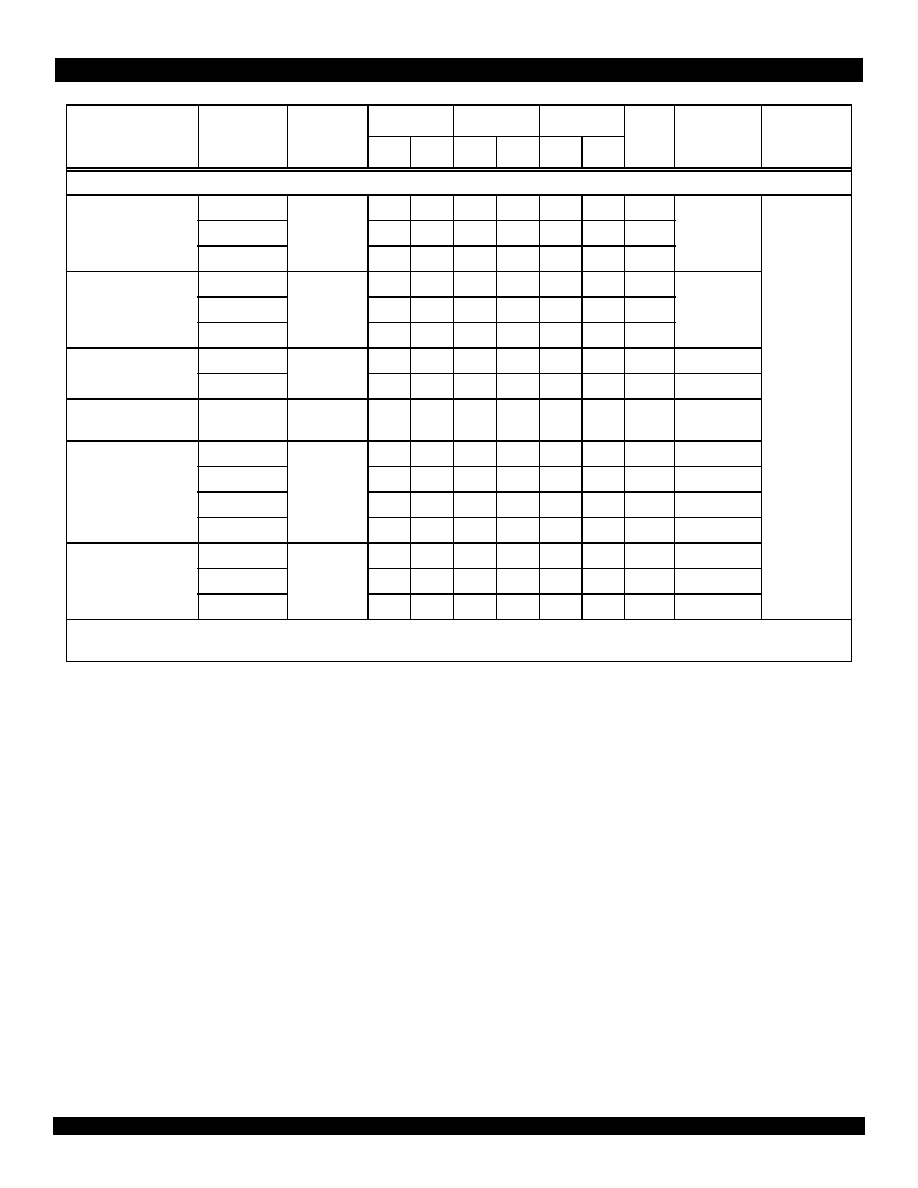
AC Timing Definitions
Below are examples of the AC timing characteristics used throughout this document.
Figure 5 AC Timing Definitions Waveform
Symbol
Definition
Tperiod
Clock period.
Tlow
Clock low. Amount of time the clock is low in one clock period.
Thigh
Clock high. Amount of time the clock is high in one clock period.
Trise
Rise time. Low to high transition time.
Tfall
Fall time. High to low transition time.
Tjitter
Jitter. Amount of time the reference clock (or signal) edge can vary on either the rising or falling edges.
Tdo
Data out. Amount of time after the reference clock edge that the output will become valid. The minimum time represents the data output hold.
The maximum time represents the earliest time the designer can use the data.
Tzd
Z state to data valid. Amount of time after the reference clock edge that the tri-stated output takes to become valid.
Tdz
Data valid to Z state. Amount of time after the reference clock edge that the valid output takes to become tri-stated.
Tsu
Input set-up. Amount of time before the reference clock edge that the input must be valid.
Thld
Input hold. Amount of time after the reference clock edge that the input must remain valid.
Tpw
Pulse width. Amount of time the input or output is active.
Table 4 AC Timing Definitions
Tdz
Tzd
Tdo
Tpw
Tpw
Thld
Tsu
Tlow
Thigh
Thigh
Tperiod
clock
Output signal 1
Output signal 2
Input Signal 1
Signal
Tjitter
Trise
Tfall
Tdo

17 of 47
May 25, 2004
IDT 79RC32355
AC Timing Characteristics
(Ta = 0
∞C to +70∞C Commercial, Ta = -40∞C to +85∞C Industrial, Vcc I/O = +3.3V±5%,V
cc
Core = +2.5V
±5%, V
cc
P = +2.5V
±5%)
Signal
Symbol
Reference
Edge
133MHz
150MHz
180MHz
Unit Conditions
Timing
Diagram
Reference
Min
Max
Min
Max
Min
Max
Reset and System
COLDRSTN
Tpw1
none
110
--
110
--
110
--
ms
Figure 6
Figure 7
Trise1
none
--
5.0
--
5.0
--
5.0
ns
RSTN
1
Tdo2
CLKP rising
4.0
10.7
4.0
10.7
4.0
10.7
ns
MDATA[15:0]
Boot Configuration
Vector
Thld3
COLDRSTN
rising
3
--
3
--
3
--
ns
INSTP
Tdo
CLKP rising
5.0
8.0
5.0
8.0
5.0
8.0
ns
CPUP
Tdo
CLKP rising
3.5
7.0
3.5
7.0
3.5
7.0
ns
DMAP
Tdo
CLKP rising
3.5
6.6
3.5
6.6
3.5
6.6
ns
DMAREQN
2
Tpw
none
(CLKP+7)
--
(CLKP+7)
--
(CLKP+7)
--
ns
DMADONEN
2
Tpw
none
(CLKP+7)
--
(CLKP+7)
--
(CLKP+7)
--
ns
DMAFIN
Tdo
CLKP rising
3.5
5.9
3.5
5.9
3.5
5.9
ns
BRN
Tsu
CLKP rising
1.6
--
1.6
--
1.6
--
ns
Thld
0
--
0
--
0
--
ns
BGN
Tdo
CLKP rising
3.3
5.8
3.3
5.8
3.3
5.8
ns
1
RSTN is a bidirectional signal. It is treated as an asynchronous input.
2
DMAREQN and DMADONEN minimum pulse width equals the CLKP period plus 7ns.
Table 5 Reset and System AC Timing Characteristics

18 of 47
May 25, 2004
IDT 79RC32355
Figure 6 Cold Reset AC Timing Waveform
Figure 7 Warm Reset AC Timing Waveform
BOOT VECT
SYSCLKP
COLDRSTN
RSTN
MDATA[31:0]
BDIRN
BOEN[0]
>= 100 ms
>=10ms
>= 4096 CLKP clock cycles
OR
>= 64 CLKP clock cycles
*
>= 4096 CLKP clock cycles
OR
>= 64 CLKP clock cycles
*
*
Selection of 4096 or 64 cycles is selected by the boot configuration vector (fast reset).
Tpw1
Tdo2
CLKP
1
FFFF_FFFF
Thld3
1.
COLDRSTN asserted by external logic.
2.
The RC32355 asserts RSTN, asserts BOEN[0] low, drives BDIRN low, and tri-states the data bus in response.
3.
External logic begins driving valid boot configuration vector on the data bus, and the RC32355 starts sampling it.
4.
External logic negates COLDRSTN and tri-states the boot configuration vector on MDATA[15:0]. The boot configuration vector must not be tri-stated before COLDRSTN is deas-
serted. The RC32355 stops sampling the boot configuration vector.
5.
The RC32355 starts driving the data bus, MDATA[31:0], deasserts BOEN[0] high, and drives BDIRN high.
6.
SYSCLKP may be held constant after this point if Hold SYSCLKP Constant is selected in the boot configuration vector.
7.
RSTN negated by RC32355.
8.
CPU begins executing by taking MIPS reset exception, and the RC32355 starts sampling RSTN as a warm reset input.
2
3
4
5
6
7
8
Trise1
Active
Deasserted
Active
CLKP
COLDRSTN
RSTN
MDATA[31:0]
Mem Control Signals
>= 4096 CLKP clock cycles
OR
>= 64 CLKP clock cycles
*
>= 4096 CLKP clock cycles
OR
>= 64 CLKP clock cycles
*
(RSTN ignored during this period
to allow pull-up to drive signal high)
*
Selection of 4096 or 64 cycles is selected by the boot configuration vector (fast reset).
1.
Warm reset condition caused by either RSTN asserted, write to reset register, or bus transaction timer time-out. The RC32355 asserts RSTN output low in response.
2.
The RC32355 tri-states the data bus, MDATA[31:0], and deasserts all memory control signals, such as RASN, CASN, RWN, OEN, etc.
3.
The RC32355 deasserts RSTN.
4.
The RC32355 starts driving the data bus, MDATA[31:0], again, but does not sample the RSTN input.
5.
CPU begins executing by taking a MIPS soft reset exception and also starts sampling the RSTN input again.
FFFF_FFFF
1
2
3
4
5

19 of 47
May 25, 2004
IDT 79RC32355
Signal
Symbol
Reference
Edge
133MHz 150MHz 180MHz
Unit
Conditions
Timing
Diagram
Reference
Min
Max
Min
Max
Min
Max
Memory and Peripheral Bus - SDRAM Access
MDATA[31:0]
Tsu1
SDCLKINP
rising
2.5
--
2.5
--
2.5
--
ns
Figure 8
Figure 9
Figure 10
Thld1
1.5
--
1.5
--
1.5
--
ns
Tdo1
SYSCLKP
rising
1.2
5.8
1.2
5.8
1.2
5.8
ns
Tdz1
--
5.0
--
5.0
--
5.0
ns
Tzd1
1.0
--
1.0
--
1.0
--
ns
MADDR[20:2],
BWEN[3:0]
Tdo2
SYSCLKP
rising
1.2
5.3
1.2
5.3
1.2
5.3
ns
CASN, RASN,
SDCSN[1:0], SDWEN
Tdo3
SYSCLKP
rising
1.2
5.3
1.2
5.3
1.2
5.3
ns
CKENP
Tdo4
SYSCLKP
rising
1.2
5.3
1.2
5.3
1.2
5.3
ns
BDIRN
Tdo5
SYSCLKP
rising
1.2
5.3
1.2
5.3
1.2
5.3
ns
BOEN[1:0]
Tdo6
SYSCLKP
rising
1.2
5.3
1.2
5.3
1.2
5.3
ns
SYSCLKP rising
Tdo7
CLKP rising
0.5
5.0
0.5
5.0
0.5
5.0
ns
SDCLKINP
Tperiod8
none
15
50
13.3
50
13.3
50
ns
Thigh8,Tlow8
6.0
--
5.4
--
5.4
--
ns
Trise8,Tfall8
--
3.0
--
2.5
--
2.5
ns
Tdelay8
SYSCLKP
rising
0
4.8
0
4.8
0
4.8
ns
Table 6 Memory and Peripheral Bus AC Timing Characteristics (Part 1 of 2)

20 of 47
May 25, 2004
IDT 79RC32355
Note: The RC32355 provides bus turnaround cycles to prevent bus contention when going from a read to write, write to read, and during
external bus ownership. For example, there are no cycles where an external device and the RC32355 are both driving. See the chapters
"Device Controller," "Synchronous DRAM Controller," and "Bus Arbitration" in the RC32355 User Reference Manual.
Memory and Peripheral Bus - Device Access
MDATA[31:0]
Tsu1
CLKP rising
2.5
--
2.5
--
2.5
--
ns
Figure 11
Figure 12
Thld1
1.5
--
1.5
--
1.5
--
ns
Tdo1
2.0
6.5
2.0
6.5
2.0
6.5
ns
Tdz1
--
9.0
--
9.0
--
9.0
ns
Tzd1
2.0
--
2.0
--
2.0
--
ns
WAITACKN, BRN
Tsu
CLKP rising
2.5
--
2.5
--
2.5
--
ns
Thld
1.5
--
1.5
--
1.5
--
ns
MADDR[21:0]
Tdo2
CLKP rising
2.0
6.0
2.0
6.0
2.0
6.0
ns
Tdz2
--
9.0
--
9.0
--
9.0
ns
Tzd2
2.0
--
2.0
--
2.0
--
ns
MADDR[25:22]
Tdo3
CLKP rising
2.5
6.5
2.5
6.5
2.5
6.5
ns
Tdz3
--
9.0
--
9.0
--
9.0
ns
Tzd3
2.0
--
2.0
--
2.0
--
ns
BDIRN, BOEN[0]
Tdo4
CLKP rising
2.0
6.0
2.0
6.0
2.0
6.0
ns
Tdz4
--
9.0
--
9.0
--
9.0
ns
Tzd4
2.0
--
2.0
--
2.0
--
ns
BGN, BWEN[3:0], OEN,
RWN
Tdo5
CLKP rising
2.0
6.0
2.0
6.0
2.0
6.0
ns
Tdz5
--
9.0
--
9.0
--
9.0
ns
Tzd5
2.0
--
2.0
--
2.0
--
ns
CSN[3:0]
Tdo6
CLKP rising
1.7
5.0
1.7
5.0
1.7
5.0
ns
Tdz6
--
9.0
--
9.0
--
9.0
ns
Tzd6
2.0
--
2.0
--
2.0
--
ns
CSN[5:4]
Tdo7
CLKP rising
2.5
6.0
2.5
6.0
2.5
6.0
ns
Tdz7
--
9.0
--
9.0
--
9.0
ns
Tzd7
2.0
--
2.0
--
2.0
--
ns
Signal
Symbol
Reference
Edge
133MHz 150MHz 180MHz
Unit
Conditions
Timing
Diagram
Reference
Min
Max
Min
Max
Min
Max
Table 6 Memory and Peripheral Bus AC Timing Characteristics (Part 2 of 2)

21 of 47
May 25, 2004
IDT 79RC32355
Figure 8 Memory and Peripheral Bus AC Timing Waveform - SDRAM Read Access
Figure 9 SYSCLKP - SDCLKINP Relationship
Addr
1111
BE's
1111
NOP
READ
NOP
11
Chip-Sel
11
11
Buffer Enables
11
Data
Tzd1
Tdz1
Tdo6
Tdo6
Tdo5
Tdo5
Tdo3
Tdo3
Tdo2
Tdo2
Thld1
Tsu1
CLKP
SYSCLKP
MADDR[21:0]
BWEN[3:0]
CMD[2:0]*
SDCSN[1:0]
BDIRN
BOEN[1:0]
MDATA[31:0]
SDCLKINP
SDRAM CAS Latency
Tdo7
Tdelay8
* NOTE: CMD[2:0] = {RASN, CASN, SDWEN}
RC32355
samples
read data
RC32355
SDRAM
SRAM,
EPROM,
etc.
external
SYSCLKP
SDCLKINP
CLKLP
Memory Bus
Tdelay8
RSTN
COLDRSTN
Vcc
pull-up
buffer

22 of 47
May 25, 2004
IDT 79RC32355
Figure 10 Memory and Peripheral Bus AC Timing Waveform - SDRAM Write Access
Addr
1111
BE's
1111
NOP
WRITE
NOP
11
Chip-Sel
11
11
Buff Enable
11
Data
Tdo1
Tdo6
Tdo5
Tdo3
Tdo3
Tdo2
Tdo2
CLKP
SYSCLKP
MADDR[21:0]
BWEN[3:0]
CMD[2:0]*
SDCSN[1:0]
BDIRN
BOEN[1:0]
MDATA[31:0]
Tdo7
* NOTE: CMD[2:0] = {RASN, CASN, SDWEN}
SDRAM
samples
write data

23 of 47
May 25, 2004
IDT 79RC32355
Figure 11 Memory and Peripheral Bus AC Timing Waveform - Device Read Access
Addr[21:0]
Addr[25:22]
1111
Data
Tdo4
Tdo4
Tdo4
Tdo4
Tzd1
Tdz1
Tdo5
Tdo5
Tdo6
Tdo6
Tdo3
Tdo2
Thld1
Tsu1
CLKP
MADDR[21:0]
MADDR[25:22]
RWN
CSN[3:0]
BWEN[3:0]
OEN
MDATA[31:0]
BDIRN
BOEN[0]
WAITACKN
RC32355
samples
read data

24 of 47
May 25, 2004
IDT 79RC32355
Figure 12 Memory AC and Peripheral Bus Timing Waveform - Device Write Access
Addr[21:0]
Addr[25:22]
1111
Byte Enables
1111
Data
Tdo4
Tdo1
Tdo5
Tdo6
Tdo5
Tdo3
Tdo2
CLKP
MADDR[21:0]
MADDR[25:22]
RWN
CSNx
BWEN[3:0]
OEN
MDATA[31:0]
BDIRN
BOEN[0]
WAITACKN
25 of 47
May 25, 2004
IDT 79RC32355
Signal
Symbol
Reference
Edge
133MHz
150MHz
180MHz
Unit Conditions
Timing
Diagram
Reference
Min
Max
Min
Max
Min
Max
Ethernet
1,2
MIIRXCLKP, MIITXCLKP
Tperiod1
none
399.96 400.04 399.96 400.04 399.96 400.04
ns
10 Mbps
Figure 13
Thigh1,Tlow1
140
260
140
260
140
260
ns
Trise1,Tfall1
--
3
--
3
--
3
ns
MIIRXCLKP, MIITXCLKP
Tperiod1
none
39.996 40.004 39.996 40.004 39.996 40.004
ns
100 Mbps
Thigh1,Tlow1
14
26
14
26
14
26
ns
Trise1,Tfall1
--
2
--
2
--
2
ns
MIIRXDP[3:0],
MIIRXDVP, MIIRXERP
Tsu2
MIIRXCLKP
rising
5
--
5
--
5
--
ns
Thld2
3
--
3
--
3
--
ns
MIITXDP[3:0], MIITXENP,
MIITXERP
Tdo3
MIITXCLKP
rising
7
13
7
13
7
13
ns
MIIMDCP
Tperiod4
none
30
--
27
--
27
--
ns
Thigh4,Tlow4
14
--
13
--
13
--
ns
Trise4
--
11
--
11
--
11
ns
Tfall4
--
8
--
8
--
8
ns
MIIMDIOP
Tsu5
MIIMDCP
rising
6
--
6
--
6
--
ns
Thld5
0.5
--
0.5
--
0.5
--
ns
Tdo5
3
7
3
7
3
7
ns
1
Ethernet clock (MIIRXCLKP and MIITXCLKP) frequency must be equal to or less than 1/2 CLKP frequency.
2
MIICOLP and MIICRSP are asynchronous signals.
Table 7 Ethernet AC Timing Characteristics

26 of 47
May 25, 2004
IDT 79RC32355
Figure 13 Ethernet AC Timing Waveform
Tdo5
Tdo5
Tdo3
Tdo3
Thld5
Tsu5
Tlow4
Tlow4
Thigh4
Tperiod4
Tlow1
Tlow1
Thigh1
Tperiod1
Thld2
Tsu2
Tlow1
Tlow1
Thigh1
Tperiod1
MIIRXCLKP
MIIRXDVP, MIIRXDP[3:0], MIIRXERP
MIITXCLKP
MIITXENP, MIITXDP[3:0], MMTXERP
MIIMDCP
MIIMDIOP (output)
MIIMDIOP (input)

27 of 47
May 25, 2004
IDT 79RC32355
Signal
Symbol
Reference
Edge
133MHz 150MHz 180MHz
Unit
Conditions
Timing
Diagram
Reference
Min
Max
Min
Max
Min
Max
ATM Interface, Utopia Mode
1, 2
1.
ATM Utopia clock (RXCLKP and TXCLKP) frequency must be equal to or less than 1/2 CLKP frequency.
2.
All Utopia Mode pins are multiplexed on the ATM interface pins as described in Table 9.
RXCLKP, TXCLKP
1
Tperiod1
none
--
40
--
40
--
40
ns
25 MHz Utopia
Figure 14
Thigh1,Tlow1
16
--
16
--
16
--
ns
Trise1,Tfall1
--
4
--
4
--
4
ns
RXCLKP, TXCLKP
1
Tperiod1
none
--
30
--
30
--
30
ns
33 MHz Utopia
Thigh1,Tlow1
12
--
12
--
12
--
ns
Trise1,Tfall1
--
3
--
3
--
3
ns
RXCLKP, TXCLKP
Tperiod1
none
--
20
--
20
--
20
ns
50 MHz Utopia
Thigh,Tlow1
8
--
8
--
8
--
ns
Trise1,Tfall1
--
2
--
2
--
2
ns
TXFULLN
Tsu2
TXCLKP
rising
2
--
2
--
2
--
ns
Thld2
2
--
2
--
2
--
ns
TXDATA[7:0], TXSOC,
TXENBN, TXADDR[1:0]
Tdo3
TXCLKP
rising
4
8
4
8
4
8
ns
RXDATA[7:0], RXEMP-
TYN, RXSOC
Tsu4
RXCLKP
rising
3
--
3
--
3
--
ns
Thld4
2
--
2
--
2
--
ns
RXADDR[1:0], RXENBN
Tdo5
RXCLKP
rising
3
8
3
8
3
8
ns
Table 8 ATM AC Timing Characteristics

28 of 47
May 25, 2004
IDT 79RC32355
Figure 14 ATM AC Timing Waveform
Tdo8
Tdo7
Tdo5
Tdo3
Thld10
Tsu10
Thld9
Tsu9
Tperiod6
Tperiod6
Tperiod6
Tperiod6
Thld4
Tsu4
Tperiod1
Tperiod1
Thld2
Tsu2
Tperiod1
Tperiod1
TXCLKP
TXFULL
TXDATA,TXSOC,TXENB,TXADDR
RXCLKP
RXDATA, RXEMPTY, RXSOC
RXADDR, RXENB
O0CLKP, O1CLKP
O0DP, O0FRMP
O1DP, O1FRMP
I0CLKP, I1CLKP
I0DP
I1DP

29 of 47
May 25, 2004
IDT 79RC32355
ATM Pin Name
Utopia Level 1
Utopia Level 2
ATMINP[0]
RXDATA[0]
RXDATA[0]
ATMINP[1]
RXDATA[1]
RXDATA[1]
ATMINP[2]
RXDATA[2]
RXDATA[2]
ATMINP[3]
RXDATA[3]
RXDATA[3]
ATMINP[4]
RXDATA[4]
RXDATA[4]
ATMINP[5]
RXDATA[5]
RXDATA[5]
ATMINP[6]
RXDATA[6]
RXDATA[6]
ATMINP[7]
RXDATA[7]
RXDATA[7]
ATMINP[8]
RXCLKP
RXCLKP
ATMINP[9]
RXEMPTYN
RXEMPTYN
ATMINP[10]
RXSOC
RXSOC
ATMINP[11]
TXFULLN
TXFULLN
ATMIOP[0]
RXENBN
RXENBN
ATMIOP[1]
TXCLKP
TXCLKP
ATMOUTP[0]
TXDATA[0]
TXDATA[0]
ATMOUTP[1]
TXDATA[1]
TXDATA[1]
ATMOUTP[2]
TXDATA[2]
TXDATA[2]
ATMOUTP[3]
TXDATA[3]
TXDATA[3]
ATMOUTP[4]
TXDATA[4]
TXDATA[4]
ATMOUTP[5]
TXDATA[5]
TXDATA[5]
ATMOUTP[6]
TXDATA[6]
TXDATA[6]
ATMOUTP[7]
TXDATA[7]
TXDATA[7]
ATMOUTP[8]
TXSOC
TXSOC
ATMOUTP[9]
TXENBN
TXENBN
GPIOP[22]
TXADDR[0]
GPIOP[23]
TXADDR[1]
GPIOP[24]
RXADDR[0]
GPIOP[25]
RXADDR[1]
Table 9 ATM I/O Pin Multiplexing

30 of 47
May 25, 2004
IDT 79RC32355
Figure 15 TDM AC Timing Waveform, Master Mode
Signal
Symbol Reference
Edge
133MHz 150MHz 180MHz
Unit Conditions
Timing
Diagram
Reference
Min
Max
Min
Max
Min
Max
TDM
TDMCLKP
1
Tperiod1
none
--
125
--
62.5
--
62.5
ns
Figure 15
Figure 16
Thigh1
62.5
--
31.2
--
31.2
--
ns
Tlow1
62.5
--
31.2
--
31.2
--
ns
Trise1
--
3
--
3
--
3
ns
Tfall1
--
3
--
3
--
3
ns
TDMFP
Tsu2
TDMCLKP
rising or falling
4
--
4
--
4
--
ns
Thld2
1
--
1
--
1
--
ns
Tdo2
2
9
2
9
2
9
ns
TDMDIP
Tsu3
TDMCLKP
rising or falling
4
--
4
--
4
--
ns
Thld3
1
--
1
--
1
--
ns
TDMDOP
Tdo4
TDMCLKP
rising or falling
2
9
2
9
2
9
ns
Tdz4
--
12
--
12
--
12
ns
Tzd4
3
--
3
--
3
--
ns
TDMTEN
Tdo5
TDMCLKP
rising or falling
2
9
2
9
2
9
ns
1
The rising or falling edge of TDMCLKP is used as the reference clock edge for the timing depending on the TDM bus mode and protocol selection.
Table 10 TDM AC Timing Characteristics
Tdo5
Tdo4
Tdo4
Tdo2
Tdo2
Thld3
Tsu3
TDMCLKP
TDMFP
TDMDOP
TDMDIP
TDMTEN
Tperiod1
Tlow1
Thigh1
Trise1
Tfall1

31 of 47
May 25, 2004
IDT 79RC32355
Figure 16 TDM AC Timing Waveform, Slave Mode
Tdo5
Tdo5
Tdo4
Tdo4
Thld3
Tsu3
Thld2
Tsu2
TDMCLKP
TDMFP
TDMDOP
TDMDIP
TDMTEN

32 of 47
May 25, 2004
IDT 79RC32355
Signal
Symbol
Reference
Edge
133MHz
150MHz
180MHz
Unit
Conditions
Timing
Diagram
Reference
Min
Max
Min
Max
Min
Max
USB
USBCLKP
1
Tperiod1
none
19.79 21.87 19.79 21.87 19.79 21.87
ns
Figure 17
Thigh1,Tlow1
8.3
--
8.3
--
8.3
--
ns
Trise1,Tfall1
--
3
--
3
--
3
ns
Tjitter1
--
0.8
--
0.8
--
0.8
ns
1/4th of the mini-
mum Source data
jitter
USBDN, USBDP
Trise2
4
20
4
20
4
20
ns
Universal Serial Bus
Specification
(USBS) Revision
1.1: Figures 7.6 and
7.7.
Tfall2
4
20
4
20
4
20
ns
USBS Revision 1.1:
Figures 7.6 and 7.7.
USBDN and USBDP
Rise and Fall Time
Matching
90
111.11
90
111.11
90
111.11
%
USBS Revision 1.1:
Note 10, Section
7.1.2.
Data valid period
Tstate
60
--
60
--
60
--
ns
Skew between USBDN
and USBDP
--
0.4
--
0.4
--
0.4
ns
USBS Revision 1.1:
Section 7.1.3
Source data jitter
--
3.5
--
3.5
--
3.5
ns
USBS Revision 1.1:
Table 7-6
Receive data jitter
--
12
--
12
--
12
ns
Source EOP length
Tseop
160
175
160
175
160
175
ns
Receive EOP length
Treop
82
--
82
--
82
--
ns
EOP jitter
-2
5
-2
5
-2
5
ns
Full-speed Data Rate
Tfdrate
11.97 12.03 11.97 12.03 11.97 12.03
MHz
Average bit rate,
USBS Section
7.1.11.
Frame Interval
0.9995 1.0005 0.9995 1.0005 0.9995 1.0005
ms
USBS Section
7.1.12.
Consecutive Frame
Interval Jitter
--
42
--
42
--
42
ns
Without frame
adjustment.
--
126
--
126
--
126
ns
With frame adjust-
ment.
1
USB clock (USBCLKP) frequency must be less than CLKP frequency.
Table 11 USB AC Timing Characteristics

33 of 47
May 25, 2004
IDT 79RC32355
Figure 17 USB AC Timing Waveform
Signal
Symbol
Reference
Edge
133MHz 150MHz 180MHz
Unit Conditions
Timing
Diagram
Reference
Min
Max
Min
Max
Min
Max
UART
U0SINP, U0RIN, U0DCDN,
U0DSRN, U0CTSN, U1SINP,
U1DSRN, U1CTSN
Tsu
1
CLKP rising
5
--
5
--
5
--
ns
Thld
1
3
--
3
--
3
--
ns
U0SOUTP, U0DTRN, U0RTSN,
U1SOUTP, U1DTRN, U1RTSN
Tdo
1
CLKP rising
1
12
1
12
1
12
ns
1
These are asynchronous signals and the values are provided for ATE (test) only.
Table 12 UART AC Timing Characteristics
Tperiod1
Thigh1
Trise1
Tlow1
Tfall1
Tseop
Treop
90%
10%
90%
10%
Tstate
USBCLKP
Tjitter1
Trise2
Tfall2
Tfdrate
USBDN
USBDP
USBDN
USBDP

34 of 47
May 25, 2004
IDT 79RC32355
Signal
Symbol Reference
Edge
133MHz 150MHz 180MHz
Unit Conditions
Timing
Diagram
Reference
Min
Max
Min
Max
Min
Max
I
2
C
1
1.
For more information see the I
2
C-Bus specification by Philips Semiconductor
SCLP
Frequency
none
0
100
0
100
0
100
kHz
100 KHz
Figure 18
Thigh1
4.0
--
4.0
--
4.0
--
µs
Tlow1
4.7
--
4.7
--
4.7
--
µs
Trise1
--
1000
--
1000
--
1000
ns
Tfall1
--
300
--
300
--
300
ns
SDAP
Tsu2
SCLP rising
250
--
250
--
250
--
ns
Thld2
0
3.45
0
3.45
0
3.45
µs
Trise2
--
1000
--
1000
--
1000
ns
Tfall2
--
300
--
300
--
300
ns
Start or repeated start condition
Tsu3
SDAP falling
4.7
--
4.7
--
4.7
--
µs
Thld3
4.0
--
4.0
--
4.0
--
µs
Stop condition
Tsu4
SDAP rising
4.0
--
4.0
--
4.0
--
µs
Bus free time between a stop and
start condition
Tdelay5
4.7
--
4.7
--
4.7
--
µs
SCLP
Frequency
none
0
400
0
400
0
400
kHz
400 KHz
Thigh1
0.6
--
0.6
--
0.6
--
µs
Tlow1
1.3
--
1.3
--
1.3
--
µs
Trise1
--
300
--
300
--
300
ns
Tfall1
--
300
--
300
--
300
ns
SDAP
Tsu2
SCLP rising
100
--
100
--
100
--
ns
Thld2
0
0.9
0
0.9
0
0.9
µs
Trise2
--
300
--
300
--
300
ns
Tfall2
--
300
--
300
--
300
ns
Start or repeated start condition
Tsu3
SDAP falling
0.6
--
0.6
--
0.6
--
µs
Thld3
0.6
--
0.6
--
0.6
--
µs
Stop condition
Tsu4
SDAP rising
0.6
--
0.6
--
0.6
--
µs
Bus free time between a stop and
start condition
Tdelay5
1.3
--
1.3
--
1.3
--
µs
Table 13 I
2
C AC Timing Characteristics
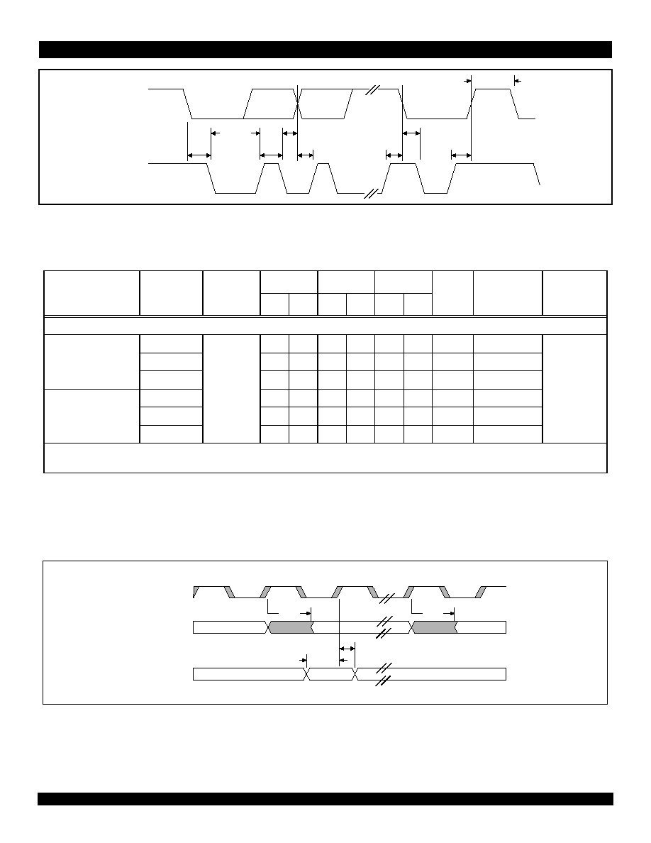
35 of 47
May 25, 2004
IDT 79RC32355
Figure 18 I
2
C AC Timing Waveform
Table 14 GPIOP AC Timing Characteristics
Figure 19 GPIOP AC Timing Waveform
Signal
Symbol
Reference
Edge
133MHz
150MHz
180MHz
Unit
Conditions
Timing
Diagram
Reference
Min
Max
Min
Max
Min
Max
GPIOP
GPIOP[31:0]
1
Tsu1
CLKP rising
4
--
4
--
4
--
ns
Figure 19
Thld1
1.4
--
1.4
--
1.4
--
ns
Tdo1
2
8
2
8
2
8
ns
GPIOP[35:32]
2
Tsu1
3
--
3
--
3
--
ns
Thld1
1
--
1
--
1
--
ns
Tdo1
3
8
3
8
3
8
ns
1
GPIOP[31:0] are controlled through the GPIO interface. GPIO[31:0] are asynchronous signals, the values are provided for ATE (test) only.
2
GPIOP[35:32] are controlled through the TDM interface.
Tsu4
Thld3
Tsu3
Tsu2
Thld2
Thigh1
Tlow1
Thld3
Tlow1
Tdelay5
Tdelay5
SDAP
SCLP
GPIOP (input)
GPIOP (output)
CLKP
Tsu1
Thld1
Tdo1
Tdo1

36 of 47
May 25, 2004
IDT 79RC32355
Table 15 JTAG AC Timing Characteristics
Figure 20 JTAG AC Timing Waveform
Signal
Symbol
Reference
Edge
133MHz
150MHz
180MHz
Unit Conditions
Timing
Diagram
Reference
Min
Max
Min
Max
Min
Max
EJTAG and JTAG
JTAG_TCK
Tperiod1
none
100
--
100
--
100
--
ns
Figure 20
Thigh1, Tlow1
40
--
40
--
40
--
ns
Trise1, Tfall1
--
5
--
5
--
5
ns
EJTAG_DCLK
1
1.
EJTAG_DCLK is equal to the internal CPU pipeline clock.
Tperiod2
none
7.5
10.0
6.7
10.0
5.6
10.0
ns
Thigh2, Tlow2
2.5
--
2.5
--
2.5
--
ns
Trise2, Tfall2
--
3.5
--
3.5
--
3.5
ns
JTAG_TMS, JTAG_TDI,
JTAG_TRST_N
Tsu3
JTAG_TCK rising
3.0
--
3.0
--
3.0
--
ns
Thld3
1.0
--
1.0
--
1.0
--
ns
JTAG_TDO
Tdo4
JTAG_TCK falling
2.0
12.0
2
12.0
2
12.0
ns
Tdo5
EJTAG_DCLK rising -0.7
2
2.
A negative delay denotes the amount of time before the reference clock edge.
1.0
-0.7
2
1.0
-0.7
2
1.0
ns
JTAG_TRST_N
Tpw6
none
100
--
100
--
100
--
ns
Tsu6
JTAG_TCK rising
2
--
2
--
2
--
ns
EJTAG_PCST[2:0]
Tdo7
EJTAG_DCLK rising -0.3
2
3.3
-0.3
2
3.3
-0.3
2
3.3
ns
Tperiod1
Tfall1
Tlow1
Thigh1
Trise2
Tfall2
Thigh2
Tlow2
Tsu3
Thld3
Tdo4
Tperiod2
Trise1
Tdo5
Tdo7
Tsu6
Tpw6
JTAG_TCK
EJTAG_DCLK
JTAG_TMS,
JTAG_TDI
JTAG_TDO
EJTAG_PCST
JTAG_TRST_N
TPC
TDO
TDO
PCST
EJTAG TPC, TCST capture
EJTAG_TRST_N
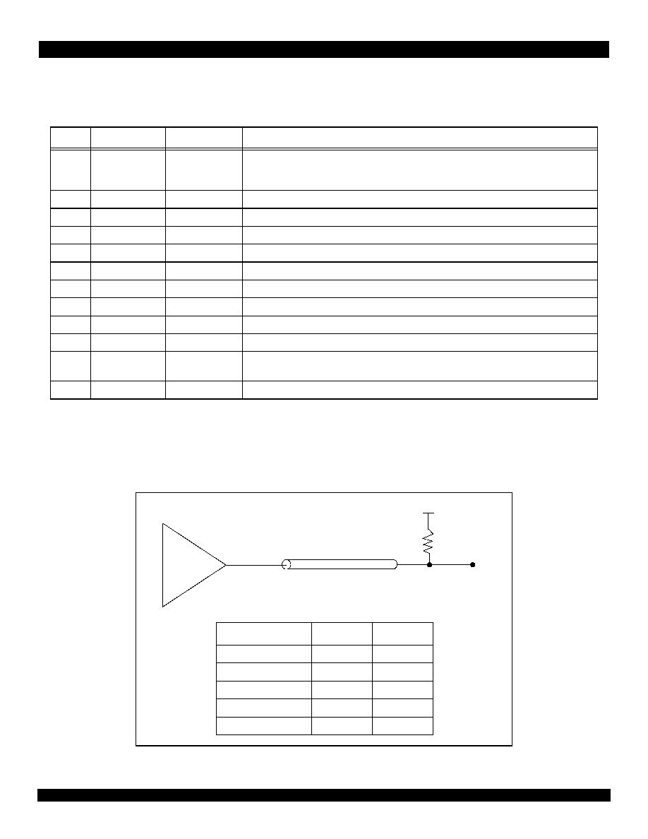
37 of 47
May 25, 2004
IDT 79RC32355
Table 16 shows the pin numbering for the Standard EJTAG connector. All the even numbered pins are connected to ground. Multiplexing of pin
functions should be considered when connecting
EJTAG_TRST_N and EJTAG_PCST.
For details on using the JTAG connector, see the JTAG chapters in the RC32355 user reference manual.
AC Test Conditions
Figure 21 Output Loading for AC Timing
PIN
SIGNAL
RC32355 I/O
TERMINATION
1
1.
The value of the series resistor may depend on the actual printed circuit board layout situation.
1
EJTAG_TRST_N
Input
10 k
pull-down resistor. A pull-down resistor will hold the EJTAG controller in reset when not in use
if the EJTAG_TRST_N function is selected with the boot configuration vector. Refer to the User Man-
ual.
3 JTAG_TDI
Input
10
k
pull-up resistor
5
JTAG_TDO
Output
33
series resistor
7 JTAG_TMS
Input
10
k
pull-up resistor
9
JTAG_TCK
Input
10 k
pull-up resistor
2
2.
JTAG_TCK pull-up resistor is not required according to the JTAG (IEEE1149) standard. It is indicated here to prevent a floating CMOS input when the EJTAG connector is
unconnected.
11
System Reset
Input
10 k
pull-up resistor is used if it is combined with the system cold reset control, COLDRSTN.
13
EJTAG_PCST[0]
Output
33
series resistor
15
EJTAG_PCST[1]
Output
33
series resistor
17
EJTAG_PCST[2]
Output
33
series resistor
19
EJTAG_DCLK
Output
33
series resistor
21
Debug Boot
Input
This can be connected to the boot configuration vector to control debug boot mode if desired. Refer
to Table 2 on page 12 and the RC32355 user reference manual.
23
V
CC
I/O
Output
Used to sense the circuit board power. Must be connected to the VCC I/O supply of the circuit board.
Table 16 Pin Numbering of the JTAG and EJTAG Target Connector
1.5V
Parameter
Value
Units
Input pulse levels
0 to 3.0
V
Input rise/fall
3.5
ns
Input reference level
1.5
V
Output reference levels
1.5
V
AC test load
25
pF
RC32355
Output
.
50
50
Test
Point
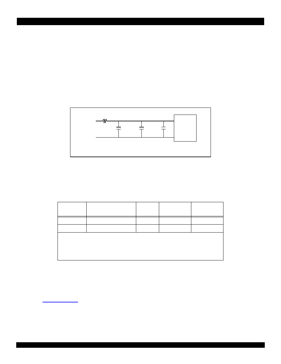
38 of 47
May 25, 2004
IDT 79RC32355
Phase-Locked Loop (PLL)
The processor aligns the pipeline clock, PClock, to the master input clock (CLKP) by using an internal phase-locked loop (PLL) circuit that gener-
ates aligned clocks. Inherently, PLL circuits are only capable of generating aligned clocks for master input clock (CLKP) frequencies within a limited
range.
PLL Analog Filter
The storage capacitor required for the Phase-Locked Loop circuit is contained in the RC32355. However, it is recommended that the system
designer provide a filter network of passive components for the PLL power supply.
V
CC
P (PLL circuit power) and V
SS
P (PLL circuit ground) should be isolated from V
CC
Core (core power) and V
SS
(common ground) with a filter
circuit such as the one shown in Figure 22.
Because the optimum values for the filter components depend upon the application and the system noise environment, these values should be
considered as starting points for further experimentation within your specific application.
Figure 22 PLL Filter Circuit for Noisy Environments
Recommended Operating Temperature and Supply Voltage
Capacitive Load Deration
Refer to the
RC32355 IBIS Model
which can be found at the IDT web site (www.idt.com).
Grade
Temperature
Vss
1
VssP
5
V
cc
I/O
2
V
cc
Core
3
V
cc
P
4
Commercial
0
∞C to +70∞C Ambient
0V
3.3V±5%
2.5V±5%
Industrial
-40
∞C+ 85∞C Ambient
0V
3.3V±5%
2.5V±5%
1
Vss supplies a common ground.
2
VccI/O is the I/O power.
3
VccCore is the internal logic power.
4
VccP is the phase lock loop power.
5
VssP is the phase lock loop ground.
Table 17 Temperature and Voltage
10
µ
F
0.1
µ
F
100 pF
Vcc
Vss
VccP
VssP
10 ohm
1
1.
This resistor may be required in noisy circuit environments.
RC32355

39 of 47
May 25, 2004
IDT 79RC32355
Power-on RampUp
The 2.5V core supply (and 2.5V V
cc
PLL supply) can be fully powered without the 3.3V I/O supply. However, the 3.3V I/O supply cannot exceed the
2.5V core supply by more than 1 volt during power up. A sustained large power difference could potentially damage the part. Inputs should not be
driven until the part is fully powered. Specifically, the input high voltages should not be applied until the 3.3V I/O supply is powered.
There is no special requirement for how fast V
cc
I/O ramps up to 3.3V. However, all timing references are based on a stable V
cc
I/O.
DC Electrical Characteristics
(T
ambient
= 0
∞C to +70∞C
Commercial
, T
ambient
= -40
∞C to +85∞C
Industrial
, Vcc I/O = +3.3V
±5%, V
cc
Core and V
cc
P = +2.5V
±
5%
)
Para-
meter
Min
Max
Unit
Pin Numbers
Conditions
LOW Drive
Output with
Schmitt Trigger
Input (STI)
I
OL
7.3
--
mA
1-4,6-8,10-16,18,20-25,27-29,32,33,35-37,
39-42,44,46-48,50,52,53,56,58-60,62-69,
71-77,82-85,87-94,96-99,101-105,167,
205-208
V
OL
= 0.4V
I
OH
-8.0
--
mA
V
OH
= (V
cc
I/O - 0.4)
V
IL
--
0.8
V
--
V
IH
2.0
(V
cc
I/O
+ 0.5)
V
--
V
OH
V
cc
- 0.4
--
V
--
HIGH Drive
Output with
Standard Input
I
OL
9.4
--
mA
49,51,54,55,106-108,110,112-117,119,
121,123-128,130,132-137,139,141,143,
150,152,154-159,161,163-166,168-170,
172,174-179,181,185-190,192,194-200,
202,204
V
OL
= 0.4V
I
OH
-15
--
mA
V
OH
= (V
cc
I/O - 0.4)
V
IL
--
0.8
V
--
V
IH
2.0
(V
cc
I/O
+ 0.5)
V
--
V
OH
V
cc
- 0.4
--
V
--
Clock Drive
Output
I
OL
39
--
mA
183
V
OL
= 0.4V
I
OH
-24
--
mA
V
OH
= (V
cc
I/O - 0.4)
Capacitance
C
IN
--
10
pF
All pins
--
Leakage
I/O
LEAK
--
20
µ
A
All pins
--
Table 18 DC Electrical Characteristics

40 of 47
May 25, 2004
IDT 79RC32355
USB Electrical Characteristics
Power Consumption
Note: This table is based on a 2:1 CPU pipeline to system (PClock to CLKP) clock ratio.
Table 20 RC32355 Power Consumption
Parameter
Min
Max
Unit
Conditions
USB Interface
V
di
Differential Input Sensitivity
-0.2
V
I(D+)-(D-)I
V
cm
Differential Input Common Mode
Range
0.8
2.5
V
V
se
Single ended Receiver Threshold
0.8
2.0
V
C
in
Transceiver Capacitance
20
pF
I
li
Hi-Z State Data Line Leakage
-10
10
µA
0V < V
in
< 3.3V
USB Upstream/Downstream Port
V
oh
Static Output High
2.8
3.6
V
15km + 5% to Gnd
V
ol
Static Output Low
0.3
V
Z
o
USB Driver Output Impedance
28
44
Including R
ext
= 20
Table 19 USB Interface Characteristics
Parameter
133MHz
150MHz
180MHz
Unit
Conditions
Typical
Max. Typical
Max. Typical
Max.
I
CC
I/O
80
130
100
150
120
170
mA
I
CC core
Normal mode
400
450
450
500
500
550
mA
C
L
= 25pF (affects I/O)
T
a
= 25
o
C
VccP = 2.625V (for max. values)
V
cc
core = 2.625V (for max. values)
V
cc
I/O
= 3.46V (for max. values)
VccP = 2.5V (for typical values)
V
cc
core = 2.5V (for typical values)
V
cc
I/O
= 3.3V (for typical values)
Standby mode
1
1.
RISCore 32300 CPU core enters Standby mode by executing WAIT instructions; however, other logic continues to function. Standby mode reduces power consumption by 0.6
mA per MHz of the CPU pipeline clock, PClock.
320
370
360
410
400
450
mA
Power
Dissipation
Normal mode
1.26
1.63
1.46
1.86
1.73
2.03
W
Standby mode
1
1.06
1.42
1.22
1.59
1.47
1.77
W

41 of 47
May 25, 2004
IDT 79RC32355
Power Curve
The following graph contains a power curve that shows power consumption at various bus frequencies.
Note: The system clock (CLKP) can be multiplied by 2, 3, or 4 to obtain the CPU pipeline clock (PClock) speed.
Figure 23 Typical Power Usage
Absolute Maximum Ratings
Symbol
Parameter
Min
1
1.
Functional and tested operating conditions are given in Table 17. Absolute maximum ratings are stress ratings only,
and functional operation at the maximums is not guaranteed. Stresses beyond those listed may affect device reliability
or cause permanent damage to the device.
Max
1
Unit
V
CC
I/O
I/O Supply Voltage
-0.3
3.465
V
V
CC
Core
Core Supply Voltage
-0.3
3.0
V
V
CC
P
PLL Supply Voltage
-0.3
3.0
V
Vimin
Input Voltage - undershoot
-0.6
--
V
Vi
I/O Input Voltage
Gnd
V
CC
I/O+0.6
V
Ta,
Industrial
Ambient Operating
Temperature
-40
85
degrees C
Tstg
Storage Temperature
-40
125
degrees C
Table 21 Absolute Maximum Ratings
Typical Power Curve
0.6
0.8
1.0
1.2
1.4
1.6
1.8
2.0
2.2
40
45
50
55
60
65
70
75
80
85
90
System Bus Speed (MHz)
P
o
wer (W @ 3.3v IO & 2.5v core)
2x

42 of 47
May 25, 2004
IDT 79RC32355
Package Pin-out -- 208-Pin PQFP
The following table lists the pin numbers and signal names for the RC32355.
Pin
Function
Alt Pin
Function
Alt Pin
Function
Alt Pin
Function
Alt
1
ATMOUTP[0]
53
JTAG_TDO
105
BGN
157
MDATA[28]
2
ATMOUTP[1]
54
GPIOP[16]
1
106
CSN[0]
158
MDATA[13]
3
ATMINP[02]
55
GPIOP[17]
1
107
CSN[1]
159
MDATA[29]
4
ATMOUTP[2]
56
GPIOP[18]
1
108
CSN[2]
160
Vcc I/O
5
Vss
57
Vss
109
Vcc I/O
161
MDATA[14]
6
ATMOUTP[3]
58
JTAG_TCK
110
CSN[3]
162
Vss
7
ATMINP[03]
59
GPIOP[19]
1
111
Vss
163
MDATA[30]
8
ATMOUTP[4]
60
GPIOP[20]
1
112
OEN
164
MDATA[15]
9
Vcc I/O
61
Vcc I/O
113
RWN
165
MDATA[31]
10
ATMOUTP[5]
62
GPIOP[21]
1
114
BDIRN
166
CLKP
11
ATMINP[04]
63
JTAG_TDI
115
BOEN[0]
167
WAITACKN
12
ATMOUTP[6]
64
GPIOP[22]
1
116
BOEN[1]
168
MADDR[00]
13
ATMOUTP[7]
65
GPIOP[23]
2
117
BWEN[0]
169
MADDR[11]
14
ATMINP[05]
66
GPIOP[24]
1
118
Vcc I/O
170
MADDR[01]
15
ATMOUTP[8]
67
JTAG_TMS
119
BWEN[1]
171
Vcc I/O
16
ATMOUTP[9]
68
GPIOP[25]
2
120
Vss
172
MADDR[12]
17
Vss
69
GPIOP[26]
1
121
BWEN[2]
173
Vss
18
ATMINP[06]
70
Vss
122
Vcc Core
174
MADDR[02]
19
Vcc Core
71
GPIOP[27]
1
123
BWEN[3]
175
MADDR[13]
20
GPIOP[00]
1
72
COLDRSTN
124
MDATA[00]
176
MADDR[03]
21
GPIOP[01]
1
73
GPIOP[28]
1
125
MDATA[16]
177
MADDR[14]
22
ATMINP[07]
74
GPIOP[29]
1
126
MDATA[01]
178
MADDR[04]
23
GPIOP[02]
2
75
GPIOP[30]
1
127
MDATA[17]
179
MADDR[15]
24
GPIOP[03]
1
76
GPIOP[31]
2
128
MDATA[02]
180
Vcc I/O
25
ATMINP[08]
77
USBCLKP
129
Vcc I/O
181
MADDR[05]
26
Vcc I/O
78
Vcc I/O
130
MDATA[18]
182
Vcc Core
27
GPIOP[04]
2
79
USBDN
131
Vss
183
SYSCLKP
28
GPIOP[05]
1
80
USBDP
132
MDATA[03]
184
Vss
29
ATMINP[09]
81
Vss
133
MDATA[19]
185
MADDR[16]
30
VccP
1
82
MIICRSP
134
MDATA[04]
186
MADDR[06]
31
VssP
1
83
MIICOLP
135
MDATA[20]
187
MADDR[17]
32
ATMINP[10]
84
MIITXDP[0]
136
MDATA[05]
188
MADDR[07]
33
GPIOP[06]
1
85
MIITXDP[1]
137
MDATA[21]
189
MADDR[18]
34
Vss
86
Vcc Core
138
Vcc Core
190
MADDR[08]
Table 22: 208-pin QFP Package Pin-Out (Part 1 of 2)

43 of 47
May 25, 2004
IDT 79RC32355
35
GPIOP[07]
1
87
MIITXDP[2]
139
MDATA[06]
191
Vcc I/O
36
ATMINP [11]
88
MIITXDP[3]
140
Vcc I/O
192
MADDR[19]
37
GPIOP[08]
2
89
MIITXENP
141
MDATA[22]
193
Vss
38
Vcc Core
90
MIITXCLKP
142
Vss
194
MADDR[09]
39
GPIOP[09]
2
91
MIITXERP
143
MDATA[07]
195
MADDR[20]
40
GPIOP[10]
2
92
MIIRXERP
144
MDATA[23]
196
MADDR[10]
41
GPIOP[11]
2
93
MIIRXCLKP
145
SDCLKINP
197
MADDR[21]
42
GPIOP[12]
2
94
MIIRXDVP
146
MDATA[08]
198
CASN
43
Vcc I/O
95
Vcc I/O
147
MDATA[24]
199
RASN
44
GPIOP[13]
2
96
MIIRXDP[0]
148
MDATA[09]
200
SDWEN
45
Vss
97
MIIRXDP[1]
149
MDATA[25]
201
Vcc I/O
46
GPIOP[14]
1
98
MIIRXDP[2]
150
MDATA[10]
202
SDCSN[0]
47
GPIOP[15]
1
99
MIIRXDP[3]
151
Vcc I/O
203
Vss
48
GPIOP[35]
1
100
Vss
152
MDATA[26]
204
SDCSN[1]
49
GPIOP[34]
1
101
MIIDCP
153
Vss
205
ATMINP[00]
50
GPIOP[33]
1
102
MIIDIOP
154
MDATA[11]
206
ATMIOP[0]
51
GPIOP[32]
1
103
RSTN
155
MDATA[27]
207
ATMIOP[1]
52
INSTP
104
BRN
156
MDATA[12]
208
ATMINP[01]
1
VccP and VssP are the Phase Lock Loop (PLL) power and ground. PLL power and ground should be supplied through a special filter circuit.
Pin
Function
Alt Pin
Function
Alt Pin
Function
Alt Pin
Function
Alt
Table 22: 208-pin QFP Package Pin-Out (Part 2 of 2)

44 of 47
May 25, 2004
IDT 79RC32355
Alternate Pin Functions
Table 23 Alternate Pin Functions
Pin
Primary
Alt #1
Alt #2
Pin
Primary
Alt #1
Alt #2
20
GPIOP[00]
U0SOUTP
51
GPIOP[32]
TDMDOP
21
GPIOP[01]
U0SINP
54
GPIOP[16]
CSN[4]
23
GPIOP[02]
U0RIN
JTAG_TRST_N
55
GPIOP[17]
CSN[5]
24
GPIOP[03]
U0DCRN
56
GPIOP[18]
DMAREQN
27
GPIOP[04]
U0DTRN
CPUP
59
GPIOP[19]
DMADONEN
28
GPIOP[05]
U0DSRN
60
GPIOP[20]
USBSOF
33
GPIOP[06]
U0RTSN
62
GPIOP[21]
CKENP
35
GPIOP[07]
U0CTSN
64
GPIOP[22]
TXADDR[0]
37
GPIOP[08]
U1SOUTP
DMAP[3]
65
GPIOP[23]
TXADDR[1]
DMAP[0]
39
GPIOP[09]
U1SINP
DMAP[2]
66
GPIOP[24]
RXADDR[0]
40
GPIOP[10]
U1DTRN
EJTAG_PCST[0]
68
GPIOP[25]
RXADDR[1]
DMAP[1]
41
GPIOP[11]
U1DSRN
EJTAG_PCST[1]
69
GPIOP[26]
TDMTEN
42
GPIOP[12]
U1RTSN
EJTAG_PCST[2]
71
GPIOP[27]
MADDR[22]
44
GPIOP[13]
U1CTSN
EJTAG_DCLK
73
GPIOP[28]
MADDR[23]
46
GPIOP[14]
SDAP
74
GPIOP[29]
MADDR[24]
47
GPIOP[15]
SCLP
75
GPIOP[30]
MADDR[25]
48
GPIOP[35]
TDMCLKP
76
GPIOP[31]
DMAFIN
EJTAG_TRST_N
49
GPIOP[34]
TDMFP
50
GPIOP[33]
TDMDIP
45 of 47
May 25, 2004
IDT 79RC32355
Package Drawing - 208-pin QFP

46 of 47
May 25, 2004
IDT 79RC32355
Package Drawing - page two

47 of 47
May 25, 2004
IDT 79RC32355
CORPORATE HEADQUARTERS
2975 Stender Way
Santa Clara, CA 95054
for SALES:
800-345-7015 or 408-727-6116
fax: 408-330-1748
www.idt.com
for Tech Support:
email: rischelp@idt.com
phone: 408-492-8208
Ordering Information
Valid Combinations
79RC32T355 -133DH, 150DH, 180DH
208-pin QFP package, Commercial Temperature
79RC32T355 -133DHI, 150DHI
208-pin QFP package, Industrial Temperature
79RCXX
YY
XXXX
999
A
A
Operating
Voltage
Device
Type
Speed
Package
Temp range/
Process
T
133
Blank
Commercial Temperature
(0∞C to +70∞C Ambient)
133 MHz Pipeline Clk
2.5V +/-5% Core Voltage
Integrated Core Processor
Product
Type
79RC32
32-bit Embedded
Microprocessor
208-pin QFP
DH
150
150 MHz Pipeline Clk
355
I
Industrial Temperature
(-40∞ C to +85∞ C Ambient)
180
180 MHz Pipeline Clk