 | –≠–ª–µ–∫—Ç—Ä–æ–Ω–Ω—ã–π –∫–æ–º–ø–æ–Ω–µ–Ω—Ç: 82V2058 | –°–∫–∞—á–∞—Ç—å:  PDF PDF  ZIP ZIP |

FEATURES
Fully integrated octal E1 short haul line interface which
supports 120
E1 twisted pair and 75
E1 coaxial appli-
cations
Selectable single rail or dual rail mode and AMI or HDB3
line encoder/decoder
Built-in transmit pre-equalization meets G.703
Selectable transmit/receive jitter attenuator meets ETSI
CTR12/13, ITU G.736, G.742 and G.823 specifications
SONET/SDH optimized jitter attenuator meets ITU G.783
mapping jitter specification
Digital/analog LOS detector meets ITU G.775 and ETS 300
233
OCTAL E1 SHORT HAUL
LINE INTERFACE UNIT
IDT82V2058
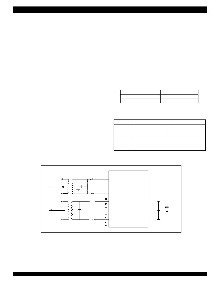
FUNCTIONAL BLOCK DIAGRAM
Jitter
Attenuator
Jitter
Attenuator
HDB3/AMI
Decoder
HDB3/AMI
Encoder
Remote
Loopback
Analog
Loopback
Slicer
Peak
Detector
CLK&Data
Recovery
(DPLL)
Line
Driver
Waveform
Shaper
LOS
Detector
Digital
Loopback
AIS
Detector
One of Eight Identical Channels
Register
File
Clock
Generator
MODE[2:0]
CS
/JAS
SCLK/ALE/
AS
RD
/R/
W
SDI/
WR
/
DS
SD0/RDY/
ACK INT
LP/D/AD[7:0]
MC/A[4:0]
OE
MCLK
TRST TCK TMS TDI TDO
JTAG TAP
RTIPn
RRINGn
TTIPn
TRINGn
VDD IO
VDDT
VDDD
VDDA
LOSn
RCLKn
RDn/RDPn
CVn/RDNn
TCLKn
BPVIn/TDNn
TDn/TDPn
G.772
Monitor
Transmit
All Ones
Control Interface
CLKE
Figure - 1. Block Diagram
The IDT logo is a registered trademark of Integrated Device Technology, Inc.
INDUSTRIAL TEMPERATURE RANGES
1
JANUARY 2003
DSC-6038/9
©
2002 Integrated Device Technology, Inc.
ITU G.772 non-intrusive monitoring for in-service testing
for any one of channel1 to channel7
Low impedance transmit drivers with tri-state
Selectable hardware and parallel/serial host interface
Local and remote loopback test functions
Hitless Protection Switching (HPS) for 1 to 1 protection
without relays
JTAG boundary scan for board test
3.3V supply with 5V tolerant I/O
Low power consumption
Operating temperature range: -40∞C to +85∞C
Available in 144-pin Thin Quad Flat Pack (TQFP_144_DA)
and 160-pin Plastic Ball Grid Array (PBGA) packages

2
INDUSTRIAL TEMPERATURE RANGES
IDT82V2058 OCTAL E1 SHORT HAUL LINE INTERFACE UNIT
Figure - 2. TQFP144 Package Pin Assignment
DESCRIPTION:
The IDT82V2058 is a single chip, 8-channel E1 short haul PCM
transceiver with a reference clock of 2.048MHz. It contains 8 transmit-
ters and 8 receivers.
Both receivers and transmitters can be programmed to work either
in single rail mode or dual rail mode. AMI or HDB3 encoder/decoder
is selectable in single rail mode. Pre-encoded transmit data in NRZ
format can be accepted when the device is configured in dual rail
mode. The receivers perform clock and data recovery by using
integrated digital phase-locked loop. As an option, the raw sliced data
(no retiming) can be output on the receive data pins. Transmit
equalization is implemented with low-impedance output drivers that
provide shaped waveforms to the transformer, guaranteeing template
conformance.
A jitter attenuator is integrated in the IDT82V2058 and can be
switched into either the transmit path or the receive path. The jitter at-
PIN CONFIGURATIONS
tenuation performance meets ETSI CTR12/13, ITU G.736, G.742, and
G.823 specifications.
The IDT82V2058 offers hardware control mode and software con-
trol mode. Software control mode works with either serial host interface
or parallel host interface. The latter works via an Intel/Motorola com-
patible 8-bit parallel interface for both multiplexed or non-
multiplexed applications. Hardware control mode uses
multiplexed pins to select different operation mode when host in-
terface is not available to the device.
The IDT82V2058 also provides loopback testing functions and
JTAG boundary scan testing functions. As the monitoring function is
integrated, IDT82V2058 can be configured as a 7-channel transceiver
with non-intrusive protected monitoring points.
The IDT82V2058 can be used for SDH/SONET multiplexers, cen-
tral office or PBX, digital access cross connects, digital radio base sta-
tions, remote wireless modules and microwave transmission systems.
BPVI3/TDN3
RCLK3
RD3/RDP3
CV3/RDN3
LOS3
RTIP3
RRING3
VDDT3
TTIP3
TRING3
GNDT3
RRING2
RTIP2
GNDT2
TRING2
TTIP2
VDDT2
RTIP1
RRING1
VDDT1
TTIP1
TRING1
GNDT1
RRING0
RTIP0
GNDT0
TRING0
TTIP0
VDDT0
MODE1
LOS0
CV0/RDN0
RD0/RDP0
RCLK0
BPVI0/TDN0
TD0/TDP0
1 2 3 4
5 6 7 8 9 10
1
1 12 13 14 15 16 17 18 19 20 21 22 23 24 25 26 27 28 29 30 31 32 33 34 35 36
72
71
70
69
68
67
66
65
64
63
62
61
60
59
58
57
56
55
54
53
52
51
50
49
48
47
46
45
44
43
42
41
40
39
38
37
108 107 106 105
104 103 102 101 100 99
98 97 96 95 94 93
92 91 90 89 88
87 86 85 84 83 82
81 80 79 78 77 76
75 74 73
109
110
111
112
113
114
115
116
117
118
119
120
121
122
123
124
125
126
127
128
129
130
131
132
133
134
135
136
137
138
139
140
141
142
143
144
TD7/TDP7
TCLK7 LOS6
CV6/RDN6
RD6/RDP6
RCLK6
BPVI6/TDN6
TD6/TDP6
TCLK6 MCLK
MODE2
A4
MC3/A3 MC2/A2 MC1/A1 MC0/A0
VDDIO GNDIO VDDD GNDD
LP0/D0/AD0
LP1/D1/AD1 LP2/D2/AD2 LP3/D3/AD3 LP4/D4/AD4 LP5/D5/AD5 LP6/D6/AD6
LP7/D7/AD7
TCLK1
TD1/TDP1
BPVI1/TDN1
RCLK1
RD1/RDP1
CV1/RDN1
LOS1 TCLK0
TD4/TDP4 TCLK4 LOS5 CV5/RDN5
RD5/RDP5 RCLK5 BPVI5/TDN5 TD5/TDP5 TCLK5 TDI
TDO TCK TMS TRST IC IC
VDDIO GNDIO VDDA GNDA MODE0/CODE
CS
/JAS
SCLK/ALE/
AS
RD
/R/
W
SDI/
WR
/
DS
SDO/RDY/
ACK
INT
TCLK2 TD2/TDP2 BPVI2/TDN2 RCLK2 RD2/RDP2 CV2/RDN2
LOS2 TCLK3 TD3/TDP3
BPVI4/TDN4
RCLK4
RD4/RDP4
CV4/RDN4
LOS4
OE
CLKE
VDDT4
TTIP4
TRING4
GNDT4
RTIP4
RRING4
GNDT5
TRING5
TTIP5
VDDT5
RRING5
RTIP5
VDDT6
TTIP6
TRING6
GNDT6
RTIP6
RRING6
GNDT7
TRING7
TTIP7
VDDT7
RRING7
RTIP7
LOS7
CV7/RDN7
RD7/RDP7
RCLK7
BPVI7/TDN7
IDT
82V2058DA

3
INDUSTRIAL TEMPERATURE RANGES
IDT82V2058 OCTAL E1 SHORT HAUL LINE INTERFACE UNIT
PIN CONFIGURATIONS (CONTINUED)
Figure - 2b. PBGA160 Package Pin Assignment
VDDT
4
TRING
4
GNDT
4
RTIP
4
RTIP
7
GNDT
7
TRING
7
VDDT
7
RDN
7
RCLK
4
RDP
4
RDN
4
RDP
7
RCLK
7
VDDT
5
TRING
5
GNDT
5
RTIP
5
RTIP
6
GNDT
6
VDDT
6
RDN
6
RCLK
5
RDP
5
RDN
5
RDP
6
RCLK
6
VDDT
5
TTIP
5
GNDT
5
RRING
5
RRING
6
GNDT
6
TTIP
6
VDDT
6
TDN
6
TCLK
5
TDP
5
TDN
5
TDP
6
TCLK
6
LOS
4
LOS
7
LOS
6
OE
CLKE
LOS
5
MODE
2
MCLK
TMS
A4
MC
3
TCK
TDO
TDI
MC
2
MC
1
GNDIO
GNDIO
MC
0
VDDIO
IC
TRST
LP
0
VDDIO
GNDA
GNDD
LP
1
VDDA
IC
MODE
0
LP
2
VDDD
CS
LP
3
LP
4
SDI
RD
SCLK
LP
5
LP
6
LOS
3
LOS
0
LOS
1
SDO
INT
LOS
2
MODE
1
LP
7
VDDT
2
TTIP
2
GNDT
2
RRING
2
RRING
1
GNDT
1
TTIP
1
VDDT
1
TDN
1
TCLK
2
TDP
2
TDN
2
TDP
1
TCLK
1
VDDT
2
TRING
2
GNDT
2
RTIP
2
RTIP
1
GNDT
1
TRING
1
VDDT
1
RDN
1
RCLK
2
RDP
2
RDN
2
RDP
1
RCLK
1
VDDT
3
TTIP
3
GNDT
3
RRING
0
GNDT
0
TTIP
0
VDDT
0
TDN
0
TCLK
3
TDP
3
TDN
3
TDP
0
TCLK
0
VDDT
3
TRING
3
GNDT
3
RTIP
3
RTIP
0
GNDT
0
TRING
0
VDDT
0
RDN
0
RCLK
3
RDP
3
RDN
3
RDP
0
RCLK
0
VDDT
7
TTIP
7
GNDT
7
RRING
7
RRING
4
GNDT
4
TTIP
4
VDDT
4
TDN
4
TCLK
7
TDP
7
TDN
7
TDP
4
TCLK
4
TRING
6
IDT82V2058
Bottom View
RRING
3
A B C D E F G H J K L M N P
A B C D E F G H J K L M N P
1
2
3
4
5
6
7
8
9
10
11
12
13
14
1
2
3
4
5
6
7
8
9
10
11
12
13
14

4
INDUSTRIAL TEMPERATURE RANGES
IDT82V2058 OCTAL E1 SHORT HAUL LINE INTERFACE UNIT
Pin No.
Name
Type
QFP144 BGA160
Description
Transmit and Receive Line Interface
TTIP0
TTIP1
TTIP2
TTIP3
TTIP4
TTIP5
TTIP6
TTIP7
TRING0
TRING1
TRING2
TRING3
TRING4
TRING5
TRING6
TRING7
Analog
Output
45
52
57
64
117
124
129
136
46
51
58
63
118
123
130
135
N5
L5
L10
N10
B10
D10
D5
B5
P5
M5
M10
P10
A10
C10
C5
A5
TTIPn/TRINGn: Transmit Bipolar Tip/Ring for Channel 0~7
These pins are the differential line driver outputs. They will be in high impedance state if pin OE
is low or the corresponding pin TCLKn is low (pin OE is globe control, while pin TCLKn is per-
channel control). In host mode, each pin can be in high impedance state by programming a "1" to
the corresponding bit in Register OE
1
.
RTIP0
RTIP1
RTIP2
RTIP3
RTIP4
RTIP5
RTIP6
RTIP7
RRING0
RRING1
RRING2
RRING3
RRING4
RRING5
RRING6
RRING7
Analog
Input
48
55
60
67
120
127
132
139
49
54
61
66
121
126
133
138
P7
M7
M8
P8
A8
C8
C7
A7
N7
L7
L8
N8
B8
D8
D7
B7
RTIPn/RRINGn: Receive Bipolar Tip/Ring for Channel 0~7
These pins are the differential line receiver inputs.
1
Register name is indicated by bold capital letter. OE: Output Enable Register.
PIN DESCRIPTION

5
INDUSTRIAL TEMPERATURE RANGES
IDT82V2058 OCTAL E1 SHORT HAUL LINE INTERFACE UNIT
Pin No.
Name
Type
QFP144 BGA160
Description
TDn: Transmit Data for Channel 0~7
When the device is in Single Rail mode, the NRZ data to be transmitted is input on this pin. Data
on TDn is sampled into the device on falling edges of TCLKn, and encoded by AMI or HDB3 line
code rules before being transmitted to the line.
BPVIn: Bipolar Violation Insertion for Channel 0~7
Bipolar violation insertion is available in Signal Rail mode 2 (see table-1) with AMI enabled. A low-
to-high transition on this pin will make the next logic one to be transmitted on TDn pin the same
polarity as the previous pulse, and violate the AMI rule. This is for testing.
TDPn/TDNn: Positive/Negative Transmit Data for Channel 0~7
When the device is in Dual Rail mode, the NRZ data to be transmitted for positive/negative pulse
is input on this pin. Data on TDPn/TDNn are active high and sampled into the device on falling
edges of TCLKn. The line code in Dual Rail mode is as the follows :
TDPn
TDNn
Output Pulse
0
0
Space
0
1
Negative Pulse
1
0
Positive Pulse
1
1
Space
TD0/TDP0
TD1/TDP1
TD2/TDP2
TD3/TDP3
TD4/TDP4
TD5/TDP5
TD6/TDP6
TD7/TDP7
BPVI0/TDN0
BPVI1/TDN1
BPVI2/TDN2
BPVI3/TDN3
BPVI4/TDN4
BPVI5/TDN5
BPVI6/TDN6
BPVI7/TDN7
I
37
30
80
73
108
101
8
1
38
31
79
72
109
102
7
144
N2
L2
L13
N13
B13
D13
D2
B2
N3
L3
L12
N12
B12
D12
D3
B3
Pulling pin TDNn high for more than 16 consecutive TCLK clock cycles will configure the
corresponding channel into Single Rail mode 1 (see table-1 on Page13).
TCLKn: Transmit Clock for Channel 0~7
The clock of 2.048 MHz to be transmitted is input on this pin. The transmit data at TDn/TDPn or
TDNn is sampled into the device on falling edges of TCLKn.
Pulling TCLKn high for more than 16 MCLK cycles, the corresponding transmitter is set in
Transmit All One (TAO) state (when MCLK is clocked). In TAO state, the TAO generator adopts
MCLK as the time reference.
If TCLKn is Low, the corresponding transmit channel is set into power down state, while driver
output ports become high impedance.
The different operating modes of TCLKn are summarized as follows:
MCLK
TCLKn
Transmitter Mode
Clocked
Clocked
Normal operation
Clocked
High (
16 MCLK) Transmit All One (TAO) signals to line side in the
corresponding transmit channel.
Clocked
Low (
64 MCLK) Corresponding transmit channel is set into power down state.
TCLKn is clocked Normal operation
TCLKn is high
(
16 TCLK1)
Transmit All One (TAO) signals to the line
side in the corresponding transmit channel.
TCLKn is low
(
64 TCLK1)
Corresponding transmit channel is set into
power down state.
High/Low
TCLK1 is clocked
The receive path is not affected by the status of TCLK1.
When MCLK is high, all receive paths just slice the incoming
data stream. When MCLK is low, all the receive paths are
powered down.
TCLK0
TCLK1
TCLK2
TCLK3
TCLK4
TCLK5
TCLK6
TCLK7
I
36
29
81
74
107
100
9
2
N1
L1
L14
N14
B14
D14
D1
B1
High/Low
TCLK1 is not
available
(High/Low)
All eight transmitters (TTIPn & TRINGn) will be in high
impedance state.
PIN DESCRIPTION (CONTINUED)

6
INDUSTRIAL TEMPERATURE RANGES
IDT82V2058 OCTAL E1 SHORT HAUL LINE INTERFACE UNIT
Pin No.
Name
Type
QFP144 BGA160
Description
RD0/RDP0
RD1/RDP1
RD2/RDP2
RD3/RDP3
RD4/RDP4
RD5/RDP5
RD6/RDP6
RD7/RDP7
CV0/RDN0
CV1/RDN1
CV2/RDN2
CV3/RDN3
CV4/RDN4
CV5/RDN5
CV6/RDN6
CV7/RDN7
O
Tri-state
40
33
77
70
111
104
5
142
41
34
76
69
112
105
4
141
P2
M2
M13
P13
A13
C13
C2
A2
P3
M3
M12
P12
A12
C12
C3
A3
RDn: Receive Data for Channel 0~7
In Single Rail mode, the received NRZ data is output on this pin. The data is decoded by AMI or HDB3
line code rule.
CVn: Code Violation for Channel 0~7
In Single Rail mode, the bipolar violation, code violation and excessive zeros will be reported by driving
pin CVn to high level for a full clock cycle. However, only bipolar violation is indicated when AMI
decoder is selected.
RDPn/RDNn: Positive/Negative Receive Data for Channel 0~7
In Dual Rail mode with clock recovery, these pins output the NRZ data. A high signal on RDPn
indicates the receipt of a positive pulse on RTIPn/RRINGn while a high signal on RDNn indicates the
receipt of a negative pulse on RTIPn/RRINGn.
The output data at RDn or RDPn/RDNn are valid on the falling edges of RCLK when the CLKE input is
in High level, or valid on the rising edges of RCLK when CLKE is Low.
In Dual Rail mode without clock recovery, these pins output the raw RZ sliced data. In this data
recovery mode, the active polarity of RDPn/RDNn is determined by pin CLKE. When pin CLKE is Low,
RDPn/RDNn is active low. When pin CLKE is High, RDPn/RDNn is active high.
In hardware mode, RDn or RDPn/RDNn will remain active during LOS. In host mode, these pins will
either remain active or insert alarm indication signal (AIS) into the receive path, determined by bit AISE
in register GCF (Global Configuration register).
RDn or RDPn/RDNn is set into high impedance when the corresponding receiver is power down.
RCLK0
RCLK1
RCLK2
RCLK3
RCLK4
RCLK5
RCLK6
RCLK7
O
Tri-state
39
32
78
71
110
103
6
143
P1
M1
M14
P14
A14
C14
C1
A1
RCLKn: Receive Clock for Channel 0~7
In clock recovery mode, this pin outputs the recovered clock from signal received on RTIPn/RRINGn.
The received data are clocked out of the device on rising edges of RCLKn if pin CLKE is low, or on
falling edges of RCLKn if pin CLKE is high.
In data recovery mode, RCLKn is the output of an internal exclusive OR (XOR) which is connected with
RDPn and RDNn. The clock is recovered from the signal on RCLKn externally.
If receiver n is power down, the corresponding RCLKn is in high impedance.
MCLK
I
10
E1
MCLK: Master Clock
This is the independent, free running reference clock. A clock of 2.048 MHz is supplied to this pin as
the clock reference of the device for normal operation.
In receive path, when MCLK is high, the device slices the incoming bipolar line signal into RZ pulse
(Data Recovery mode). When MCLK is low, all the receivers are power down, and the output pins
RCLKn, RDPn and RDNn are switched to high impedance.
In transmit path, the operation mode is decided by the combination of MCLK and TCLKn (see TCLKn
pin description for detail).
Note that wait state generation via RDY/ACK is not available if MCLK is not provided.
LOS0
LOS1
LOS2
LOS3
LOS4
LOS5
LOS6
LOS7
O
42
35
75
68
113
106
3
140
K4
K3
K12
K11
E11
E12
E3
E4
LOSn: Loss of Signal Output for Channel 0~7
A high level on this pin indicates the loss of signal when there is no transition over a specified period of
time or hasn't enough ones density in the received signal. The transition will return to low automatically
when there is enough transitions over a specified period of time with a certain ones density in the
received signal. The LOS assertion and desertion criteria are described in the
Functional Description.
PIN DESCRIPTION (CONTINUED)

7
INDUSTRIAL TEMPERATURE RANGES
IDT82V2058 OCTAL E1 SHORT HAUL LINE INTERFACE UNIT
Pin No.
Name
Type
QFP144 BGA160
Description
Hardware/Host Control Mode
MODE2: Control Mode Select 2
The signal on this pin determines which control mode is selected to control the device:
MODE2
Control Interface
Low
Control by Hardware mode
VDDIO/2
Control by Serial Host Interface
High
Control by Parallel Host Interface
Hardware control pins include MODE[2:0], TS[2:0], LOOP[7:0], CODE, CLKE, JAS and OE.
Serial host Interface pins include CS, SCLK, SDI, SDO and INT.
Parallel host Interface pins include CS, A[4:0], D[7:0], WR/DS, RD/R/W, ALE/AS, INT and RDY/ACK. The
device supports multiple parallel host interface as follows (refer to MODE1 and MODE0 pin descriptions
below for details):
MODE[2:0]
Host Interface
100
Non-multiplexed Motorola mode interface.
101
Non-multiplexed Intel mode interface.
110
Multiplexed Motorola mode interface.
MODE2
I
(Pulled
to
VDDIO
/2)
11
E2
111
Multiplexed Intel mode interface.
MODE1
I
43
K2
MODE1: Control Mode Select 1
In parallel host mode, the parallel interface operates with separate address bus and data bus when this
pin is Low, and operates with multiplexed address and data bus when this pin is High.
In serial host mode and hardware mode, this pin should be grounded.
MODE0
/CODE
I
88
H12 MODE0: Control Mode Select 0
In host mode, the parallel host interface is configured for Motorola compatible hosts when this pin is Low,
or for Intel compatible hosts when this pin is High.
CODE: Line Code Rule Select
In hardware control mode, the HDB3 encoder/decoder is enabled when this pin is Low, and AMI
encoder/decoder is enabled when this pin is High. The selections affect all the channels.
In serial host mode, this pin should be grounded.
CS: Chip Select (Active Low)
In host mode, this pin is asserted low by the host to enable host interface. A transition from High to Low
must occur on this pin for each Read/Write operation and the level must not return to High until the
operation is over.
JAS: Jitter Attenuator Select
In hardware control mode, this pin globally determines the Jitter Attenuator position:
JAS
Jitter Attenuator (JA) Configuration
Low
JA in transmit path
VDDIO/2
JA not used
CS/JAS
I
(Pulled
to
VDDIO
/2)
87
J11
High
JA in receive path
PIN DESCRIPTION (CONTINUED)

8
INDUSTRIAL TEMPERATURE RANGES
IDT82V2058 OCTAL E1 SHORT HAUL LINE INTERFACE UNIT
Pin No.
Name
Type
QFP144 BGA160
Description
SCLK
/ALE
/AS
I
86
J12 SCLK: Shift Clock
In serial host mode, the signal on this pin is the shift clock for the serial interface. Data on pin SDO is
clocked out on falling edges of SCLK if pin CLKE is Low, or on rising edges of SCLK if pin CLKE is
High. Data on pin SDI is always sampled on rising edges of SCLK.
ALE: Address Latch Enable
In parallel Intel multiplexed host mode, the address on AD[4:0] is sampled into the device on falling
edges of ALE (Signals on AD[7:5] are ignored). In non-multiplexed host mode, ALE should be pulled
High.
AS: Address Strobe (Active Low)
In parallel Motorola multiplexed host mode, the address on AD[4:0] is latched into the device on falling
edges of AS (Signals on AD[7:5] are ignored). In non-multiplexed host mode, AS should be pulled
High.
(Note: This pin is ignored in hardware control mode.)
RD/R/W
I
85
J13 RD: Read Strobe (Active Low)
In parallel Intel multiplexed or non-multiplexed host mode, this pin is active low for read operation.
R/W: Read/Write Select
In parallel Motorola multiplexed or non-multiplexed host mode, the pin is active low for write operation
and high for read operation.
(Note: This pin is ignored in hardware control mode)
SDI
/WR
/DS
I
84
J14 SDI: Serial Data Input
In serial host mode, this pin input the data to the serial interface. Data on this pin is sampled on rising
edges of SCLK.
WR: Write Strobe (Active Low)
In parallel Intel host mode, this pin is active low during write operation. The data on D[7:0] (in non-
multiplexed mode) or AD[7:0] (in multiplexed mode) is sampled into the device on rising edges of WR.
DS: Data Strobe (Active Low)
In parallel Motorola host mode, this pin is active low. During a write operation (R/W = 0), the data on
D[7:0] (in non-multiplexed mode) or AD[7:0] (in multiplexed mode) is sampled into the device on rising
edges of DS. During a read operation (R/W=1), the data is driven to D[7:0] (in non-multiplexed mode)
or AD[7:0] (in multiplexed mode) by the device on rising edges of DS.
In parallel Motorola non-multiplexed host mode, the address information on the 5 bits of address bus
A[4:0] are latched into the device on the falling edge of DS.
(Note: This pin is ignored in hardware control mode)
SDO
/RDY
/ACK
O
83
K14 SDO: Serial Data Output
In serial host mode, the data is output on this pin. In serial write operation, SDO is always in High
impedance. In serial read operation, SDO is in High impedance only when SDI is in
address/command byte. Data on pin SDO is clocked out of the device on falling edges of SCLK if pin
CLKE is Low, or on rising edges of SCLK if pin CLKE is High.
RDY: Ready Output
In parallel Intel host mode, the high level of this pin reports to the host that bus cycle can be
completed, while low reports the host must insert wait states.
ACK: Acknowledge Output (Active Low)
In parallel Motorola host mode, the low level of this pin indicates that valid information on the data bus
is ready for a read operation or acknowledges the acceptance of the written data during a write
operation.
PIN DESCRIPTION (CONTINUED)

9
INDUSTRIAL TEMPERATURE RANGES
IDT82V2058 OCTAL E1 SHORT HAUL LINE INTERFACE UNIT
PIN DESCRIPTION (CONTINUED)
Name
Type Pin No. Description
QFP144 BGA160
INT
O
82
K13
INT: Interrupt (Active Low)
Open
This is the open drain, active low interrupt output. Four sources may cause the interrupt (refer
Drain
to
Interrupt Handling of Functional Description for details).
LP7/D7/AD7
I/O
28
K1
LPn: Loopback Select 7~0
LP6/D6/AD6
27
J1
In hardware control mode, pin LPn configures the corresponding channel in different loopback
LP5/D5/AD5 Tri-State
26
J2
mode, as follows:
LP4/D4/AD4
25
J3
LPn Loopback Configuration
LP3/D3/AD3
24
J4
Low Remote Loopback
LP2/D2/AD2
23
H2
VDDIO/2 No Loopback
LP1/D1/AD1
22
H3
High Analog Loopback
LP0/D0/AD0
21
G2
Refer to
Loopback Configuration of Functional Description for details.
Dn: Data Bus 7~0
In non-multiplexed host mode, these pins are the bi-directional data bus.
ADn: Address/Data Bus 7~0
In multiplexed host mode, these pins are the multiplexed bi-directional address/data bus.
In serial host mode, these pins should be grounded.
A4
I
12
F4
MCn: Performance Monitor Configuration 4~0
MC3/A3
13
F3
In hardware control mode, A4 must be connected to GND. MC[3:0] are used to select one
MC2/A2
14
F2
transmitter or receiver of the channel 1 to 7 for non-intrusive monitoring. Channel 0 is used as
MC1/A1
15
F1
the monitoring channel. If a transmitter is monitored, signals on the corresponding pins TTIPn
MC0/A0
16
G3
and TRINGn are internally transmitted to RTIP0 and RRING0. If a receiver is monitored, signals
on the corresponding pins RTIPn and RRINGn are internally transmitted to RTIP0 and RRING0.
The clock and data recovery circuit in receiver 0 can then output the monitored clock to pin
RCLK0 as well as the monitored data to RDP0 and RDN0 pins. The signals monitored by cha-
nnel 0 can be routed to TTIP0/TRING0 by activating the remote loopback in this channel.
Performance Monitor Configuration determined by MC[3:0] is shown below. Note that if MC[2:0]
= 000, the device is in normal operation of all the channels.
MC[3:0] Monitoring Configuration
0000 Normal operation without monitoring
0001 Monitoring receiver 1
0010 Monitoring receiver 2
0011 Monitoring receiver 3
0100 Monitoring receiver 4
0101 Monitoring receiver 5
0110 Monitoring receiver 6
0111 Monitoring receiver 7
1000 Normal operation without monitoring
1001 Monitoring transmitter 1
1010 Monitoring transmitter 2
1011 Monitoring transmitter 3
1100 Monitoring transmitter 4
1101 Monitoring transmitter 5
1110 Monitoring transmitter 6
1111 Monitoring transmitter 7
An: Address Bus 4~0
When pin MODE1 is low, the parallel host interface operates with separate address and data
bus. In this mode, the signal on this pin is the address bus of the host interface.

10
INDUSTRIAL TEMPERATURE RANGES
IDT82V2058 OCTAL E1 SHORT HAUL LINE INTERFACE UNIT
Pin No.
Name
Type
QFP144 BGA160
Description
OE
I
114
E14
OE: Output Driver Enable
Pulling this pin to low can make all driver output into high impedance state immediately for redundancy
application without external mechanical relays. In this condition, all the other internal circuits remain
active.
CLKE
I
115
E13
CLKE: Clock Edge Select
The signal on this pin determins the active edge of RCLKn and SCLK in clock recovery mode, or
determines the active level of RDPn and RDNn in the data recovery mode. (Refer to
Functional
Description and Table-2).
JTAG Signals
TRST
I
Pull up
95
G12
TRST: JTAG Test Port Reset (Active Low)
This is the active low asynchronous reset to the JTAG Test Port. This pin has an internal pullup resistor
and it can be left disconnected.
TMS
I
Pull up
96
F11
TMS: JTAG Test Mode Select
The signal on this pin controls the JTAG test performance and is clocked into the device on rising edges
of TCK. This pin has an internal pullup resistor and it can be left disconnected.
TCK
I
97
F14
TCK: JTAG Test Clock
This pin input the clock of the JTAG Test. The data on TDI and TMS are clocked into the device on rising
edges of TCK, while the data on TDO is clocked out of the device on falling edges of TCK.
TDO
O
Tri-state
98
F13
TDO: JTAG Test Data Output
This pin output the serial data of the JTAG Test. The data on TDO is clocked out of the device on falling
edges of TCK. TDO is a Tri-state output signal. It is active only when scanning of data is out.
TDI
I
Pull up
99
F12
TDI: JTAG Test Data Input
This pin input the serial data of the JTAG Test. The data on TDI is clocked into the device on rising edges
of TCK. This pin has an internal pullup resistor and it can be left disconnected.
IC
-
93
G13
IC: Internal Connected
(Leave it open for normal operation.)
IC
-
94
H13
IC: Internal Connected
(Leave it open for normal operation.)
Supplies and Grounds
VDDIO
-
17
92
G1
G14
3.3V I/O Power Supply
GNDIO
-
18
91
G4
G11
I/O GND
VDDT0
VDDT1
VDDT2
VDDT3
VDDT4
VDDT5
VDDT6
VDDT7
-
44
53
56
65
116
125
128
137
N4,P4
L4,M4
L11,M11
N11,P11
A11,B11
C11,D11
C4,D4
A4,B4
3.3V / 5V Power Supply for Transmitter Driver
All VDDT pins must be connected to either 3.3V or 5V. It is not allowed to leave any of the VDDT pins
open (not-connected) even if the channel is not used.
GNDT0
GNDT1
GNDT2
GNDT3
GNDT4
GNDT5
GNDT6
GNDT7
-
47
50
59
62
119
122
131
134
N6,P6
L6,M6
L9,M9
N9,P9
A9,B9
C9,D9
C6,D6
A6,B6
Analog GND for Transmitter Driver
VDDD
VDDA
-
19
90
H1
H14
3.3V Digital / Analog Core Power Supply
GNDD
GNDA
-
20
89
H4
H11
Digital / Analog Core GND
PIN DESCRIPTION (CONTINUED)

11
INDUSTRIAL TEMPERATURE RANGES
IDT82V2058 OCTAL E1 SHORT HAUL LINE INTERFACE UNIT
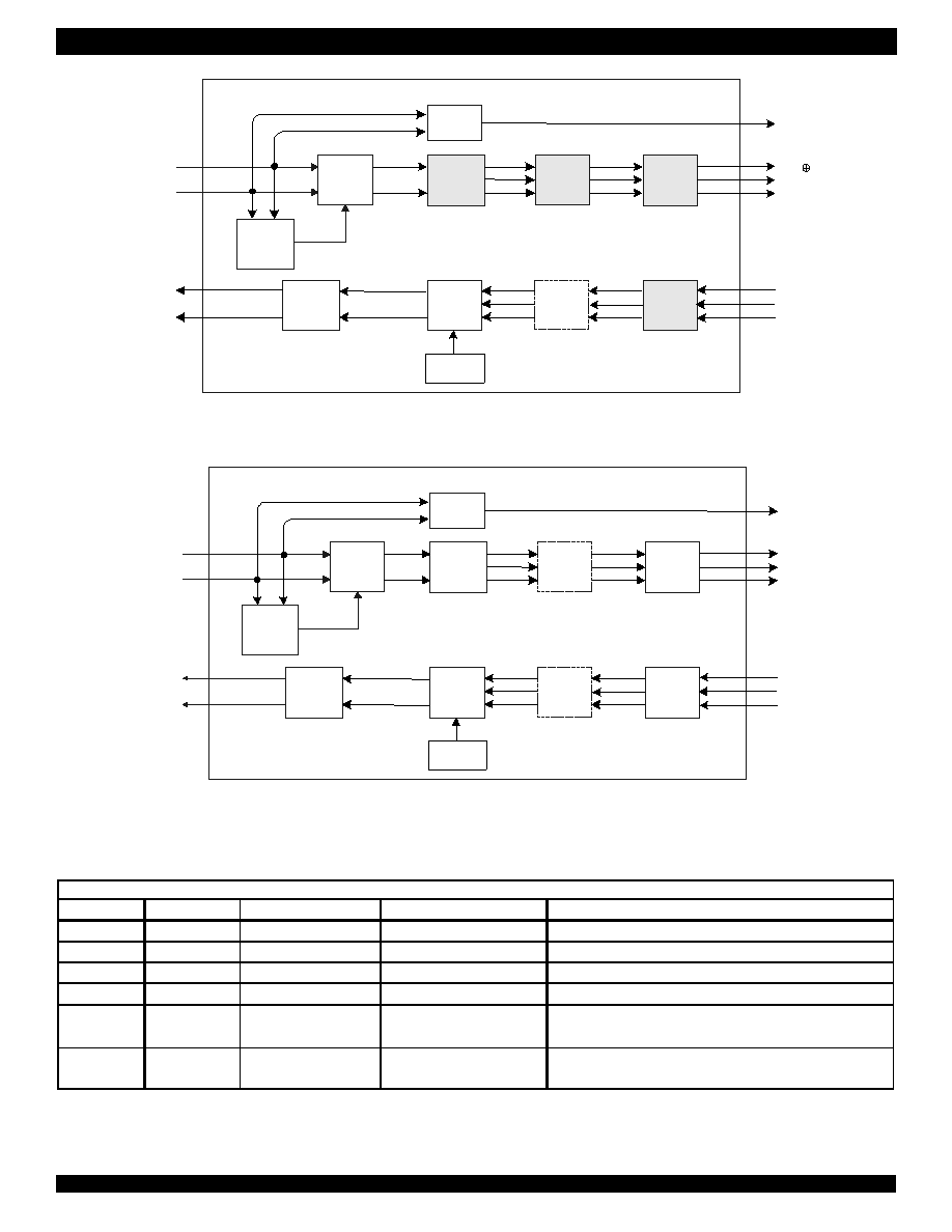
FUNCTIONAL DESCRIPTION
OVERVIEW
The IDT82V2058 is a fully integrated octal short-haul line interface
unit, which contains eight transmit and receive channels for use in E1
applications. The receiver performs clock and data recovery. As an
option, the raw sliced data (no retiming) can be output to the system.
Transmit equalization is implemented with low-impedance output driv-
ers that provide shaped waveforms to the transformer, guaranteeing
template conformance. A selectable jitter attenuation may be placed in
the receive path or the transmit path. Moreover, multiple testing func-
tions, such as error detection, loopback and JTAG boundary scan are
also provided. The device is optimized for flexible software control
through a serial or parallel host mode interface. Hardware control is
also available. Figure-1 shows One of the Eight Identical Channels
operation.
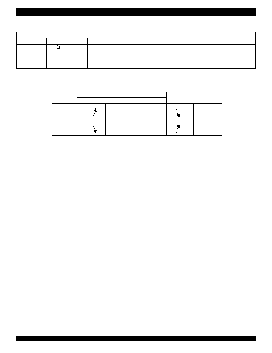
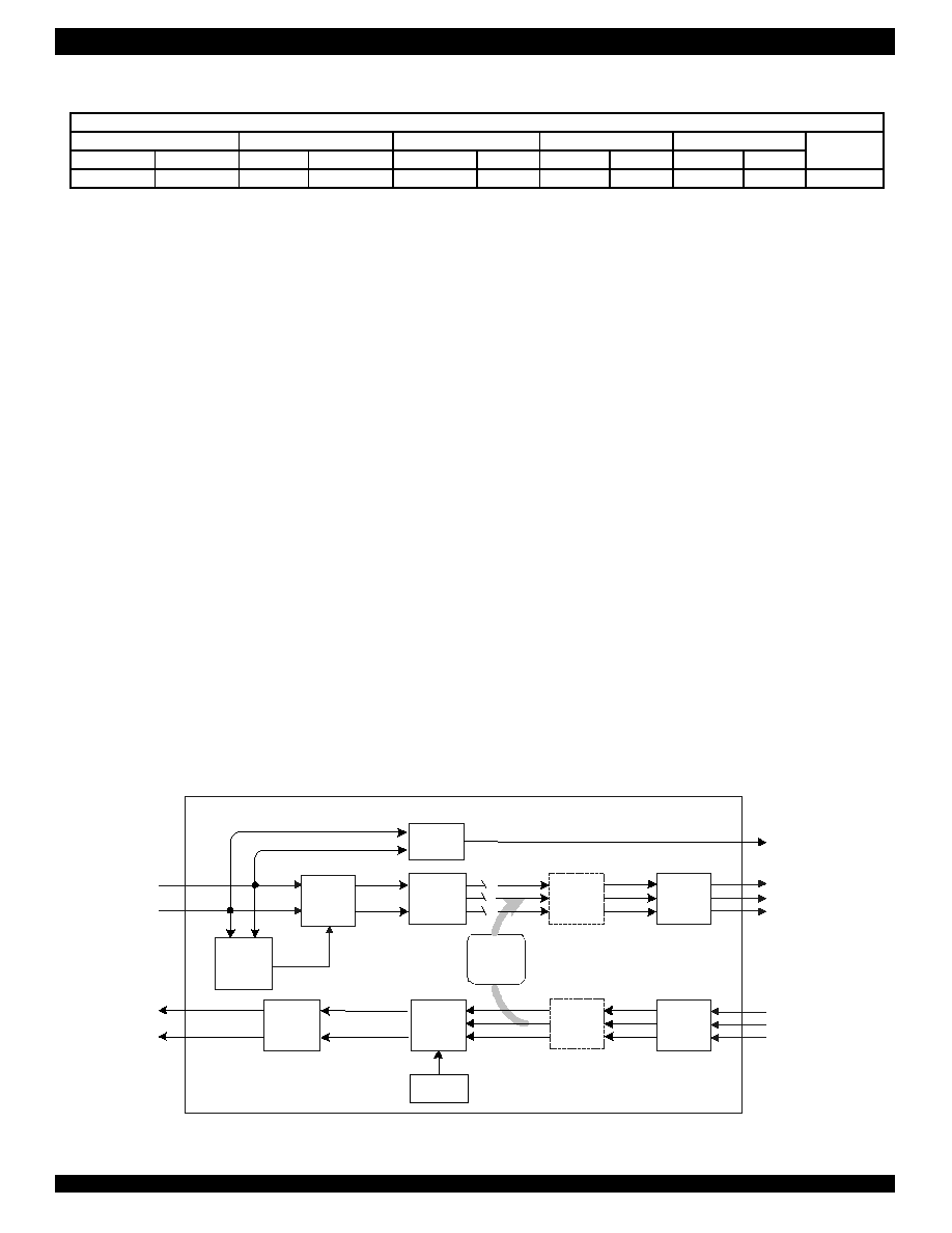
SYSTEM INTERFACE
The system interface of each channel can be configured to
operate in different modes:
1. Single Rail interface with clock recovery.
2. Dual Rail interface with clock recovery.
3. Dual Rail interface with data recovery (that is, with raw data slic-
ing only and without clock recovery).
Therefore, each signal pin on system side has multiple functions
depending on which operation mode the device is in.
Dual Rail interface consists of TDPn
1
, TDNn, TCLKn, RDPn, RDNn
and RCLKn. Data transmitted from TDPn and TDNn appears on
TTIPn and TRINGn at the line interface; data received from the RTIPn
and RRINGn at the line interface are transferred to RDPn and RDNn
while the recovered clock extracting from the received data stream
outputs on RCLKn. In Dual Rail operation, the clock/data recovery
mode is selectable. Dual Rail interface with clock recovery shown in
Figure-3 is a default configuration mode. Dual Rail interface with data
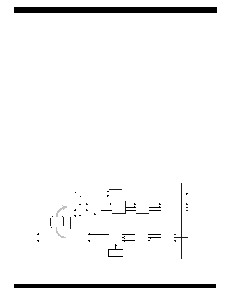
recovery is shown in Figure-4. Pin RDPn and RDNn, in this condition,
NOTE:
1. The footprint `n' (n = 0 - 7) indicates one of the eight channels
2. The first letter "e-"indicates expanded register.
3. The grey blocks are bypassed and the dotted blocks are selectable
Figure - 3. Dual Rail Interface with Clock Recovery
3
Jitter
Attenuator
Jitter
Attenuator
HDB3/
AMI
Decoder
HDB3/
AMI
Encoder
Slicer
Peak
Detector
CLK&Data
Recovery
(DPLL)
Line
Driver
Waveform
Shaper
LOS
Detector
One of Eight Identical Channels
RTIPn
RRINGn
TTIPn
TRINGn
LOSn
RCLKn
RDPn
RDNn
TCLKn
TDNn
TDPn
Transmit
All Ones
are raw RZ slice output and internally connected to an EXOR which is
fed to the RCLKn output for external clock recovery applications.
In Single Rail mode, data transmitted from TDn appears on TTIPn
and TRINGn at the line interface. Data received from the RTIPn and
RRINGn at the line interface appears on RDn while the recovered
clock extracting from the received data stream outputs on RCLKn.
When the device is in Single Rail interface, the selectable AMI or
HDB3 line encoder/decoder is available and any code violation in the
received data will be indicated at the CVn pin. The Single Rail mode
can be divided into 2 sub-modes. Single Rail mode1, whose interface
is composed of TDn, TCLKn, RDn, CVn and RCLKn, is realized by
pulling pin TDNn to high for more than 16 consecutive TCLK cycles.
Single Rail mode 2, whose interface is composed of TDn, TCLKn,
RDn, CVn, RCLKn and BPVIn, is realized by setting bit CRS in e-
CRS
2
and bit SING in e-SING. The difference between them is that, in
the latter mode bipolar violation can be inserted via pin BPVIn if AMI
line code is selected.
The configuration of different system interface is summarized in
Table-1.
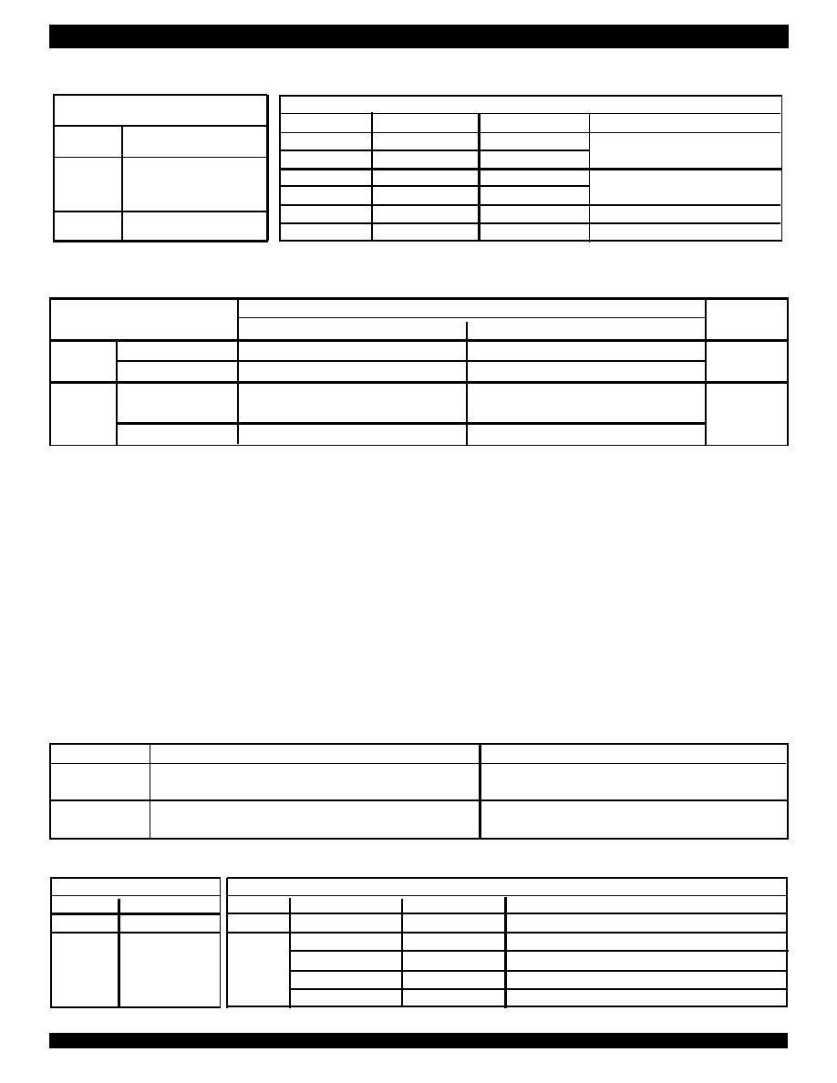
CLOCK EDGES
The active edge of RCLK and SCLK(serial interface clock) are also
selectable. If pin CLKE is Low, the active edge of RCLK is the rising
edge, as for SCLK, that is falling edge. On the contrary, if CLKE is
High, the active edge of RCLK is the falling edge and that of SCLK is
rising edge. Pins RDn/RDPn, CVn/RDNn and SDO are always active
high, and those output signals are valid on the active edge of RCLK
and SCLK respectively. See Table-2 for details. However, in dual rail
mode without clock recovery, pin CLKE is used to set the active level
for RDPn/RDNn raw slicing output: High for active high polarity and
Low for active low. It should be noted that data on pin SDI are always
active high and is sampled on the rising edge of SCLK. The data on
pin TD/TDP or BPVI/TDN are also always active high but is sampled
on the falling edge of TCLK, despite the level on CLKE.
12
INDUSTRIAL TEMPERATURE RANGES
IDT82V2058 OCTAL E1 SHORT HAUL LINE INTERFACE UNIT
Jitter
Attenuator
Jitter
Attenuator
HDB3/
AMI
Decoder
HDB3/
AMI
Encoder
Slicer
Peak
Detector
CLK&Data
Recovery
(DPLL)
Line
Driver
Waveform
Shaper
LOS
Detector
One of Eight Identical Channels
RTIPn
RRINGn
TTIPn
TRINGn
LOSn
RCLKn
RDn
CVn
TCLKn
TDNn/BPVIn
TDn
Transmit
All Ones
Figure - 6. Single Rail Mode
Figure - 4. Dual Rail Interface with Data Recovery
Jitter
Attenuator
HDB3/
AMI
Decoder
HDB3/
AMI
Encoder
Slicer
Peak
Detector
CLK&Data
Recovery
(DPLL)
Line
Driver
Waveform
Shaper
LOS
Detector
One of Eight Identical Channels
RTIPn
RRINGn
TTIPn
TRINGn
LOSn
RCLKn
(RDP RDN)
RDPn
RDNn
TCLKn
TDNn
TDPn
Transmit
All Ones
Jitter
Attenuator
Host Mode
MCLK
TDNn
CRSn in
e-CRS
SINGn in
e-SING
Interface
clocked
H
0
0
Single Rail mode 1
clocked
pulse
0
1
Single Rail mode 2
clocked
pulse
0
0
Dual Rail with Clock Recovery
clocked
pulse
1
0
Dual Rail with Data Recovery
H
pulse
-
-
Receive just slice the incoming data.
Transmit is determined by the status of TCLKn.
L
pulse
-
-
Receive is power down.
Transmit is determined by the status of TCLKn.
TABLE - 1a. SYSTEM INTERFACE CONFIGURATION (Host Mode)
13
INDUSTRIAL TEMPERATURE RANGES
IDT82V2058 OCTAL E1 SHORT HAUL LINE INTERFACE UNIT
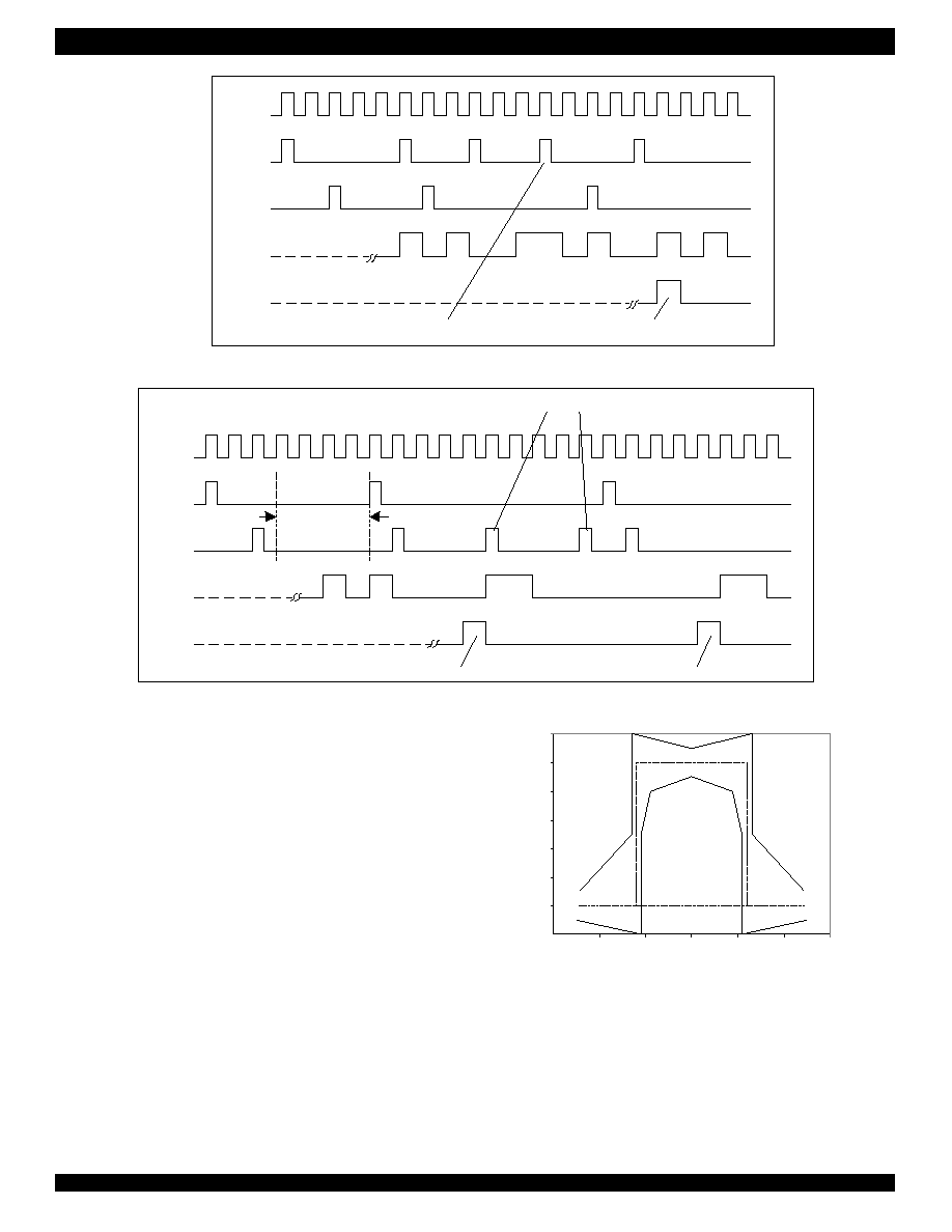
RECEIVER
In receive path, the line signals couple into RRINGn and RTIPn via
a transformer and are converted into RZ digital pulses by a data
slicer. Adaptation for attenuation is achieved using an integral peak
detector that sets the slicing levels. Clock and data are recovered
from the received RZ digital pulses by a digital phase-locked loop that
provides excellent jitter accommodation. After passing through the
selectable jitter attenuator, the recovered data are decoded using
HDB3 or AMI line code rules and clocked out of pin RDn in single rail
mode, or presented on RDPn/RDNn in an undecoded dual rail NRZ
format. Loss of signal, alarm indication signal, line code violations and
excessive zero are detected. These various changes in status may
be enabled to generate interrupts.
Peak Detector and Slicer
The slicer determines the presence and polarity of the received
pulses. In data recovery mode, the raw positive slicer output appears
on RDPn while the negative slicer output appears on RDNn. In clock
and data recovery mode, the slicer output is sent to Clock and Data
Recovery circuit for abstracting retimed data and optional decoding.
The slicer circuit has a built-in peak detector from which the slicing
threshold is derived. The slicing threshold is default to 50% (typical) of
the peak value.
Signals with an attenuation of up to 12 dB (from 2.4V) can be re-
covered accurately by the receiver. To provide immunity from impul-
sive noise, the peak detectors are held above a minimum level of
0.150 V typically, despite the received signal level.
Clock and Data Recovery
The function of Clock and Data Recovery is accomplished by
Digital Phase Locked Loop (DPLL). The DPLL is clocked 16 times of
the received clock rate, i.e. 32.768 MHz in E1 mode. The recovered
data and clock from DPLL is then sent to the selectable Jitter
Attenuator or decoder circuit for further processing.
RD/RDP and CV/RDN
Pin CLKE
Clock recovery
Slicer output
SDO
Low
RCLK
Active High
Active Low
SCLK Active High
High
RCLK
Active High
Active High
SCLK
Active High
TABLE - 2. ACTIVE CLOCK EDGE AND ACTIVE LEVEL
The clock recovery and data recovery mode can be selected on
per channel basis by setting the bit CRSn in e-CRS. When bit CRSn is
defaulted to `0', the corresponding channel operates in data and clock
recovery mode. The recovered clock is output on pin RCLKn and re-
timed NRZ data are output on pin RDPn/RDNn in dual rail mode or on
RDn in single rail mode. When CRSn is `1', dual rail with data
recovery mode is enabled in the corresponding channel and the clock
recovery function is bypassed. In this condition, the analog line signal
are converted to RZ digital bit streams on the RDPn/RDNn pins and
internally connected to an EXOR which is fed to the RCLKn output for
external clock recovery applications.
Moreover, Pulling MCLK to H level, all the receivers will enter the
dual rail with data recovery mode. In this case, e-CRS is ignored.
HDB3/AMI Line Code Rule
Selectable HDB3 or AMI line coding/decoding is provided when the
device is configured in single rail mode. HDB3 rules is enabled by set-
ting bit CODE in register GCF (global control configuration) to `0' or
pulling pin CODE to Low. AMI rule is enabled by setting bit CODE in
GCF to `1' or pulling pin CODE to High. All the setting above are ef-
fected to eight channels.
Individual line code rule selection for each channel, if need, is
available by setting bit SINGn in e-SING to `1' (to activate bit CODEn in
e-CODE) and programming bit CODEn to select line code rules in the
corresponding channel: `0' for HDB3, while `1' for AMI. In this case, the
value in bit CODE in GCF or pin CODE for global control is unaffected
in the corresponding channel and only affect in other channels.
In dual rail mode, the decoder/encoder are bypassed. Bit CODE in
GCF, bit CODEn in e-CODE and pin CODE are ignored.
The configuration of the Line Code Rule is summarized in Table-3.
TABLE - 1b. SYSTEM INTERFACE CONFIGURATION (Hardware Mode)
Hardware Mode
MCLK
TDNn
Interface
clocked
H ( 16 MCLK)
Single Rail mode 1
clocked
pulse
Dual Rail with Clock Recovery
H
pulse
Receive just slice the incoming data. Transmit is determined by the status of TCLKn.
L
pulse
Receive is power down. Transmit is determined by the status of TCLKn.
14
INDUSTRIAL TEMPERATURE RANGES
IDT82V2058 OCTAL E1 SHORT HAUL LINE INTERFACE UNIT
TABLE - 5. AIS CONDITION
TABLE - 4. LOS CONDITION IN CLOCK RECOVERY MODE
TABLE - 3. CONFIGURATION OF THE LINE CODE RULE
Loss of Signal (LOS) Detection
The Loss of Signal Detector monitors the amplitude and density of
the received signal on Receiver line before the transformer
(measured on port A, B in Figure 12). The loss condition is reported
by pulling pin LOSn to high. In the same time, LOS alarm registers
track LOS condition. When LOS detected or cleared, an interrupt will
generate if not masked. In host mode, the detection supports the ITU-
G.775 and ETSI 300233. In hardware mode, it only supports the ITU-
G.775 specification.
Table-4 summarizes the conditions of LOS in clock recovery
mode.
In data recovery mode, the LOS condition is cleared upon
detecting the signal level exceeds 540mV.
During LOS, the RDPn/RDNn output the sliced data when bit
AISE(Alam Indication Signal Enable) in register GCF is 0 or output all
ones as AIS (Alarm Indication Signal) when bit AISE is set to 1; The
RCLKn is replaced by MCLK only if the AISE is set.
Alarm Indication Signal Detection (AIS)
Alarm Indication Signal is available only in host mode with clock
recovery, as Table-5 shows.
Error Detection
The device can detects excessive zero, bipolar violations and
HDB3 code violations, refer to figure-7, 8, 9. All the three kinds of er-
rors are reported in both host mode and hardware mode with HDB3
line code rule is used. Moreover, in host mode, the expanded regis-
ters e-CZER and e-CODV are used to determine whether the exces-
TABLE - 6. ERROR DETECTION
STANDARD Signal on
G.775 for E1
ETSI 300233 for E1 pin LOSn
LOS
Continuous Intervals
32
2048 (1 ms)
H
Detected
Amplitude
below typ. 310mV (Vpp)
below typ. 310mV (Vpp)
LOS
Density
12.5% (4 marks in a sliding 32-bit period)
12.5% (4 marks in a sliding 32-bit period)
L
Cleared
with no more that 15 continuous zeros
with no more than 15 continuous zeros
Amplitude
exceed typ. 540mV (Vpp)
exceed typ. 540mV (Vpp)
ITU G.755 for E1 (register LAC defaulted to 0)
ETSI 300233 for E1 (register LAC is 1)
AIS Detected
Less than 3 zeros contained in each of two consecutive
Less than 3 zeros contained in a 512-bit stream
512-bit stream are received
are received
AIS Cleared
3 or more zeros contained in each of two consecutive
3 or more zeros contained in a 512-bit stream
512-bit stream are received
are received
Hardware Mode
Host Mode
Line Code
Pin CVn Reports
Line Code CODVn in
e-CODV CZERn in e-CZER
Pin CVn Reports
AMI
Bipolar Violation
AMI
-
-
Bipolar Violation
HDB3
Bipolar Violation
HDB3
0
0
Bipolar Violation + Code Violation
+ Code Violation
0
1
Bipolar Violation + Code Violation + Excessive Zero
+ Excessive Zero
1
0
Bipolar Violation
1
1
Bipolar Violation + Excessive Zero
Host Mode
CODE in
GCF CODEn in e-CODE SINGn in e-SINGn
Line Code Rule
0
0 / 1
0
All channels in HDB3
0
0
1
1
0 / 1
0
All channels in AMI
1
1
1
0
1
1
CHn in AMI
1
0
1
CHn in HDB3
Hardware Mode
CODE
Line Code Rule
L
All channels in HDB3
H All channels in AMI
15
INDUSTRIAL TEMPERATURE RANGES
IDT82V2058 OCTAL E1 SHORT HAUL LINE INTERFACE UNIT
-300
-200
-100
0
100
200
300
Time (ns)
-0.20
0.00
0.20
0.40
0.60
0.80
1.00
1.20
Normalized Amplitude
Figure - 9. CEPT Waveform Template
sive zero and code violation are reported respectively. When
configured in AMI decoding mode, only bipolar violation can be re-
ported.
The error detection is available only in single rail mode where the
pin RDNn/CVn is used as error report output (CVn pin).
The configuration and report status of error detection are summa-
rized in Table-6.
TRANSMITTER
In transmit path, data in NRZ (non return to zero) format are
clocked into the device on TDn and encoded by AMI or HDB3 line
code rules when single rail mode is configured or pre-encoded data
in NRZ format are input on TDPn and TDNn when dual rail mode is
configured. The data are sampled into the device on falling edges of
TCLKn. Jitter attenuator, if enabled, is provided with a FIFO which the
data to be transmitted are passing through. A low jitter clock is
generated by an integral digital phase-locked loop and is used to
read data from the FIFO. The shape of the pulses should meet the
E1 pulse template after the signal is passed through different cable
types. Bipolar violation, for diagnosing, can be inserted on pin BPVIn
if AMI line code rule is enabled.
Waveform Shaper
E1 pulse template, specified in ITU-T G.703, is shown in Figure-9.
The device has built-in transmit waveform templates for cable of 75
or 120
.
The built-in waveform shaper use an internal high frequency clock
which is 16XMCLK as clock reference. This function will be bypassed
when MCLK is unavailable.
Figure - 7. AMI Bipolar Violation
Bipolar Violation detected
Bipolar violation
CLK
RTIP
RRING
RD
CV
1
2
3
4
5
V
6
7
1
2
3
4
5
6
V
Figure - 8. HDB3 Code Violation & Excessive Zero
Code violation detected
Excessive zero detected
CLK
RTIP
RRING
RD
CV
Code violation
4 consecutive zeros
1
2
3
4
V
V
5
6
1
2
3
4
5
6
16
INDUSTRIAL TEMPERATURE RANGES
IDT82V2058 OCTAL E1 SHORT HAUL LINE INTERFACE UNIT
Bipolar Violation Insertion
When configured in single rail mode 2 with AMI line code enabled,
pin TDNn/BPVIn is used as BPVI input. A low-to-high transition on this
pin inserts a bipolar violation on the next available mark in the trans-
mit data stream. Sampling occurs on the falling edge of TCLK. But in
TAOS with analog loopback mode and remote loopback mode, the
BPVI is disabled. In TAOS with digital loopback mode, the BPVI is
looped back to system side, so
the data to be transmitted
on TTINGn
and TRINGn are all ones with no bipolar violation.
JITTER ATTENUATOR
The jitter attenuator is provided for narrow-band width jitter transfer
and can be selected to work either in transmit path or in receive path
or not used. The selection is accomplished by setting pin JAS in hard-
ware mode or configuring bits JACF1 and JACF0 in register GCF in
host mode which are both effected to all the channels.
For applications which require line synchronization, the line clock
is need to be extracted for the internal synchronization, the jitter
attenuator is set in the receive path. Another use of the jitter attenuator
is to provide clock smoothing in the transmit path for applications such
as synchronous/asynchronous demultiplexing applications. In these
applications, TCLK will have an instantaneous frequency that is higher
than the nominal E1 data rate and in order to set the average long-
term TCLK frequency within the transmit line rate specifications, peri-
ods of TCLK are suppressed (gapped).
The jitter attenuator integrates a FIFO which can accommodate a
gapped TCLK. In host mode, the FIFO length can be 32 X 2 or 64 X 2
bits by programming bit JADP in GCF. In hardware mode, it is fixed to
64 X 2 bits. The FIFO length determines the maximum permissible
gap width (see table-7), exceeding these values will cause FIFO over-
flow or underflow. The data is 16 or 32 bits' delay through the jitter
FIFO Length
Max. Gap Width
64 bit
56 UI
32 bit
28 UI
TABLE - 7. GAP WIDTH LIMITATION
attenuator in the corresponding transmit or receive path. The constant
delay feature is crucial for the applications requiring "hitless" switching.
In host mode, bit JABW in GCF determines the jitter attenuator 3dB
corner frequency (fc). In hardware mode, the fc is fixed to 1.7Hz.
Generally, the lower the fc is, the higher the attenuation. However,
lower fc comes at the expense of increased acquisition time.
Therefore, the optimum fc is to optimize both the attenuation and the
acquisition time. In addition, the longer FIFO length results in an
increased throughput delay and also influences the 3dB corner
frequency. Generally, it's recommended to use the lower corner
frequency and the shortest FIFO length that can still meet jitter
attenuation requirements.
The output jitter specifications include: ITU-T G.736, ITU-T G.742,
ITU-T G.783 and ETSI CTR 12/13.
Figure - 10. External Transmit/Receive Line Circuitry
0.22
µ
F
∑
∑
∑
∑ ∑
R
X
Line
1k
R
R
R
R
∑
∑
T
X
Line
R
T
R
T
RTIPn
RRINGn
TRINGn
TTIPn
∑
∑
0.1
µ
F
GNDTn
VDDDn
VDDT
IDT82V2058
One of Eight Identical Channels
VDDT
∑
∑
VDDT
D4
D3
D2
D1
2:1
1
2:1
1
1k
Cp
2
68
µ
F
3
A
B
NOTE:
1. Pulse T1124 transformer is recommended to use in Standard (STD) operating temperature range (0∞ to 70∞C), while Pulse T1114 transformer is recommended to use in Extended (EXT)
operating temperature range is -40∞ to +85∞C. See Transformer Specifications Table for details.
2. Typical value. Adjust for actual board parasitics to obtain optimum return loss.
3. Common decoupling capacitor for all VDDT and GNDT pins.
Component
75
Coax
120
Twisted Pair
R
T
9.5
±
1%
9.5
±
1%
R
R
9.31
±
1%
15
±
1%
Cp
2200pf
D1 ≠ D4
Nihon Inter Electronics - EP05Q03L, 11EQS03L,
EC10QS04, EC10QS03L
Motorola ≠ MBR0540T1
TABLE - 8. EXTERNAL COMPONENTS VALUES
17
INDUSTRIAL TEMPERATURE RANGES
IDT82V2058 OCTAL E1 SHORT HAUL LINE INTERFACE UNIT
Jitter
Attenuator
Jitter
Attenuator
HDB3/AMI
Decoder
HDB3/AMI
Encoder
Slicer
Peak
Detector
CLK&Data
Recovery
(DPLL)
Line
Driver
Waveform
Shaper
LOS
Detector
Digital
Loopback
One of Eight Identical Channels
RTIPn
RRINGn
TTIPn
TRINGn
LOSn
RCLKn
RDn/RDPn
CVn/RDNn
TCLKn
BPVIn/TDNn
TDn/TDPn
Transmit
All Ones
Figure - 11. Digital Loopback
LINE INTERFACE CIRCUITRY
The transmit and receive interface RTIP/RRING and TTIP/TRING
connections provide a matched interface to the cable. Figure-12
shows the appropriate external components to connect with the cable
for one transmit/receive channel. Table-8 summarizes the
component values based on the specific application.
TRANSMIT DRIVER POWER SUPPLY
The nominal transmit driver power supply must be 5.0V or 3.3V.
Despite of the power supply voltage, the 75
/120
lines are
driven through 9.5
series resistors and a 1:2 transformer.
However, in harsh cable environment, series resistors are re-
quired to improve the transmit return loss performance and protect
the device from surges coupling into the device.
SHORT CIRCUIT MONITOR
An internal Short Circuit Monitor (SCM), parallelly connected with
TTIPn and TRINGn, can detect short circuit in the transmit line side.
Bit SCPB in Register GCF decides whether the output driver short-
circuit protection is enabled. (Refer to
Programming Information).
When it is enabled, the max driver's output current is limited to
150mA.
LINE PROTECTION
In transmit side, the Schottky diodes D1~D4 are required to protect
the line driver and improve the design robustness. In receive side,
the series resistors of 1k
are used to protect the receiver against
current surges coupled in the device. It does not affect the receiver
sensitivity, since the receiver impedance is as high as 120k
typi-
cally.
HITLESS PROTECTION SWITCHING (HPS)
The IDT82V2048 tranceivers include an output driver tristatability
feature for T1/E1 redundancy applications. This feature greatly re-
duces the cost of implementing redundancy protection by eliminating
external relays. Details of HPS will be described in relative Application
Note.
RESET
Writing register RS can cause software reset by initiating about 1
µ
s
reset cycle. This operation set all the registers to their default value.
POWER UP
During power up, an internal reset signal sets all the registers to
default values. This procedure takes at least 2 machine cycles.
POWER DOWN
Each transmitter channel will power down by pulling pin TCLKn to
low for more than 64 MCLK cycles (if MCLK is available) or about
30us (when MCLK is not availabe). Each transmitter channel will also
power down by setting bit TPDNn in e-TPDN to 1.
All the receivers will power down when MCLK is Low. When MCLK
is clocked or High, setting bit RPDNn in e-RPDN to `1' will configure the
corresponding receiver to power down.
INTERFACE WITH 5V LOGIC
The IDT82V2048 can interface directly with 5V TTL family devices.
The internal input pads are tolerant to 5V output from TTL and CMOS
family devices.
Electrical Specification @ 25 ∞C
Part No.
Turns Ratio
(Pri: sec±2%)
OCL @ 25∞C
(mH MIN)
L
L
(
µ
H MAX)
C
W/W
(pF MAX)
STD Temp.
EXT Temp.
Transmit
Receive
Transmit
Receive
Transmit
Receive
Transmit
Receive
Package/
Schematic
T1124
T1114
1:2CT
1CT:2
1.2
1.2
.6
.6
35
35
TOU/3
TABLE - 9. TRANSFORMER SPECIFICATIONS
18
INDUSTRIAL TEMPERATURE RANGES
IDT82V2058 OCTAL E1 SHORT HAUL LINE INTERFACE UNIT
LOOPBACK MODE
The device provides four different diagnostic loopback configura-
tions: Digital Loopback, Analog Loopback, Remote Loopback and
Dual Loopback. In host mode, these functions are implemented by
programming the registers DLB, ALB or RLB. In hardware mode,
only analog loopback and remote loopback can be selected by pull-
ing pin LPn to High and Low respectively.
Digital Loopback
By programming the bits of register DLB, each channel of the de-
vice can be set in Local Digital Loopback. In this configuration, the
data and clock to be transmitted, after passing the encoder, is looped
back to jitter attenuator (if enabled) and decoder in the receive path,
then output on RCLKn, RDn/RDPn and CVn/RDNn. The data to be
transmitted are still output on TTIPn and TRINGn while the data re-
ceived on RTIPn and RRINGn are ignored. The Loss Detector is still
in use. Figure-11 shows the process.
Analog Loopback
By programming the bits of ALB register or pulling pin LPn to
High, each channel of the device can be set in Analog Loopback. In
this configuration, the data to be transmitted output from the line driver
are internally looped back to the slicer and peak detector in the
receive path and output on RCLKn, RDn/RDPn and CVn/RDNn. The
data to be transmitted are still output on TTIPn and TRINGn while the
data received on RTIPn and RRINGn are ignored. The Loss Detector
is still in use. Figure-12 shows the process.
The TTIPn and RTIPn, TRINGn and RRINGn cannot be connected
directly to do the external analog loopback test. Line impedance
loading is required to conduct the external analog loopback test.
Remote Loopback
By programming the bits of RLB register or pulling pin LPn to Low,
each channel of the device can be set in Remote Loopback. In this
configuration, the data and clock recovered by the Clock and Data
Recovery circuits are looped to waveform shaper and output on
TTIPn and TRINGn. The jitter attenuator is also included in loopback
when enabled in the transmit or receive path. The received data and
clock are still output on RCLKn, RDn/RDPn and CVn/RDNn while the
data to be transmitted on TCLKn, TDn/TDPn and BPVIn/TDNn are
ignored. The Loss Detector is still in use. Figure-13 shows the
process.
Dual Loopback
Dual Loopback mode is set by setting both bit DLBn in register
DLB and bit RLBn in register RLB to `1'. In this configuration, after
passing the encoder, the data and clock to be transmitted are looped
back to decoder directly and output on RCLKn, RDn/RDPn and CVn/
RDNn. The recovered data from RTIPn and RRINGn are looped back
to waveform shaper through JA (if selected) and output on TTIPn and
TRINGn. The Loss Detector is still in use. Figure-14 shows the proc-
ess.
Transmit All Ones
In hardware mode, the TAOS mode is set by pulling TCLKn High
for more than 16 MCLK cycles. In host mode, TAOS mode is set by
programming register TAO. In addition, automatic TAO signals are in-
serted by setting register ATAO when Loss of Signal occurs. Note that
the TAOS generator adopts MCLK as a timing reference. In order to
assure that the output frequency is within specification limits, MCLK
must have the applicable stability.
This TAOS mode and Digital Loopback or Analog Loopback can
be configured simultaneously. Figure-15 shows their process.
Figure - 12. Analog Loopback
Jitter
Attenuator
Jitter
Attenuator
HDB3/AMI
Decoder
HDB3/AMI
Encoder
Analog
Loopback
Slicer
Peak
Detector
CLK&Data
Recovery
(DPLL)
Line
Driver
Waveform
Shaper
LOS
Detector
One of Eight Identical Channels
RTIPn
RRINGn
TTIPn
TRINGn
LOSn
RCLKn
RDn/RDPn
CVn/RDNn
TCLKn
BPVIn/TDNn
TDn/TDPn
Transmit
All Ones

19
INDUSTRIAL TEMPERATURE RANGES
IDT82V2058 OCTAL E1 SHORT HAUL LINE INTERFACE UNIT
Figure - 15a. TAOS Data Path
Jitter
Attenuator
Jitter
Attenuator
HDB3/AMI
Decoder
HDB3/AMI
Encoder
Slicer
Peak
Detector
CLK&Data
Recovery
(DPLL)
Line
Driver
Waveform
Shaper
LOS
Detector
One of Eight Identical Channels
RTIPn
RRINGn
TTIPn
TRINGn
LOSn
RCLKn
RDn/RDPn
CVn/RDNn
TCLKn
BPVIn/TDNn
TDn/TDPn
Transmit
All Ones
Figure - 13. Remote Loopback
Jitter
Attenuator
Jitter
Attenuator
HDB3/AMI
Decoder
HDB3/AMI
Encoder
Remote
Loopback
Slicer
Peak
Detector
CLK&Data
Recovery
(DPLL)
Line
Driver
Waveform
Shaper
LOS
Detector
One of Eight Identical Channels
RTIPn
RRINGn
TTIPn
TRINGn
LOSn
RCLKn
RDn/RDPn
CVn/RDNn
TCLKn
BPVIn/TDNn
TDn/TDPn
Transmit
All Ones
Jitter
Attenuator
Jitter
Attenuator
HDB3/AMI
Decoder
HDB3/AMI
Encoder
Slicer
Peak
Detector
CLK&Data
Recovery
(DPLL)
Line
Driver
Waveform
Shaper
LOS
Detector
One of Eight Identical Channels
RTIPn
RRINGn
TTIPn
TRINGn
LOSn
RCLKn
RDn/RDPn
CVn/RDNn
TCLKn
BPVIn/TDNn
TDn/TDPn
Transmit
All Ones
Figure - 14. Dual Loopback

20
INDUSTRIAL TEMPERATURE RANGES
IDT82V2058 OCTAL E1 SHORT HAUL LINE INTERFACE UNIT
HOST INTERFACES
The host interface provides access to read and write the registers
in the device. The interface consists of serial host interface and
parallel host interface. By pulling pin MODE2 to VDDIO/2 or to High,
the device can be set to work in serial mode and in parallel mode
respectively.
Parallel Host Interface
The interface is compatible with Motorola or Intel host. Pins
MODE1 and MODE0 are used to select the operating mode of the
parallel host interface. When pin MODE1 is pulled to Low, the host
uses separate address bus and data bus. When High, multiplexed
address/data bus is used. When pin MODE0 is pulled to Low, the par-
allel host interface is configured for Motorola compatible hosts. When
High, for Intel compatible hosts. This is well described in the
Pin De-
scription. The host interface pins in each operation mode is tabu-
lated in Table-10.
Jitter
Attenuator
Jitter
Attenuator
HDB3/AMI
Decoder
HDB3/AMI
Encoder
Slicer
Peak
Detector
CLK&Data
Recovery
(DPLL)
Line
Driver
Waveform
Shaper
LOS
Detector
One of Eight Identical Channels
RTIPn
RRINGn
TTIPn
TRINGn
LOSn
RCLKn
RDn/RDPn
CVn/RDNn
TCLKn
BPVIn/TDNn
TDn/TDPn
Transmit
All Ones
Figure - 15c. TAOS with Analog Loopback
Jitter
Attenuator
HDB3/AMI
Decoder
HDB3/AMI
Encoder
Slicer
Peak
Detector
CLK&Data
Recovery
(DPLL)
Line
Driver
Waveform
Shaper
LOS
Detector
One of Eight Identical Channels
RTIPn
RRINGn
TTIPn
TRINGn
LOSn
RCLKn
RDn/RDPn
CVn/RDNn
TCLKn
BPVIn/TDNn
TDn/TDPn
Transmit
All Ones
Figure - 15b. TAOS with Digital Loopback
Serial Host Interface
By pulling pin MODE2 to VDDIO/2, the device operates in the serial
host Mode. In this mode, the registers are accessible through a 16-bit
word which contains an 8-bit command/address byte (bit R/W and 5-ad-
dress-bit A1~A5, A6 and A7 are ignored) and a subsequent 8-bit data
byte (D0~D7). When bit R/W is 1, data is read out at pin SDO. When bit
R/W is 0, data is written into pin SDI to the register which is indicated by
address bits A5~A1.
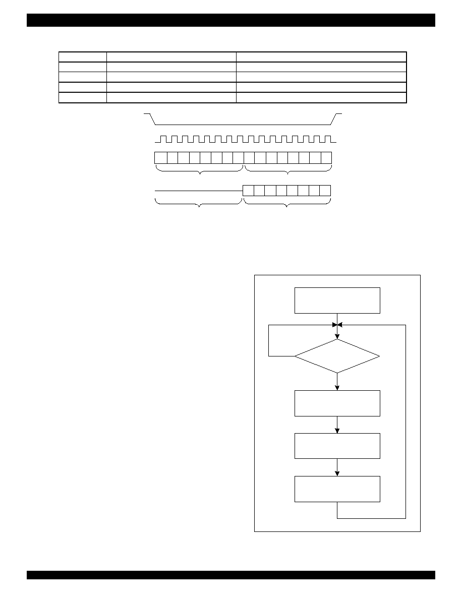
INTERRUPT HANDLING
Interrupt Sources
There are three kinds of interrupt sources:
1. Status change in the LOS (Loss of Signal) Status Register(04H).
The analog/digital loss of signal detector continuously monitors the re-
ceived signal to update the specific bit in LOS which indicates presence
or absence of a LOS condition.
21
INDUSTRIAL TEMPERATURE RANGES
IDT82V2058 OCTAL E1 SHORT HAUL LINE INTERFACE UNIT
Service the Interrupt
Read Interrupt Status Register
Read Corresponding Status
Register
Interrupt Allowed
Interrupt Condition
Exist?
Yes
No
Figure - 17. Interrupt Service Routine
2. Status change in the SC (Short Circuit) Status Register(05H).
The automatic power driver circuit continuously monitors the output
drivers signal to update the specific bit in SCM which indicates pres-
ence or absence of the transmit line side short circuit condition.
3. Status change in the AIS (Alarm Indication Signal) Status
Register(13H). The AIS detector monitors the received signal to up-
date the specific bit in AIS which indicates presence or absence of a
AIS condition.
Interrupt Enable
The IDT82V2058 provides a latched interrupt output (INT) and the
three kinds of interrupts are all reported by this pin. When the Interrupt
Mask register (LOSM , SCM and AISM) is set to `1', the Interrupt Sta-
tus register (LOSI, SCI and AISI) is enabled respectively. Whenever
there is a transition (`0' to `1' or `1' to `0') in the corresponding Status
register, the Interrupt Status register will change into `1', which means
an interrupt occurs, and there will be a transition from high to low on
INT. An external pull-up resistor of approximately 10k
is required to
support the wire-OR operation of INT. When any of the three Interrupt
Mask registers is set to `0' (the power-on default value is `0'), the cor-
responding Interrupt Status register is disabled and the transition on
status register is ignored.
Interrupt Clearing
When an interrupt occurs, the Interrupt Status registers (LOSI, SCI
and AISI) are read to identify the interrupt source. And these registers
will be cleared to `0' after the corresponding Status register (LOS, SC
and AIS) being read. The Status registers will be cleared once the
corresponding conditions are met.
Pin INT is pulled High when there are no pending interrupt left.
The interrupt handling in the interrupt service routine is showed Fig-
ure-17.
A1
A3
A2
A4 A5 A6
D0 D1 D2 D3 D4 D5 D6 D7
R/W
D0 D1 D2 D3 D4 D5 D6 D7
A7
Input Data Byte
Address/Command Byte
High Impedance
Driven while R/W=1
SDI
SDO
SCLK
CS
1
2
2
MODE[2:0]
Host interface
Generic control, data, and output pin name
100
Non-multiplexed Motorola interface
CS, ACK, DS, R/W, AS, A[4:0], D[7:0], INT
101
Non-multiplexed Intel interface
CS, RDY, WR, RD, ALE, A[4:0], D[7:0], INT
110
Multiplexed Motorola interface
CS, ACK, DS, R/W, AS, AD[7:0], INT
111
Multiplexed Intel interface
CS, RDY, WR, RD, ALE, AD[7:0], INT
TABLE - 10. PARALLEL HOST INTERFACE PINS
Figure - 16. Serial Host Mode Timing
NOTE:
1. While R/W=1, read from IDT82V2058; While R/W=0, write to IDT82V2058.
2. Ignored.

22
INDUSTRIAL TEMPERATURE RANGES
IDT82V2058 OCTAL E1 SHORT HAUL LINE INTERFACE UNIT
Jitter
Attenuator
Jitter
Attenuator
HDB3/
AMI
Decoder
HDB3/
AMI
Encoder
Slicer
Peak
Detector
CLK&Data
Recovery
(DPLL)
Line
Driver
Waveform
Shaper
LOS
Detector
Channel N ( 7 > N > 1 )
RTIPn
RRINGn
TTIPn
TRINGn
LOSn
RCLKn
RDn/RDPn
CVn/RDNn
TCLKn
BPVIn/TDNn
TDn/TDPn
G.772
Monitor
Transmit
All Ones
Jitter
Attenuator
Jitter
Attenuator
HDB3/
AMI
Decoder
HDB3/
AMI
Encoder
Remote
Loopback
Slicer
Peak
Detector
CLK&Data
Recovery
(DPLL)
Line
Driver
Waveform
Shaper
LOS
Detector
Channel 0
LOS0
RCLK0
RD0/RDP0
CV0/RDN0
TCLK0
BPVI0/TDN0
TD0/TDP0
Transmit
All Ones
RTIP0
RRING0
TTIP0
TRING0
Figure - 17. Monitoring Principle
G.772 MONITORING
The eight channels of IDT82V2058 can all be configured to work as
regular transceivers. In applications using only seven channels
(channels 1 to 7), channel 0 is configured to non-intrusively monitor
any of the other channels' inputs or outputs on the line side. The
monitoring is non-intrusive per ITU-T G.772. Figure-17 shows the
Monitoring Principle. The receiver or transmitter path to be monitored
is configured by pin MC[0:3] in hardware mode or by PMON in host
mode (refer to
Programming Information for details).
The signal which is monitored goes through the clock and data
recovery circuit of channel 0. The monitored clock can output on
RCLK0 which can be used as a timing interfaces derived from E1
signal. The monitored data can be observed digitally at the output pin
RCLK0, RD0/RDP0 and RDN0. LOS detector is still in use in channel
0 for the monitored signal.
In monitoring mode, channel 0 can be configured to the Remote
Loopback. The signal which is being monitored will output on TTIP0
and TRING0. The output signal can then be connected to a standard
test equipment with an E1 electrical interface for non-intrusive
monitoring.
23
INDUSTRIAL TEMPERATURE RANGES
IDT82V2058 OCTAL E1 SHORT HAUL LINE INTERFACE UNIT
PROGRAMMING INFORMATION
REGISTER LIST AND MAP
There are 21 primary registers (including an Address Pointer Con-
trol Register), including 8 expanded registers in the device.
Whatever the control interface is, 5 address bits are used to set the
registers. In non-multiplexed parallel interface mode, the five dedicated
address bits are A[4:0]. In multiplexed parallel interface mode, AD[4:0]
Address
Hex
serial
interface
A7-A1
parallel
interface
A7-A0
Register
R/W
Explanation
00
XX00000
XXX00000 ID
R
Device ID Register
01
XX00001
XXX00001 ALB
R/W Analog Loopback Configuration Register
02
XX00010
XXX00010 RLB
R/W Remote Loopback Configuration Register
03
XX00011
XXX00011 TAO
R/W Transmit All One Code Configuration Register
04
XX00100
XXX00100 LOS
R
Loss of Signal Status Register
05
XX00101
XXX00101 SC
R
Short Circuit Status Register
06
XX00110
XXX00110 LOSM
R/W LOS Interrupt Mask Register
07
XX00111
XXX00111 SCM
R/W Short Circuit Interrupt Mask Register
08
XX01000
XXX01000 LOSI
R
LOS Interrupt Status Register
09
XX01001
XXX01001 SCI
R
Short Circuit Interrupt Status Register
0A
XX01010
XXX01010 RS
W
Software Reset Register
0B
XX01011
XXX01011 PMON
R/W Performance Monitor Configuration Register
0C
XX01100
XXX01100 DLB
R/W Digital Loopback Configuration Register
0D
XX01101
XXX01101 LAC
R/W LOS/AIS Criteria Configuration Register
0E
XX01110
XXX01110 ATAO
R/W Automatic TAO Configuration Register
0F
XX01111
XXX01111 GCF
R/W Global Configuration Register
10
XX10000
XXX10000
11
XX10001
XXX10001
Reserved
12
XX10010
XXX10010 OE
R/W Output Enable Configuration Register
13
XX10011
XXX10011 AIS
R
AIS Status Register
14
XX10100
XXX10100 AISM
R/W AIS Interrupt Mask Register
15
XX10101
XXX10101 AISI
R
AIS Interrupt Status Register
16
XX10110
XXX10110
17
XX10111
XXX10111
18
XX11000
XXX11000
19
XX11001
XXX11001
1A
XX11010
XXX11010
1B
XX11011
XXX11011
1C
XX11100
XXX11100
1D
XX11101
XXX11101
1E
XX11110
XXX11110
Reserved
1F
XX11111
XXX11111 ADDP
R/W Address pointer control Register for switching between
primary register bank and expanded register bank
TABLE - 11. PRIMARY REGISTER LIST
carries the address information. In serial interface mode, A[5:1] are used
to address the register.
The Address Pointer Control Register (ADDP), addressed as 11111
or 1F Hex, switches between primary registers bank and expanded reg-
isters bank.
By setting the content of ADDP to AAH, the 5 address bits point to the
expanded register bank, that is, 16 expanded registers are then avail-
able to access. By clearing ADDP, the primary registers are accessible
again.

24
INDUSTRIAL TEMPERATURE RANGES
IDT82V2058 OCTAL E1 SHORT HAUL LINE INTERFACE UNIT
Address
Hex
serial
interface
A7-A1
parallel
interface
A7-A0
Register R/W
Explanation
00 XX00000 XXX00000 e-SING
R/W Single Rail Mode Setting Register
01 XX00001 XXX00001 e-CODE
R/W Encoder/Decoder Selection Register
02 XX00010 XXX00010 e-CRS
R/W Clock Recovery Enable/Disable Register
03 XX00011 XXX00011 e-RPDN
R/W Receiver n Powerdown Enable/Disable Register
04 XX00100 XXX00100 e-TPDN
R/W Transmitter n Powerdown Enable/Disable Register
05 XX00101 XXX00101 e-CZER
R/W Consecutive Zero Detect Enable/Disable Register
06 XX00110 XXX00110 e-CODV
R/W Code Violation Detect Enable/Disable Register
07 XX00111 XXX00111 e-EQUA
R/W Enable Equalizer Enable/Disable Register
08 XX01000 XXX01000
09 XX01001 XXX01001
0A XX01010 XXX01010
0B XX01011 XXX01011
0C XX01100 XXX01100
0D XX01101 XXX01101
0E XX01110 XXX01110
0F XX01111 XXX01111
10 XX10000 XXX10000
11 XX10001 XXX10001
12 XX10010 XXX10010
13 XX10011 XXX10011
14 XX10100 XXX10100
15 XX10101 XXX10101
16 XX10110 XXX10110
17 XX10111 XXX10111
18 XX11000 XXX11000
19 XX11001 XXX11001
1A XX11010 XXX11010
1B XX11011 XXX11011
1C XX11100 XXX11100
1D XX11101 XXX11101
1E XX11110 XXX11110
Test
1F XX11111 XXX11111 ADDP
R/W
Address pointer control register for switching between primary
register bank and expanded register bank
TABLE - 12. EXPANDED (INDIRECT ADDRESS MODE) REGISTER LIST

25
INDUSTRIAL TEMPERATURE RANGES
IDT82V2058 OCTAL E1 SHORT HAUL LINE INTERFACE UNIT
TABLE - 13. PRIMARY REGISTER MAP
Register
Address
R/W
Default
b7
b6
b5
b4
b3
b2
b1
b0
ID
00 Hex
R/W
Default
ID 7
R
0
ID 6
R
0
ID 5
R
0
ID 4
R
1
ID 3
R
0
ID 2
R
0
ID 1
R
0
ID 0
R
0
ALB
01 Hex
R/W
Default
ALB 7
R/W
0
ALB 6
R/W
0
ALB 5
R/W
0
ALB 4
R/W
0
ALB 3
R/W
0
ALB 2
R/W
0
ALB 1
R/W
0
ALB 0
R/W
0
RLB
02 Hex
R/W
Default
RLB 7
R/W
0
RLB 6
R/W
0
RLB 5
R/W
0
RLB 4
R/W
0
RLB 3
R/W
0
RLB 2
R/W
0
RLB 1
R/W
0
RLB 0
R/W
0
TAO
03 Hex
R/W
Default
TAO 7
R/W
0
TAO 6
R/W
0
TAO 5
R/W
0
TAO 4
R/W
0
TAO 3
R/W
0
TAO 2
R/W
0
TAO 1
R/W
0
TAO 0
R/W
0
LOS
04 Hex
R/W
Default
LOS 7
R
0
LOS 6
R
0
LOS 5
R
0
LOS 4
R
0
LOS 3
R
0
LOS 2
R
0
LOS 1
R
0
LOS 0
R
0
SC
05 Hex
R/W
Default
SC 7
R
0
SC 6
R
0
SC 5
R
0
SC 4
R
0
SC 3
R
0
SC 2
R
0
SC 1
R
0
SC 0
R
0
LOSM
06 Hex
R/W
Default
LOSM 7
R/W
0
LOSM 6
R/W
0
LOSM 5
R/W
0
LOSM 4
R/W
0
LOSM 3
R/W
0
LOSM 2
R/W
0
LOSM 1
R/W
0
LOSM 0
R/W
0
SCM
07 Hex
R/W
Default
SCM 7
R/W
0
SCM 6
R/W
0
SCM 5
R/W
0
SCM 4
R/W
0
SCM 3
R/W
0
SCM 2
R/W
0
SCM 1
R/W
0
SCM 0
R/W
0
LOSI
08 Hex
R/W
Default
LOSI 7
R
0
LOSI 6
R
0
LOSI 5
R
0
LOSI 4
R
0
LOSI 3
R
0
LOSI 2
R
0
LOSI 1
R
0
LOSI 0
R
0
SCI
09 Hex
R/W
Default
SCI 7
R
0
SCI 6
R
0
SCI 5
R
0
SCI 4
R
0
SCI 3
R
0
SCI 2
R
0
SCI 1
R
0
SCI 0
R
0
RS
0A Hex
W
Default
RS 7
W
1
RS 6
W
1
RS 5
W
1
RS 4
W
1
RS 3
W
1
RS 2
W
1
RS 1
W
1
RS 0
W
1
PMON
0B Hex
R/W
Default
-
R/W
0
-
R/W
0
-
R/W
0
-
R/W
0
MC 3
R/W
0
MC 2
R/W
0
MC 1
R/W
0
MC 0
R/W
0
DLB
0C Hex
R/W
Default
DLB 7
R/W
0
DLB 6
R/W
0
DLB 5
R/W
0
DLB 4
R/W
0
DLB 3
R/W
0
DLB 2
R/W
0
DLB 1
R/W
0
DLB 0
R/W
0
LAC
0D Hex
R/W
Default
LAC 7
R/W
0
LAC 6
R/W
0
LAC 5
R/W
0
LAC 4
R/W
0
LAC 3
R/W
0
LAC 2
R/W
0
LAC 1
R/W
0
LAC 0
R/W
0
ATAO
0E Hex
R/W
Default
ATAO 7
R/W
0
ATAO 6
R/W
0
ATAO 5
R/W
0
ATAO 4
R/W
0
ATAO 3
R/W
0
ATAO 2
R/W
0
ATAO 1
R/W
0
ATAO 0
R/W
0
GCF
0F Hex
R/W
Default
-
R/W
0
AISE
R/W
0
SCPB
R/W
0
CODE
R/W
0
JADP
R/W
0
JABW
R/W
0
JACF 1
R/W
0
JACF 0
R/W
0

26
INDUSTRIAL TEMPERATURE RANGES
IDT82V2058 OCTAL E1 SHORT HAUL LINE INTERFACE UNIT
OE
12 Hex
R/W
Default
OE 7
R/W
0
OE 6
R/W
0
OE 5
R/W
0
OE 4
R/W
0
OE 3
R/W
0
OE 2
R/W
0
OE 1
R/W
0
OE 0
R/W
0
AIS
13 Hex
R/W
Default
AIS 7
R
0
AIS 6
R
0
AIS 5
R
0
AIS 4
R
0
AIS 3
R
0
AIS 2
R
0
AIS 1
R
0
AIS 0
R
0
AISM
14 Hex
R/W
Default
AISM 7
R/W
0
AISM 6
R/W
0
AISM 5
R/W
0
AISM 4
R/W
0
AISM 3
R/W
0
AISM 2
R/W
0
AISM 1
R/W
0
AISM 0
R/W
0
AISI
15 Hex
R/W
Default
AISI 7
R
0
AISI 6
R
0
AISI 5
R
0
AISI 4
R
0
AISI 3
R
0
AISI 2
R
0
AISI 1
R
0
AISI 0
R
0
ADDP
1F Hex
R/W
Default
ADDP 7
R/W
0
ADDP 6
R/W
0
ADDP 5
R/W
0
ADDP 4
R/W
0
ADDP 3
R/W
0
ADDP 2
R/W
0
ADDP 1
R/W
0
ADDP 0
R/W
0
Register
Address
R/W
Default
b7
b6
b5
b4
b3
b2
b1
b0
TABLE - 13. PRIMARY REGISTER MAP (CONTINUED)
Register
Address
R/W
Default
b7
b6
b5
b4
b3
b2
b1
b0
e-SING
00 Hex
R/W
Default
SING 7
R/W
0
SING 6
R/W
0
SING 5
R/W
0
SING 4
R/W
0
SING 3
R/W
0
SING 2
R/W
0
SING 1
R/W
0
SING 0
R/W
0
e-CODE 01 Hex
R/W
Default
CODE 7
R/W
0
CODE 6
R/W
0
CODE 5
R/W
0
CODE 4
R/W
0
CODE 3
R/W
0
CODE 2
R/W
0
CODE 1
R/W
0
CODE 0
R/W
0
e-CRS
02 Hex
R/W
Default
CRS 7
R/W
0
CRS 6
R/W
0
CRS 5
R/W
0
CRS 4
R/W
0
CRS 3
R/W
0
CRS 2
R/W
0
CRS 1
R/W
0
CRS 0
R/W
0
e-RPDN 03 Hex
R/W
Default
RPDN 7
R/W
0
RPDN 6
R/W
0
RPDN 5
R/W
0
RPDN 4
R/W
0
RPDN 3
R/W
0
RPDN 2
R/W
0
RPDN 1
R/W
0
RPDN 0
R/W
0
e-TPDN 04 Hex
R/W
Default
TPDN 7
R/W
0
TPDN 6
R/W
0
TPDN 5
R/W
0
TPDN 4
R/W
0
TPDN 3
R/W
0
TPDN 2
R/W
0
TPDN 1
R/W
0
TPDN 0
R/W
0
e-CZER 05 Hex
R/W
Default
CZER 7
R/W
0
CZER 6
R/W
0
CZER 5
R/W
0
CZER 4
R/W
0
CZER 3
R/W
0
CZER 2
R/W
0
CZER 1
R/W
0
CZER 0
R/W
0
e-CODV 06 Hex
R/W
Default
CODV 7
R/W
0
CODV 6
R/W
0
CODV 5
R/W
0
CODV 4
R/W
0
CODV 3
R/W
0
CODV 2
R/W
0
CODV 1
R/W
0
CODV 0
R/W
0
e-EQUA 07 Hex
R/W
Default
EQUA 7
R/W
0
EQUA 6
R/W
0
EQUA 5
R/W
0
EQUA 4
R/W
0
EQUA 3
R/W
0
EQUA 2
R/W
0
EQUA 1
R/W
0
EQUA 0
R/W
0
ADDP
1F Hex
R/W
Default
ADDP 7
R/W
0
ADDP 6
R/W
0
ADDP 5
R/W
0
ADDP 4
R/W
0
ADDP 3
R/W
0
ADDP 2
R/W
0
ADDP 1
R/W
0
ADDP 0
R/W
0
TABLE - 14. EXPANDED (INDIRECT ADDRESS MODE) REGISTER MAP

27
INDUSTRIAL TEMPERATURE RANGES
IDT82V2058 OCTAL E1 SHORT HAUL LINE INTERFACE UNIT
Symbol
Position
Default
Description
ID[7:0]
ID.7-0
10 H
An 8-bit word is pre-set into the device as the identification and revision number. This number is
different with the functional changes and is mask programmed.
Symbol
Position
Default
Description
SC[7:0]
SC.7-0
00 H
0 = Normal operation. (Default)
1 = Short circuit detected.
REGISTER DESCRIPTION
Primary Register Description
ID: Device ID Register (R, Address = 00 Hex)
ALB: Analog Loopback Configuration Register (R/W, Address = 01 Hex)
RLB: Remote Loopback Configuration Register (R/W, Address = 02 Hex)
TAO: Transmit All One Code Configuration Register (R/W, Address = 03 Hex)
LOS: Loss of Signal Status Register (R, Address = 04 Hex)
SC: Short Circuit Status Register (R, Address = 05 Hex)
LOSM: Loss of Signal Interrupt Mask Register (R/W, Address = 06 Hex)
SCM: Short Circuit Interrupt Mask Register (R/W, Address = 07 Hex)
Symbol
Position
Default
Description
SCM[7:0]
SCM.7-0
00 H
0 = Short circuit interrupt is not allowed. (Default)
1 = Short circuit interrupt is allowed.
LOSI: Loss of Signal Interrupt Status Register (R, Address = 08 Hex)
Symbol
Position
Default
Description
ALB[7:0]
ALB.7-0
00 H
0 = Normal operation. (Default)
1 = Analog Loopback enabled.
Symbol
Position
Default
Description
RLB[7:0]
RLB.7-0
00 H
0 = Normal operation. (Default)
1 = Remote Loopback enabled.
Symbol
Position
Default
Description
TAO[7:0]
TAO.7-0
00 H
0 = Normal operation. (Default)
1 = Transmit all one code.
Symbol
Position
Default
Description
LOS[7:0]
LOS.7-0
00 H
0 = Normal operation. (Default)
1 = Loss of signal detected.
Symbol
Position
Default
Description
LOSM[7:0]
LOSM.7-0
00 H
0 = LOS interrupt is not allowed. (Default)
1 = LOS interrupt is allowed.
Symbol
Position
Default
Description
LOSI[7:0]
LOSI.7-0
00 H
0 = (Default). Or after a LOS read operation.
1 = Any transition on LOSn (Corresponding LOSMn is set to 1).
28
INDUSTRIAL TEMPERATURE RANGES
IDT82V2058 OCTAL E1 SHORT HAUL LINE INTERFACE UNIT
Symbol
Position
Default
Description
-
PMON.7-4
0000
0 = Normal operation. (Default)
1 = Reserved.
MC[3:0]
Monitoring Configuration
0000
Normal operation without monitoring.
0001
Monitoring receiver 1.
0010
Monitoring receiver 2.
0011
Monitoring receiver 3.
0100
Monitoring receiver 4.
0101
Monitoring receiver 5.
0110
Monitoring receiver 6.
0111
Monitoring receiver 7.
1000
Normal operation without monitoring.
1001
Monitoring transmitter 1.
1010
Monitoring transmitter 2.
1011
Monitoring transmitter 3.
1100
Monitoring transmitter 4.
1101
Monitoring transmitter 5.
1110
Monitoring transmitter 6.
MC[3:0]
PMON.3-0
0000
1111
Monitoring transmitter 7.
Symbol
Position
Default
Description
LAC[7:0]
LAC.7-0
00 H
0 = G.775 mode. (Default)
1 = ETSI 300233 mode.
Symbol
Position
Default
Description
RS[7:0]
RS.7-0
FF H
Writing to this register will not change the content in this register but initiate a 1
µ
s reset cycle,
which means all the registers in the device are set to their default values.
RS: Software Reset Register (W, Address = 0A Hex)
PMON: Performance Monitor Configuration Register (R/W, Address = 0B Hex)
DLB: Digital Loopback Configuration Register (R/W, Address = 0C Hex)
LAC: LOS/AIS Criteria Configuration Register (R/W, Address = 0D Hex)
ATAO: Automatic TAO Configuration Register (R/W, Address = 0E Hex)
Symbol
Position
Default
Description
DLB[7:0]
DLB.7-0
00 H
0 = Normal operation. (Default)
1 = Digital Loopback enabled.
Symbol
Position
Default
Description
ATAO[7:0]
ATAO.7-0
00 H
0 = No automatic TAO. (Default)
1 = Automatic transmit all ones to the line side on LOS.
SCI: Short Circuit Interrupt Status Register (R, Address = 09 Hex)
Symbol
Position
Default
Description
SCI[7:0]
SCI.7-0
00 H
0 = (Default). Or after an SC read operation.
1 = Any transition on SCn (Corresponding SCMn is set to 1).

29
INDUSTRIAL TEMPERATURE RANGES
IDT82V2058 OCTAL E1 SHORT HAUL LINE INTERFACE UNIT
Symbol
Position Default
Description
ADDP[7:0] ADDP.7-0
00 H
Two kinds of configuration in this register can be set to switch between primary register bank and expanded
register bank. When power up, the address pointer will point to the top address of primary register bank
automatically.
00H = The address pointer points to the top address of primary register bank (default).
AAH = The address pointer points to the top address of expanded register bank.
OE: Output Enable Configuration Register (R/W, Address = 12 Hex)
AIS: Alarm Indication Signal Status Register (R, Address = 13 Hex)
AISM: Alarm Indication Signal Interrupt Mask Register (R/W, Address = 14 Hex)
AISI: Alarm Indication Signal Interrupt Status Register (R, Address = 15 Hex)
ADDP: Address Pointer Control Register (R/W, Address = 1F Hex)
Symbol
Position
Default
Description
-
GCF.7
0
0 = Normal operation. (Default)
1 = Reserved.
AISE
GCF.6
0
AIS Enable During LOS.
0 = AIS insertion to the system side disabled on LOS. (Default)
1 = AIS insertion to the system side enabled on LOS.
SCPB
GCF.5
0
Short Circuit Protection Enable.
0 = Short circuit protection is enabled. (Default)
1 = Short circuit protection is disabled.
CODE
GCF.4
0
Line Code Enable.
0 = B8ZS/HDB3 encoder/decoder enabled. (Default)
1 = AMI encoder/decoder enabled.
JADP
GCF.3
0
Jitter Attenuator Depth Select.
0 = 32-bit FIFO. (Default)
1 = 64-bit FIFO.
JABW
GCF.2
0
Jitter Transfer Function Bandwidth Select.
0 = 1.7Hz. (Default)
1 = 6.6Hz.
JACF[1:0]
GCF.1-0
00
Jitter Attenuator Configuration.
00 = JA not used. (Default)
01 = JA in transmit path.
10 = JA not used.
11 = JA in receive path.
GCF: Global Configuration Register (R/W, Address = 0F Hex)
Symbol
Position
Default
Description
OE[7:0]
OE.7-0
00 H
0 = Transmit drivers enabled. (Default)
1 = Transmit drivers placed in high impedance state.
Symbol
Position
Default
Description
AIS[7:0]
AIS.7-0
00 H
0 = Normal operation. (Default)
1 = AIS detected.
Symbol
Position
Default
Description
AISM[7:0]
AISM.7-0
00 H
0 = AIS interrupt is not allowed. (Default)
1 = AIS interrupt is allowed.
Symbol
Position
Default
Description
AISI[7:0]
AISI.7-0
00 H
0 = (Default), or after an AIS read operation
1 = Any transition on AISn. (Corresponding AISMn is set to 1.)

30
INDUSTRIAL TEMPERATURE RANGES
IDT82V2058 OCTAL E1 SHORT HAUL LINE INTERFACE UNIT
Symbol
Position
Default
Description
CODE[7:0]
CODE.7-0
00 H
Line Code Selection.
CODEn selects AMI or B8ZS/HDB3 encoder/decoder on per-channel basis with SINGn = 1 and
CRSn = 0.
0 = B8ZS/HDB3 encoder/decoder enabled. (Default)
1 = AMI encoder/decoder enabled.
Symbol
Position
Default
Description
CRS[7:0]
CRS.7-0
00 H
0 = Clock recovery enabled. (Default)
1 = Clock recovery disabled.
Symbol
Position
Default
Description
RPDN[7:0]
RPDN.7-0
00 H
0 = Normal operation. (Default)
1 = Power down in receiver n.
Expanded Register Description
e-SING: Single Rail Mode Setting Register (R/W, Expanded Address = 00 Hex)
e-CODE: Encoder/Decoder Selection Register (R/W, Expanded Address = 01 Hex)
e-CRS: Clock Recovery Enable/Disable Selection Register (R/W, Expanded Address = 02 Hex)
e-RPDN: Receiver n Powerdown Register (R/W, Expanded Address = 03 Hex)
Symbol
Position
Default
Description
TPDN[7:0]
TPDN.7-0
00 H
0 = Normal operation. (Default)
1 = Power down in Transmitter n (the corresponding transmit output driver enters a low power high
impedance mode).
Note that transmitter n is power down when either pin TCLKn is pulled to low or TPDNn is set to 1.
Symbol
Position
Default
Description
CZER[7:0]
CZER.7-0
00 H
0 = Excessive zero detect disabled. (Default)
1 = Excessive zero detect enabled for B8ZS/HDB3 decoder in single rail mode.
Symbol
Position
Default
Description
CODV[7:0]
CODV.7-0
00 H
0 = Code Violation Detect enable for HDB3 decoder in single rail mode. (Default)
1 = Code Violation Detect disable.
e-TPDN: Transmitter n Powerdown Register (R/W, Expanded Address = 04 Hex)
e-CZER: Consecutive Zero Detect Enable/Disable Register (R/W, Expanded Address = 05 Hex)
e-CODV: Code Violation Detect Enable/Disable Register (R/W, Expanded Address = 06 Hex)
Symbol
Position
Default
Description
SING[7:0]
SING.7-0
00 H
0 = Pin TDNn selects single rail mode or dual rail mode. (Default)
1 = Single rail mode enabled (with CRSn=0)

31
INDUSTRIAL TEMPERATURE RANGES
IDT82V2058 OCTAL E1 SHORT HAUL LINE INTERFACE UNIT
Symbol
Position
Default
Description
EQUA[7:0]
EQUA.7-0
00 H
0 = Normal operation. (Default)
1 = Equalizer in Receiver n enabled, which can improved the receive performance when transmission
length is more than 200 m.
e-EQUA: Receive Equalizer Enable/Disable Register (R/W, Expanded Address = 07 Hex)
Reserved Registers: Primary Registers 10, 11, 16 - 1E are reservered.
Test Registers: Expand Registers 08 - 1E are test registers. They must be set to 0.
32
INDUSTRIAL TEMPERATURE RANGES
IDT82V2058 OCTAL E1 SHORT HAUL LINE INTERFACE UNIT
IEEE STD 1149.1 JTAG TEST ACCESS
PORT
The IDT82V2048 supports the digital Boundary Scan Specification
as described in the IEEE 1149.1 standards.
The boundary scan architecture consists of data and instruction
registers plus a Test Access Port (TAP) controller. Control of the TAP is
achieved through signals applied to the Test Mode Select (TMS) and
Test Clock (TCK) input pins. Data is shifted into the registers via the
Test Data Input (TDI) pin, and shifted out of the registers via the Test
Data Output (TDO) pin. Both TDI and TDO are clocked at a rate deter-
mined by TCK.
The JTAG boundary scan registers includes BSR (Boundary
Scan Register), IDR (Device Identification Register), BR (Bypass
Register) and IR (Instruction Register). These will be described in the
following pages. Refer to Figure-18 for architecture.
JTAG INSTRUCTIONS AND INSTRUCTION REGISTER (IR)
The IR (Instruction Register) with instruction decode block is used to
select the test to be executed or the data register to be accessed or both.
The instructions are shifted in LSB first to this 3-bit register. See Table-
15 for details of the codes and the instructions related.
JTAG DATA REGISTER
Device Identification Register (IDR)
The IDR can be set to define the producer number, part number and
the device revision, which can be used to verify the proper version or
revision number that has been used in the system under test. The IDR
is 32 bits long and is partitioned as in Table-16. Data from the IDR is
shifted out to TDO LSB first.
Figure - 18. JTAG Architecture
BSR (Boundary Scan Register)
IDR (Device Identification Register)
BR (Bypass Register)
IR (Instruction Register)
MUX
TDO
TDI
TCK
TMS
TRST
Control<6:0>
MUX
Select
Tristate Enable
TAP
(Test Access Port)
Controller
parallel latched output
Digital output pins
Digital input pins
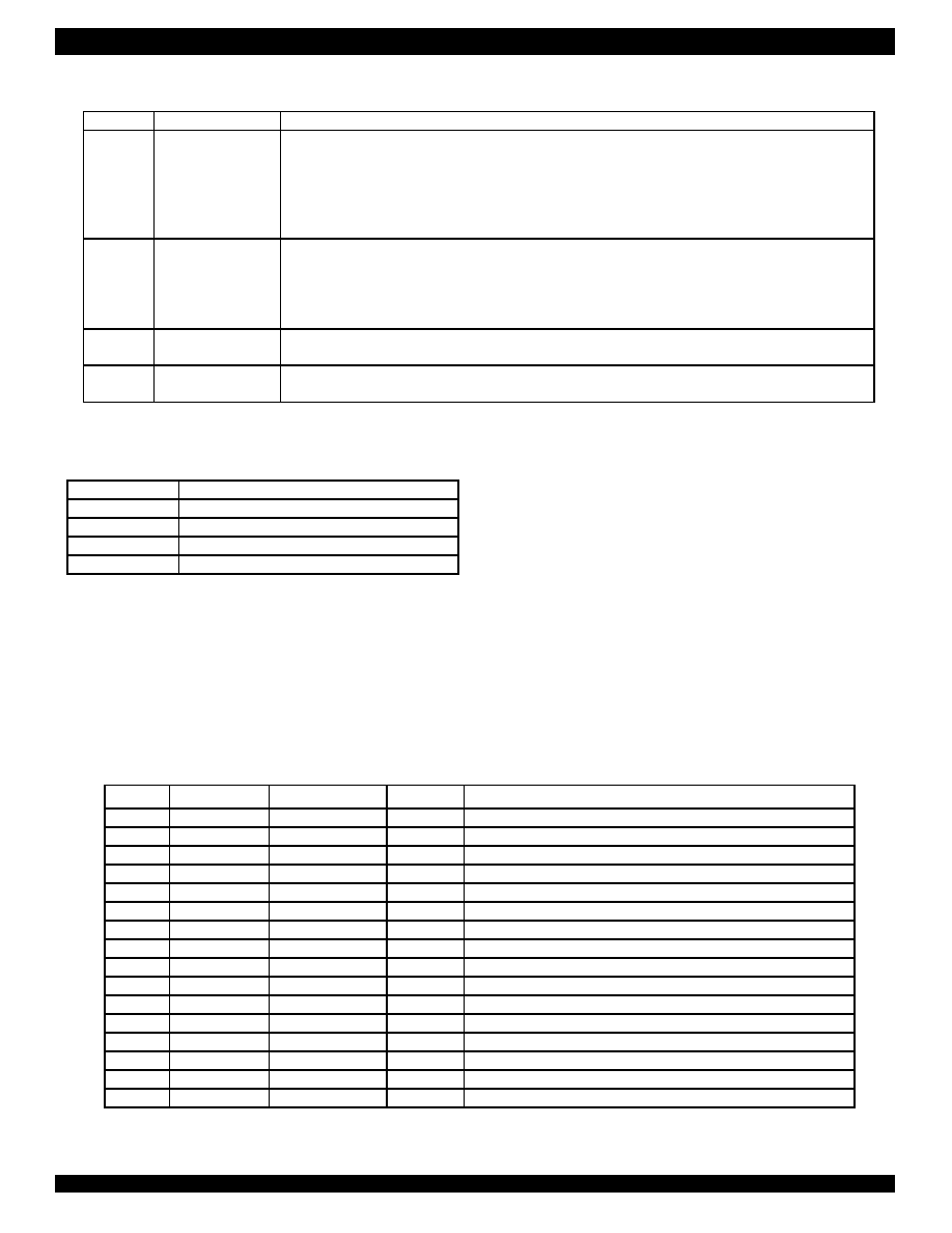
33
INDUSTRIAL TEMPERATURE RANGES
IDT82V2058 OCTAL E1 SHORT HAUL LINE INTERFACE UNIT
TABLE - 15. INSTRUCTION REGISTER DESCRIPTION
IR CODE
INSTRUCTION
COMMENTS
000
Extest
The external test instruction allows testing of the interconnection to other devices. When the current
instruction is the EXTEST instruction, the boundary scan register is placed between TDI and TDO.
The signal on the input pins can be sampled by loading the boundary scan register using the Capture-
DR state. The sampled values can then be viewed by shifting the boundary scan register using the
Shift-DR state. The signal on the output pins can be controlled by loading patterns shifted in through
input TDI into the boundary scan register using the Update-DR state.
100
Sample / Preload
The sample instruction samples all the device inputs and outputs. For this instruction, the boundary
scan register is placed between TDI and TDO. The normal path between the IDT82V2058 logic and
the I/O pins is maintained. Primary device inputs and outputs can be sampled by loading the boundary
scan register using the Capture-DR state. The sampled values can then be viewed by shifting the
boundary scan register using the Shift-DR state.
110
Idcode
The identification instruction is used to connect the identification register between TDI and TDO. The
device's identification code can then be shifted out using the Shift-DR state.
111
Bypass
The bypass instruction shifts data from input TDI to output TDO with one TCK clock period delay. The
instruction is used to bypass the device.
Bypass Register (BR)
The BR consists of a single bit. It can provide a serial path between
the TDI input and TDO output, bypassing the BSR to reduce test access
times.
Boundary Scan Register (BSR)
The BSR can apply and read test patterns in parallel to or from all
the digital I/O pins. The BSR is a 98 bits long shift register and is initialized
and read using the instruction EXTEST or SAMPLE/PRELOAD. Each
pin is related to one or more bits in the BSR. Please refer to Table-17
for details of BSR bits and their functions.
TEST ACCESS PORT CONTROLLER
The TAP controller is a 16-state synchronous state machine. Figure-
19 shows its state diagram. A description of each state follows. Note that
the figure contains two main branches to access either the data or
instruction registers. The value shown next to each state transition in
this figure states the value present at TMS at each rising edge of TCK.
Please refer to Table-18 for details of the state description.
BIT No. BIT SYMBOL
PIN SIGNAL
TYPE
COMMENTS
0
POUT0
LP0
I/O
1
PIN0
LP0
I/O
2
POUT1
LP1
I/O
3
PIN1
LP1
I/O
4
POUT2
LP2
I/O
5
PIN2
LP2
I/O
6
POUT3
LP3
I/O
7
PIN3
LP3
I/O
8
POUT4
LP4
I/O
9
PIN4
LP4
I/O
10
POUT5
LP5
I/O
11
PIN5
LP5
I/O
12
POUT6
LP6
I/O
13
PIN6
LP6
I/O
14
POUT7
LP7
I/O
15
PIN7
LP7
I/O
TABLE - 17. BOUNDARY SCAN REGISTER DESCRIPTION
BIT No.
COMMENTS
0
Set to "1"
1~11
Producer Number
12~27
Part Number
28~31
Device Revision
TABLE - 16. DEVICE IDENTIFICATION REGISTER DESCRIPTION

34
INDUSTRIAL TEMPERATURE RANGES
IDT82V2058 OCTAL E1 SHORT HAUL LINE INTERFACE UNIT
BIT No.
BIT SYMBOL
PIN SIGNAL
TYPE
COMMENTS
16
PIOS
N/A
-
Controls pin LP7~0.
When "0", the pins are configured as outputs. The output values to the
pins are set in POUT7~0.
When "1", the pins are tristated. The input values to the pins are read in
PIN7~0.
17
TCLK1
TCLK1
I
18
TDP1
TDP1
I
19
TDN1
TDN1
I
20
RCLK1
RCLK1
O
21
RDP1
RDP1
O
22
RDN1
RDN1
O
23
HZEN1
N/A
-
Controls pin RDP1, RDN1 and RCLK1.
When "0", the outputs are enabled on the pins.
When "1", the pins are tristated.
24
LOS1
LOS1
O
25
TCLK0
TCLK0
I
26
TDP0
TDP0
I
27
TDN0
TDN0
I
28
RCLK0
RCLK0
O
29
RDP0
RDP0
O
30
RDN0
RDN0
O
31
HZEN0
N/A
-
Controls pin RDP0, RDN0 and RCLK0.
When "0", the outputs are enabled on the pins.
When "1", the pins are tristated.
32
LOS0
LOS0
O
33
MODE1
MODE1
I
34
LOS3
LOS3
O
35
RDN3
RDN3
O
36
RDP3
RDP3
O
37
HZEN3
N/A
-
Controls pin RDP3, RDN3 and RCLK3.
When "0", the outputs are enabled on the pins.
When "1", the pins are tristated.
38
RCLK3
RCLK3
O
39
TDN3
TDN3
I
40
TDP3
TDP3
I
41
TCLK3
TCLK3
I
42
LOS2
LOS2
O
43
RDN2
RDN2
O
44
RDP2
RDP2
O
45
HZEN2
N/A
-
Controls pin RDP2, RDN2 and RCLK2.
When "0", the outputs are enabled on the pins.
When "1", the pins are tristated.
46
RCLK2
RCLK2
O
47
TDN2
TDN2
I
48
TDP2
TDP2
I
49
TCLK2
TCLK2
I
50
INT
INT
O
51
ACK
ACK
O
52
SDORDYS
N/A
-
Control pin ACK.
When "0", the output is enabled on pin ACK.
When "1", the pin is tristated.
53
WRB
DS
I
54
RDB
R/W
I
55
ALE
ALE
I
TABLE - 17. BOUNDARY SCAN REGISTER DESCRIPTION (CONTINUED)

35
INDUSTRIAL TEMPERATURE RANGES
IDT82V2058 OCTAL E1 SHORT HAUL LINE INTERFACE UNIT
BIT No.
BIT SYMBOL
PIN SIGNAL
TYPE
COMMENTS
56
CSB
CS
I
57
MODE0
MODE0
I
58
TCLK5
TCLK5
I
59
TDP5
TDP5
I
60
TDN5
TDN5
I
61
RCLK5
RCLK5
O
62
RDP5
RDP5
O
63
RDN5
RDN5
O
64
HZEN5
N/A
-
Controls pin RDP5, RDN5 and RCLK5.
When "0", the outputs are enabled on the pins.
When "1", the pins are tristated.
65
LOS5
LOS5
O
66
TCLK4
TCLK4
I
67
TDP4
TDP4
I
68
TDN4
TDN4
I
69
RCLK4
RCLK4
O
70
RDP4
RDP4
O
71
RDN4
RDN4
O
72
HZEN4
N/A
-
Controls pin RDP4, RDN4 and RCLK4.
When "0", the outputs are enabled on the pins.
When "1", the pins are tristated.
73
LOS4
LOS4
O
74
OE
OE
I
75
CLKE
CLKE
I
76
LOS7
LOS7
O
77
RDN7
RDN7
O
78
RDP7
RDP7
O
79
HZEN7
N/A
-
Controls pin RDP7, RDN7 and RCLK7.
When "0", the outputs are enabled on the pins.
When "1", the pins are tristated.
80
RCLK7
RCLK7
O
81
TDN7
TDN7
I
82
TDP7
TDP7
I
83
TCLK7
TCLK7
I
84
LOS6
LOS6
O
85
RDN6
RDN6
O
86
RDP6
RDP6
O
87
HZEN6
N/A
-
Controls pin RDP6, RDN6 and RCLK6.
When "0", the outputs are enabled on the pins.
When "1", the pins are tristated.
88
RCLK6
RCLK6
O
89
TDN6
TDN6
I
90
TDP6
TDP6
I
91
TCLK6
TCLK6
I
92
MCLK
MCLK
I
93
MODE2
MODE2
I
94
A4
A4
I
95
A3
A3
I
96
A2
A2
I
97
A1
A1
I
98
A0
A0
I
TABLE - 17. BOUNDARY SCAN REGISTER DESCRIPTION (CONTINUED)

36
INDUSTRIAL TEMPERATURE RANGES
IDT82V2058 OCTAL E1 SHORT HAUL LINE INTERFACE UNIT
STATE
DESCRIPTION
Test Logic
Reset
In this state, the test logic is disabled. The device is set to normal operation. During initialization, the device
initializes the instruction register with the IDCODE instruction.
Regardless of the original state of the controller, the controller enters the Test-Logic-Reset state when the TMS input
is held high for at least 5 rising edges of TCK. The controller remains in this state while TMS is high. The device
processor automatically enters this state at power-up.
Run-Test/Idle
This is a controller state between scan operations. Once in this state, the controller remains in the state as long as
TMS is held low. The instruction register and all test data registers retain their previous state. When TMS is high and a
rising edge is applied to TCK, the controller moves to the Select-DR state.
Select-DR-Scan
This is a temporary controller state and the instruction does not change in this state. The test data register selected
by the current instruction retains its previous state. If TMS is held low and a rising edge is applied to TCK when in this
state, the controller moves into the Capture-DR state and a scan sequence for the selected test data register is initiated.
If TMS is held high and a rising edge applied to TCK, the controller moves to the Select-IR-Scan state.
Capture-DR
In this state, the Boundary Scan Register captures input pin data if the current instruction is EXTEST or
SAMPLE/PRELOAD. The instruction does not change in this state. The other test data registers, which do not have
parallel input, are not changed. When the TAP controller is in this state and a rising edge is applied to TCK, the
controller enters the Exit1-DR state if TMS is high or the Shift-DR state if TMS is low.
Shift-DR
In this controller state, the test data register connected between TDI and TDO as a result of the current instruction
shifts data on stage toward its serial output on each rising edge of TCK. The instruction does not change in this state.
When the TAP controller is in this state and a rising edge is applied to TCK, the controller enters the Exit1-DR state if
TMS is high or remains in the Shift-DR state if TMS is low.
Exit1-DR
This is a temporary state. While in this state, if TMS is held high, a rising edge applied to TCK causes the controller
to enter the Update-DR state, which terminates the scanning process. If TMS is held low and a rising edge is applied to
TCK, the controller enters the Pause-DR state. The test data register selected by the current instruction retains its
previous value and the instruction does not change during this state.
Pause-DR
The pause state allows the test controller to temporarily halt the shifting of data through the test data register in the
serial path between TDI and TDO. For example, this state could be used to allow the tester to reload its pin memory
from disk during application of a long test sequence. The test data register selected by the current instruction retains its
previous value and the instruction does not change during this state. The controller remains in this state as long as TMS
is low. When TMS goes high and a rising edge is applied to TCK, the controller moves to the Exit2-DR state.
Exit2-DR
This is a temporary state. While in this state, if TMS is held high, a rising edge applied to TCK causes the controller
to enter the Update-DR state, which terminates the scanning process. If TMS is held low and a rising edge is applied to
TCK, the controller enters the Shift-DR state. The test data register selected by the current instruction retains its
previous value and the instruction does not change during this state.
Update-DR
The Boundary Scan Register is provided with a latched parallel output to prevent changes while data is shifted in
response to the EXTEST and SAMPLE/PRELOAD instructions. When the TAP controller is in this state and the
Boundary Scan Register is selected, data is latched into the parallel output of this register from the shift-register path on
the falling edge of TCK. The data held at the latched parallel output changes only in this state. All shift-register stages in
the test data register selected by the current instruction retain their previous value and the instruction does not change
during this state.
Select-IR-Scan
This is a temporary controller state. The test data register selected by the current instruction retains its previous
state. If TMS is held low and a rising edge is applied to TCK when in this state, the controller moves into the Capture-IR
state, and a scan sequence for the instruction register is initiated. If TMS is held high and a rising edge is applied to
TCK, the controller moves to the Test-Logic-Reset state. The instruction does not change during this state.
Capture-IR
In this controller state, the shift register contained in the instruction register loads a fixed value of `100' on the rising
edge of TCK. This supports fault-isolation of the board-level serial test data path. Data registers selected by the current
instruction retain their value and the instruction does not change during this state. When the controller is in this state
and a rising edge is applied to TCK, the controller enters the Exit1-IR state if TMS is held high, or the Shift-IR state if
TMS is held low.
Shift-IR
In this state, the shift register contained in the instruction register is connected between TDI and TDO and shifts data
one stage towards its serial output on each rising edge of TCK. The test data register selected by the current instruction
retains its previous value and the instruction does not change during this state. When the controller is in this state and a
rising edge is applied to TCK, the controller enters the Exit1-IR state if TMS is held high, or remains in the Shift-IR state
if TMS is held low.
TABLE - 18. TAP CONTROLLER STATE DESCRIPTION
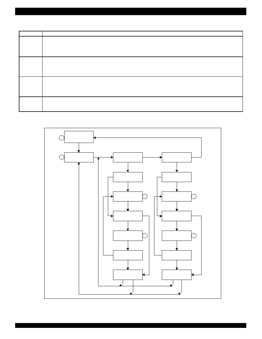
37
INDUSTRIAL TEMPERATURE RANGES
IDT82V2058 OCTAL E1 SHORT HAUL LINE INTERFACE UNIT
STATE
DESCRIPTION
Exit1-IR
This is a temporary state. While in this state, if TMS is held high, a rising edge applied to TCK causes the controller to
enter the Update-IR state, which terminates the scanning process. If TMS is held low and a rising edge is applied to TCK, the
controller enters the Pause-IR state. The test data register selected by the current instruction retains its previous value and
the instruction does not change during this state.
Pause-IR
The pause state allows the test controller to temporarily halt the shifting of data through the instruction register. The test
data register selected by the current instruction retains its previous value and the instruction does not change during this
state. The controller remains in this state as long as TMS is low. When TMS goes high and a rising edge is applied to TCK,
the controller moves to the Exit2-IR state.
Exit2-IR
This is a temporary state. While in this state, if TMS is held high, a rising edge applied to TCK causes the controller to
enter the Update-IR state, which terminates the scanning process. If TMS is held low and a rising edge is applied to TCK, the
controller enters the Shift-IR state. The test data register selected by the current instruction retains its previous value and the
instruction does not change during this state.
Update-IR
The instruction shifted into the instruction register is latched into the parallel output from the shift-register path on the falling
edge of TCK. When the new instruction has been latched, it becomes the current instruction. The test data registers selected
by the current instruction retain their previous value.
TABLE - 19. TAP CONTROLLER STATE DESCRIPTION (CONTINUED)
Test-logic Reset
Run Test/Idle
Select-DR
Select-IR
Capture-DR
Capture-IR
Shift-DR
Shift-IR
Exit1-DR
Exit1-IR
Pause-DR
Pause-IR
Exit2-DR
Exit2-IR
Update-DR
Update-IR
1
0
0
1
1
1
0
0
0
0
0
0
1
1
1
0
1
0
1
1
1
0
1
0
1
0
1
1
0
0
0
1
Figure - 19. JTAG State Diagram

38
INDUSTRIAL TEMPERATURE RANGES
IDT82V2058 OCTAL E1 SHORT HAUL LINE INTERFACE UNIT
ABSOLUTE MAXIMUM RATING
RECOMMENDED OPERATING CONDITIONS
Symbol
Parameter
Min
Typ
Max
Unit
VDDA,VDDD
Core Power Supply
3.13
3.3
3.47
V
VDDIO
I/O Power Supply
3.13
3.3
3.47
V
3.13
3.3
3.47
V
VDDT
Transmitter Supply
3.3V
5V
4.75
5.0
5.25
V
T
A
Ambient operating temperature
-40
25
85
∞
C
R
L
Output load at TTIP and TRING
25
I
VDD
Average core power supply current
(1)
40
60
mA
I
VDDIO
IO power supply current
(3)
15
25
mA
I
VDDT
Average transmitter power supply current, E1
mode
(1, 2)
75
50% ones density data:
100% ones density data:
120
50% ones density data:
100% ones density data:
125
220
100
200
mA
Symbol
Parameter
Min
Max
Unit
VDDA,VDDD
Core Power Supply
-0.5
4.0
V
VDDIO0,VDDIO1
I/O Power Supply
-0.5
4.0
V
VDDT0-7
Transmit Power Supply
-0.5
7.0
V
Input Voltage, Any Digital Pin
GND-0.5
5.5
V
Input Voltage, Any RTIP and RRING pin
(1)
GND-0.5
VDDA+0.5
VDDD+0.5
V
Vin
ESD Voltage, any pin
(2)
2000
V
Transient latch-up current, any pin
100
mA
Input current, any digital pin
(3)
-10
10
mA
Iin
DC Input current, any analog pin
(3)
±
100
mA
Pd
Maximum power dissipation in package
1.6
W
Tc
Case Temperature
120
∞
C
Ts
Storage Temperature
-65
+150
∞
C
CAUTION
Exceeding these values may cause permanent damage. Functional operation under these conditions is not implied.
Exposure to absolute maximum rating conditions for extended periods may affect device reliability.
NOTE:
1. Referenced to ground
2. Human body model
3. Constant input current
NOTE:
1. Maximum power and current consumption over the full operating temperature and power supply voltage range. Includes all channels.
2. Power consumption includes power absorbed by line load and external transmitter components.
3. Digital output is driving 50pF load, digital input is within 10% of the supply rails.
39
INDUSTRIAL TEMPERATURE RANGES
IDT82V2058 OCTAL E1 SHORT HAUL LINE INTERFACE UNIT
POWER CONSUMPTION
Symbol
Parameter
LEN
Min
Typ
Max
(1, 2)
Unit
E1, 3.3V, 75
Load
50% ones density data:
100% ones density data:
000
000
-
-
612
1050
-
1125
mW
E1, 3.3V, 120
Load
50% ones density data:
100% ones density data:
000
000
-
-
526
880
-
940
mW
E1, 5.0V, 75
Load
50% ones density data:
100% ones density data:
000
000
-
-
835
1510
-
1610
mW
E1, 5.0V, 120
Load
50% ones density data:
100% ones density data:
000
000
-
-
710
1240
-
1330
mW
NOTE:
1. Maximum power and current consumption over the full operating temperature and power supply voltage range. Includes all channels.
2. Power consumption includes power absorbed by line load and external transmitter components.
3. T1 maximum values measured with maximum cable length (LEN = 111). Typical values measured with typical cable length (LEN = 101).
DC CHARACTERISTICS
Symbol
Parameter
Min
Typ
Max
Unit
Input Low Level Voltage
MODE2, JAS, LPn pins
1
3 VDDIO-0.2
V
IL
All other digital inputs pins
0.8
V
Input Mid Level Voltage
V
IM
MODE2, JAS, LPn pins
1
3 VDDIO+0.2
1
2 VDDIO
2
3 VDDIO-0.2
V
Input High Voltage
MODE2, JAS, LPn pins
2
3 VDDIO+ 0.2
V
IH
All other digital inputs pins
2.0
V
V
OL
Output Low level Voltage
(1)
(Iout=1.6mA)
0.4
V
V
OH
Output High level Voltage
(1)
(Iout=400
µ
A)
2.4
VDDIO
V
V
MA
Analog Input Quiescent Voltage
(RTIP, RRING pin while floating)
1.33
1.4
1.47
V
I
H
Input High Level Current
(MODE2, JAS, LPn pin)
50
µ
A
I
L
Input Low Level Current
(MODE2, JAS, LPn pin)
50
µ
A
I
I
Input Leakage Current
TMS, TDI, TRST
All other digital input pins
-10
50
10
µ
A
µA
I
ZL
Tri-state Leakage Current
-10
10
µ
A
Z
OH
Output High Impedance on (TTIP, TRING Pins)
150
K
NOTE:
1. Output drivers will output CMOS logic levels into CMOS loads.
40
INDUSTRIAL TEMPERATURE RANGES
IDT82V2058 OCTAL E1 SHORT HAUL LINE INTERFACE UNIT
TRANSMITTER CHARACTERISTICS
Symbol
Parameter
Min
Typ
Max
Unit
V
0-p
Output pulse amplitudes
(1)
E1, 75
load
E1,120
load
2.14
2.7
2.37
3.0
2.6
3.3
V
V
V
O-S
Zero (space) level
E1, 75
load
E1,120
load
-0.237
-0.3
0.237
0.3
V
V
Transmit amplitude variation with supply
-1
+1
%
Difference between pulse sequences for 17 consecutive pulses
200
mV
T
PW
Output Pulse Width at 50% of nominal amplitude:
232
244
256
ns
Ratio of the amplitudes of Positive and Negative Pulses at the
center of the pulse interval
0.95
1.05
Transmit Return Loss
(2)
E1,75
51 KHz ≠ 102 KHz
102 KHz - 2.048 MHz
2.048 MHz ≠ 3.072 MHz
15
15
15
dB
dB
dB
RTX
E1,120
51 KHz ≠ 102 KHz
102 KHz - 2.048 MHz
2.048 MHz ≠ 3.072 MHz
15
15
15
dB
dB
dB
Intrinsic Transmit Jitter (TCLK is jitter free, JA enable)
JTX
P-P
E1: 20 HZ ≠ 100 KHz
0.050
U.I.
Transmit path delay (JA is disabled)
Td
Single rail
Dual rail
8
3
U.I.
U.I.
I
SC
Line short circuit current
(3)
150
mA
Ip-p
NOTE:
1. E1:measured at the line output ports
2. Test at IDT82V2058 evaluation board
3. Measured at 2x9.5
series resistors and 1:2 transformer

41
INDUSTRIAL TEMPERATURE RANGES
IDT82V2058 OCTAL E1 SHORT HAUL LINE INTERFACE UNIT
JITTER ATTENUATOR CHARACTERISTICS
Symbol
Parameter
Min
Typ
Max
Unit
Jitter Transfer Function Corner (≠3dB) Frequency
Host mode: 32/64 bit FIFO
JABW = 0:
JABW = 1:
1.7
6.6
Hz
Hz
f
-3dB
Hardware mode
1.7
Hz
Jitter Attenuator
(1)
@ 3 Hz
@ 40 Hz
@ 400 Hz
@ 100kHz
-0.5
-0.5
+19.5
+19.5
dB
Jitter Attenuator Latency Delay
td
32bit FIFO:
64bit FIFO:
16
32
U.I.
U.I.
Input jitter tolerance before FIFO overflow or underflow
32bit FIFO:
64bit FIFO:
28
56
U.I.
U.I.
Output jitter in remote loopback
(2)
0.11
U.I.
NOTE:
1. Per G.736, see Fig-35.
2. Per ETSI CTR12/13 Output jitter.
RECEIVER CHARACTERISTICS
Symbol
Parameter
Min
Typ
Max
Unit
ATT
Permissible Cable Attenuation (@1024kHz)
15
dB
IA
Input Amplitude
0.1
0.8
Vp
SIR
Signal to Interference Ratio Margin
(1)
-14
dB
SRE
Data decision threshold (reference to peak input voltage)
50
%
Data slicer threshold
150
mV
Analog loss of signal
(2)
Threshold:
Hysteresis:
310
230
mV
mV
Allowable consecutive zeros before LOS
E1, G.775:
E1, ETSI300233:
32
2048
LOS reset
Clock recovery mode
12.5
% ones
JRX
p-p
Peak to Peak Intrinsic Receive Jitter (JA disabled)
0.0625
U.I.
Jitter Tolerance
JTRX
1 Hz ≠ 20 Hz
20 Hz ≠ 2.4 KHz
18 KHz ≠ 100 KHz
18.0
1.5
0.2
U.I.
U.I.
U.I.
ZDM
Receiver Differential Input Impedance
120
K
ZCM
Receiver Common Mode Input Impedance to GND
10
K
RRX
Receive Return Loss
51 KHz ≠ 102 KHz
102 KHz - 2.048 MHz
2.048 MHz ≠ 3.072 MHz
20
20
20
db
dB
dB
Receive path delay
Dual rail
Single rail
3
8
U.I.
U.I.
NOTE:
1. E1: per G.703, O.151 @6dB cable attenuation.
2. The test circuit for this parameter is shown in Figure 12. The analog signal is measured on the Receiver line before the transformer (port A and port B in Figure 12). And
the receive line is a T1/E1 cable simulator.
42
INDUSTRIAL TEMPERATURE RANGES
IDT82V2058 OCTAL E1 SHORT HAUL LINE INTERFACE UNIT
TRANSCEIVER TIMING CHARACTERISTICS
Symbol
Parameter
Min
Typ
Max
Unit
MCLK frequency
2.048
MHz
MCLK tolerance
-100
100
ppm
MCLK duty cycle
40
60
%
Transmit path
TCLK frequency
2.048
MHz
TCLK tolerance
-50
+50
ppm
TCLK Duty Cycle
10
90
%
t1
Transmit Data Setup Time
40
ns
t2
Transmit Data Hold Time
40
ns
Delay time of OE low to driver High Z
1
us
Delay time of TCLK low to driver High Z
40
44
48
us
Receive path
Clock recovery capture range
(1)
+/- 80
ppm
RCLK duty cycle
(2)
40
50
60
%
t4
RCLK pulse width
(2)
457
488
519
ns
t5
RCLK pulse width low time
203
244
285
ns
t6
RCLK pulse width high time
203
244
285
ns
Rise/fall time
(3)
20
ns
t7
Receive Data Setup Time
200
244
ns
t8
Receive Data Hold Time
200
244
ns
t9
RDN/RDP pulse width (MCLK = H)
(4)
200
244
ns
NOTE:
1. Relative to nominal frequency, MCLK=+/-100 ppm
2. RCLK duty cycle widths will vary depending on extent of received pulse jitter displacement. Maximum and minimum RCLK duty cycles are for worst case jitter conditions (0.2UI displacement
for E1 per ITU G.823).
3. For all digital outputs. C load = 15 pF
4. Clock recovery is disabled in this mode.
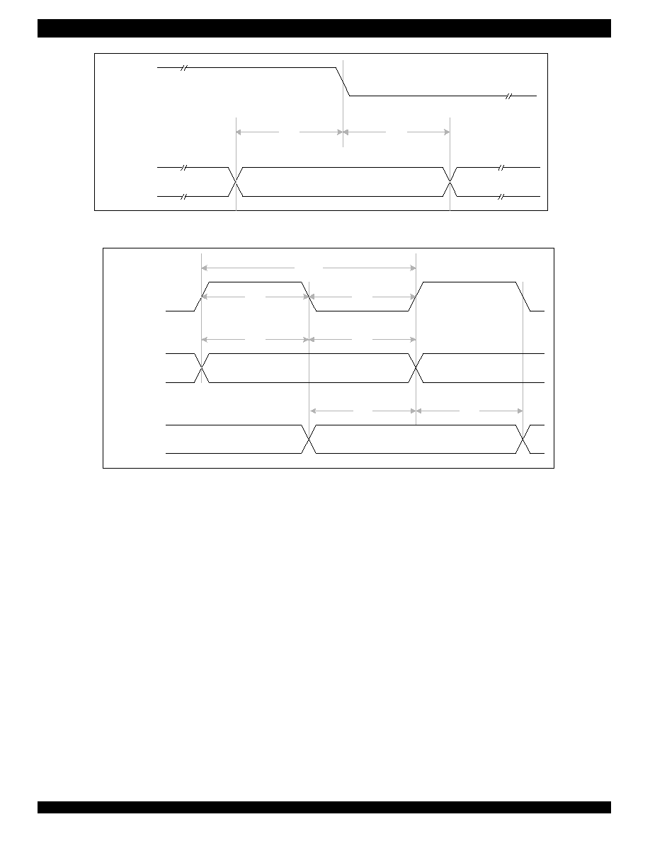
43
INDUSTRIAL TEMPERATURE RANGES
IDT82V2058 OCTAL E1 SHORT HAUL LINE INTERFACE UNIT
Figure - 21. Transmit System Interface Timing
Figure - 22. Receive System Interface Timing
TDNn/BPVIn
TNn/TDPn
TCLK
t1
t2
RDNn/CVn
RDPn/RDn
RCLK
t4
t7
t6
t7
t5
t8
t8
(CLKE = 0)
(CLKE = 1)
RDPn/RDn
RDNn/CVn
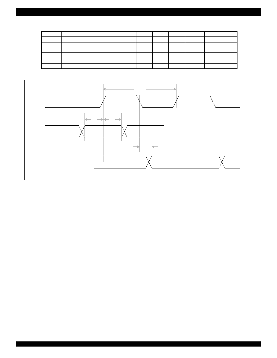
44
INDUSTRIAL TEMPERATURE RANGES
IDT82V2058 OCTAL E1 SHORT HAUL LINE INTERFACE UNIT
JTAG TIMING CHARACTERISTICS
Symbol
Parameter
Min
Typ
Max
Unit
Comments
t1
TCK Period
200
ns
t2
TMS to TCK setup Time
TDI to TCK Setup Time
50
ns
t3
TCK to TMS Hold Time
TCK to TDI Hold Time
50
ns
t4
TCK to TDO Delay Time
100
ns
Figure - 23. JTAG Interface Timing
TCK
t1
t2
t3
TDO
TMS
TDI
t4

45
INDUSTRIAL TEMPERATURE RANGES
IDT82V2058 OCTAL E1 SHORT HAUL LINE INTERFACE UNIT
PARALLEL HOST INTERFACE TIMING CHARACTERISTICS
INTEL MODE READ TIMING CHARACTERISTICS
Symbol
Parameter
Min Typ Max Unit Comments
t1
Active RD Pulse Width
90
ns
note 1
t2
Active CS to Active RD Setup Time
0
ns
t3
Inactive RD to Inactive CS Hold Time
0
ns
t4
Valid Address to Inactive ALE Setup Time (in Multiplexed Mode)
5
ns
t5
Invalid RD to Address Hold Time (in Non-Multiplexed Mode)
0
ns
t6
Active RD to Data Output Enable Time
7.5
15 ns
t7
Inactive RD to Data Tri-State Delay Time
7.5
15 ns
t8
Active CS to RDY delay time
6
12 ns
t9
Inactive CS to RDY Tri-state Delay Time
6
12 ns
t10
Inactive RD to Inactive INT Delay Time
20 ns
t11
Address Latch Enable Pulse Width (in Multiplexed Mode)
10
ns
t12
Address Latch Enable to RD Setup Time (in Multiplexed Mode)
0
ns
t13
Address Setup time to Valid Data Time (in Non-Multiplexed Mode)
Inactive ALE to Valid Data Time (in Multiplexed Mode)
18
32 ns
t14
Inactive RD to Active RDY Delay Time
10
15 ns
t15
Active RD to Active RDY Delay Time
30
85 ns
t16
Inactive ALE to Address Hold Time (in Multiplexed Mode)
5
ns
Note 1: the t1 is determined by the start time of the valid data when the RDY signal is not used.

46
INDUSTRIAL TEMPERATURE RANGES
IDT82V2058 OCTAL E1 SHORT HAUL LINE INTERFACE UNIT
Figure - 25. Multiplexed Intel Mode Read Timing
Figure - 24. Non-Multiplexed Intel Mode Read Timing
INT
RDY
D[7:0]
A[7:0]
ALE(=1)
RD
CS
t1
t2
t3
t5
t6
t7
t8
t9
t10
t13
ADDRESS
DATA OUT
t14
t15
INT
RDY
AD[7:0]
ALE
RD
CS
t1
t2
t3
t6
t7
t8
t9
t10
t4
t11
t12
ADDRESS
DATA OUT
t15
t14
t16
t13

47
INDUSTRIAL TEMPERATURE RANGES
IDT82V2058 OCTAL E1 SHORT HAUL LINE INTERFACE UNIT
Symbol
Parameter
Min Typ Max Unit Comments
t1
Active WR Pulse Width
90
ns
note 1
t2
Active CS to Active WR Setup Time
0
ns
t3
Inactive WR to Inactive CS Hold Time
0
ns
t4
Valid Address to Latch Enable Setup Time (in Multiplexed Mode)
5
ns
t5
Invalid WR to Address Hold Time (in Non-Multiplexed Mode)
2
ns
t6
Valid Data to Inactive WR Setup Time
5
ns
t7
Inactive WR to Data Hold Time
10
ns
t8
Active CS to Inactive RDY Delay Time
6
12
ns
t9
Active WR to Active RDY Delay Time
30
85
ns
t10
Inactive WR to Inactive RDY Delay Time
10
15
ns
t11
Invalid CS to RDY Tri-State Delay Time
6
12
ns
t12
Address Latch Enable Pulse Width (in Multiplexed Mode)
10
ns
t13
Inactive ALE to WR Setup Time (in Multiplexed Mode)
0
ns
t14
Inactive ALE to Address hold time (in Multiplexed Mode)
5
ns
t15
Address setup time to Inactive WR time (in Non-Multiplexed Mode)
5
ns
Note 1: the t1 can be 15ns when RDY signal is not used.
INTEL MODE WRITE TIMING CHARACTERISTICS
Figure - 27. Multiplexed Intel Mode Write Timing
Figure - 26. Non-Multiplexed Intel Mode Write Timing
RDY
D[7:0]
A[7:0]
ALE(=1)
WR
CS
t2
t1
t3
t5
t6
t7
t8
t9
t10
t11
ADDRESS
WRITE DATA
t15
RDY
AD[7:0]
ALE
WR
CS
t1
t2
t3
t6
t7
t8
t9
t10
t4
t12
t13
WRITE DATA
ADDRESS
t11
t14
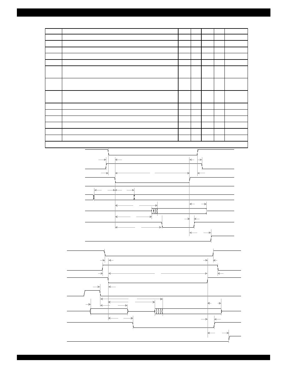
48
INDUSTRIAL TEMPERATURE RANGES
IDT82V2058 OCTAL E1 SHORT HAUL LINE INTERFACE UNIT
Figure - 28. Non-Multiplexed Motorola Mode Read Timing
Figure - 29. Multiplexed Motorola Mode Read Timing
INT
ACK
D[7:0]
A[7:0]
ALE(=1)
DS
CS
t1
ADDRESS
DATA OUT
R/W
t2
t3
t4
t5
t6
t8
t10
t11
t12
t13
t7
t9
INT
ACK
AD[7:0]
AS
DS
CS
DATA OUT
ADDRESS
R/W
t1
t2
t3
t4
t5
t6
t7
t8
t11
t10
t12
t13
t14
t9
Symbol
Parameter
Min Typ Max Unit Comments
t1
Active DS Pulse Width
90
ns
note 1
t2
Active CS to Active DS Setup Time
0
ns
t3
Inactive DS to Inactive CS Hold Time
0
ns
t4
Valid R/W to Active DS Setup Time
0
ns
t5
Inactive DS to R/W Hold Time
0.5
ns
t6
Valid Address to Active DS Setup Time (in Non-Multiplexed Mode)
Valid Address to AS Setup Time (in Multiplexed Mode)
5
ns
t7
Active DS to Address Hold Time (in Non-Multiplexed Mode)
Active AS to Address Hold Time (in Multiplexed Mode)
10
ns
t8
Active DS to Data Valid Delay Time (in Non-Multiplexed Mode)
Active AS to Data Valid Delay Time ( in Multiplexed Mode)
20
35
ns
t9
Active DS to Data Output Enable Time
7.5
15
ns
t10
Inactive DS to Data Tri-State Delay Time
7.5
15
ns
t11
Active DS to Active ACK Delay Time
30
85
ns
t12
Inactive DS to Inactive ACK Delay Time
10
15
ns
t13
Inactive DS to Invalid INT Delay Time
20
ns
t14
Active AS to Active DS Setup Time (in Multiplexed Mode)
5
ns
Note 1: the t1 is determined by the start time of the valid data when the ACK signal is not used.
MOTOROLA MODE READ TIMING CHARACTERISTICS

49
INDUSTRIAL TEMPERATURE RANGES
IDT82V2058 OCTAL E1 SHORT HAUL LINE INTERFACE UNIT
Symbol
Parameter
Min Typ Max Unit Comments
t1
Active DS Pulse Width
90
ns
note 1
t2
Active CS to Active DS Setup Time
0
ns
t3
Inactive DS to Inactive CS Hold Time
0
ns
t4
Valid R/W to Active DS Setup Time
10
ns
t5
Inactive DS to R/W Hold Time
0
ns
t6
Valid Address to Active DS Setup Time (in Non-Multiplexed Mode)
Valid Address to AS Setup Time (in Multiplexed Mode)
10
ns
t7
Valid DS to Address Hold Time (in Non-Multiplexed Mode)
Valid AS to Address Hold Time (in Multiplexed Mode)
10
ns
t8
Valid Data to Inactive DS Setup Time
5
ns
t9
Inactive DS to Data Hold Time
10
ns
t10
Active DS to Active ACK Delay Time
30
85
ns
t11
Inactive DS to Inactive ACK Delay Time
10
15
ns
t12
Active AS to Active DS (in Multiplexed Mode)
0
ns
t13
Inactive DS to Inactive AS Hold Time ( in Multiplexed Mode)
15
ns
Note 1: the t1 can be 15ns when the ACK signal is not used.
Figure - 30. Non-Multiplexed Motorola Mode Write Timing
ACK
D[7:0]
A[7:0]
ALE(=1)
DS
CS
t1
ADDRESS
WRITE DATA
R/W
t2
t3
t4
t6
t7
t5
t8
t9
t10
t11
MOTOROLA MODE WRITE TIMING CHARACTERISTICS
Figure - 31. Multiplexed Motorola Mode Writing Timing
ACK
AD[7:0]
AS
DS
CS
WRITE DATA
ADDRESS
R/W
t1
t2
t3
t4
t5
t6
t7
t8
t9
t13
t10
t11
t12

50
INDUSTRIAL TEMPERATURE RANGES
IDT82V2058 OCTAL E1 SHORT HAUL LINE INTERFACE UNIT
Figure - 34. Serial Interface Read Timing with CLKE = 1
Figure - 33. Serial Interface Read Timing with CLKE = 0
Figure - 32. Serial Interface Write Timing
MSB
LSB
LSB
CS
SCLK
SDI
t1
t2
t3
t4
t5
t6
t7
t7
CONTROL BYTE
DATA BYTE
1
2
3
4
5
6
7
8
9
10
11
12
13
14
15
16
7
6
5
4
3
2
1
0
SDO
CS
SCLK
t4
t11
1
2
3
4
5
6
7
8
9
10
11
12
13
14
15
16
7
6
5
4
3
2
1
0
SDO
CS
SCLK
t4
t11
Symbol
Parameter
Min
Typ
Max
Unit Comments
t1
SCLK High Time
25
ns
t2
SCLK Low Time
25
ns
t3
Active CS to SCLK Setup Time
10
ns
t4
Last SCLK Hold Time to Inactive CS Time
50
ns
t5
CS Idle Time
50
ns
t6
SDI to SCLK Setup Time
5
ns
t7
SCLK to SDI Hold Time
5
ns
t8
Rise/Fall Time (any pin)
100
ns
t9
SCLK Rise and Fall Time
50
ns
t10
SCLK to SDO Valid Delay Time
100
ns
t11
SCLK Falling Edge to SDO tri-state Hold Time (CLKE = 0)
CS Rising Edge to SDO tri-state Hold Time (CLKE = 1)
100
ns
SERIAL HOST INTERFACE TIMING CHARACTERISTICS
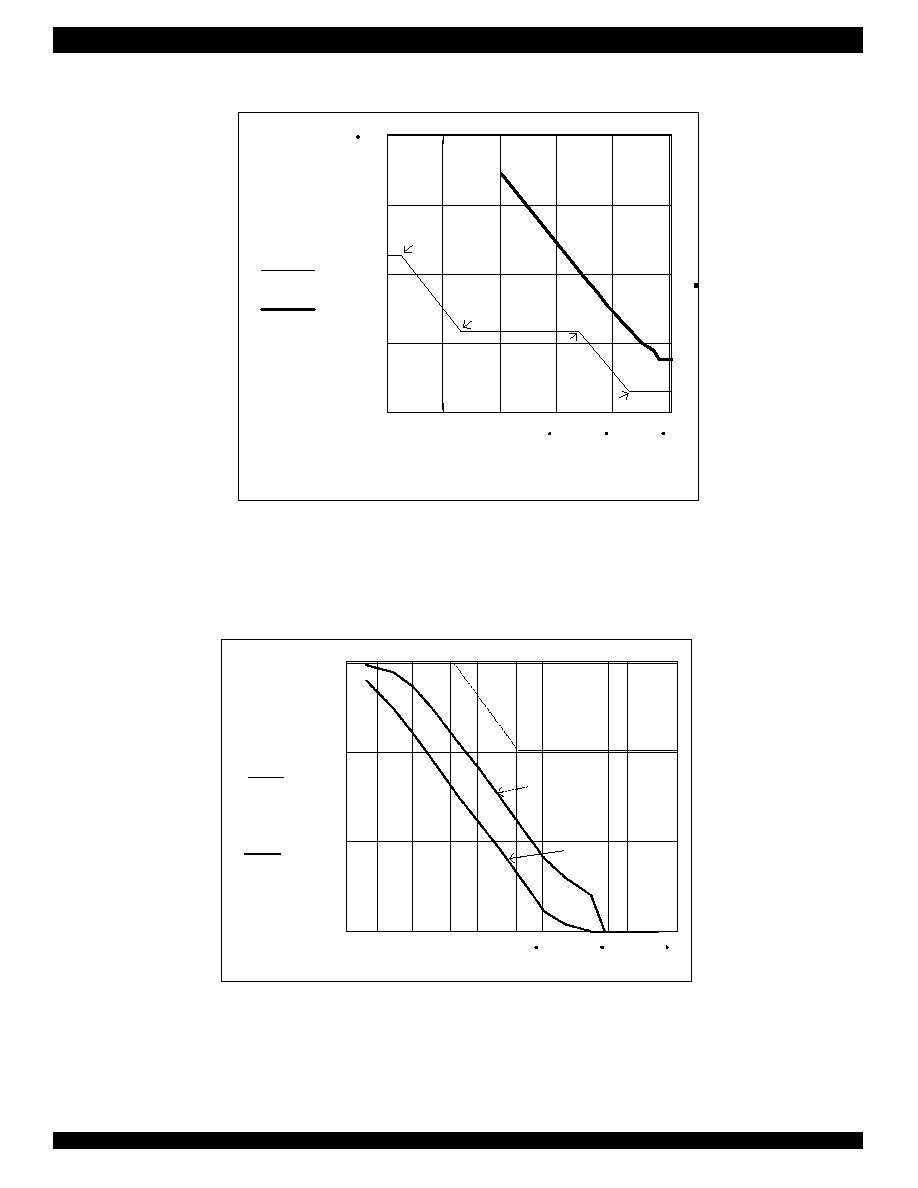
51
INDUSTRIAL TEMPERATURE RANGES
IDT82V2058 OCTAL E1 SHORT HAUL LINE INTERFACE UNIT
JITTER TOLERANCE PERFORMANCE
G.823
IDT82V2048
1
10
100
1 103
1 104
1 105
0.1
1
10
100
1 103
18 UI @ 1.8 Hz
1.5 UI @ 20 Hz
1.5 UI @ 2.4
kHz
0.2 UI @ 18 kHz
Frequency (Hz)
Jitter (UI)
Test condition: PRBS 2^15-1; Line code rule HDB3 is used.
Figure - 35. E1 Jitter Tolerance Performance
JITTER TRANSFER PERFORMANCE
Test condition: PRBS 2^15-1; Line code rule HDB3 is used.
Figure - 36. E1 Jitter Transfer Performance
G.736
1
10
100
1 103
1 104
1 105
-60
-40
-20
0
IDT82V2048
0.5 dB @ 3 Hz 0.5 dB @ 40 Hz
-19.5 dB @
400 Hz
-19.5 dB @ 20 kHz
f
3dB
= 6.5 Hz
f
3dB
= 1.7 Hz
Frequency (Hz)
Gain (dB)
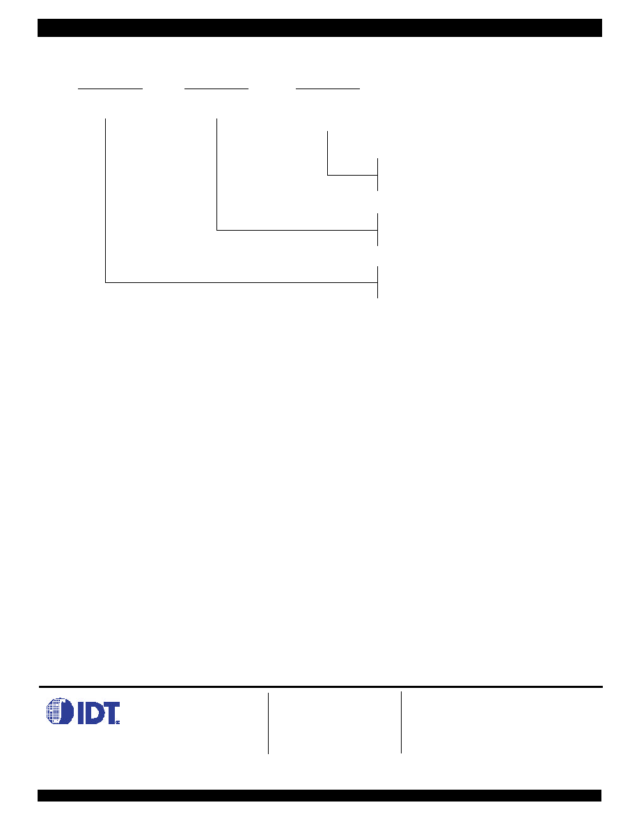
52
INDUSTRIAL TEMPERATURE RANGES
IDT82V2058 OCTAL E1 SHORT HAUL LINE INTERFACE UNIT
CORPORATE HEADQUARTERS for SALES:
for Tech Support:
2975 Stender Way
800-345-7015 or 408-727-6116
408-330-1753
Santa Clara, CA 95054
fax: 408-492-8674
email: telecomhelp@idt.com
*To search for sales office near you, please click the sales button found on our home page or dial the 800# above and press 2.
The IDT logo is a registered trademark of Integrated Device Technology, Inc.
www.idt.com*
Data Sheet Document History
11/4/2001
pgs. 2, 3, 10, 17
11/20/2001
pgs. 5, 6, 11, 13, 16, 17, 24, 26, 31, 38, 39, 40, 50
11/28/2001
pgs. 5, 24, 26, 31
11/29/2001
pgs. 5
12/5/2001 pgs. 9
1/24/2002 pgs. 2, 3, 9, 14, 39, 40
2/21/2002 pgs. 14, 16, 41
3/25/2002
pgs. 1, 2, 52
4/17/2002 pgs. 17
5/7/2002 pgs. 14, 44, 45, 48
1/15/2003 pgs. 1, 52
IDT
XXXXXXX
XX
X
Device Type
Blank
Process/
Temperature
Range
BB
82V2058
Industrial (-40 ∞C to +85 ∞C)
Plastic Ball Grid Array (PBGA, BB160)
E1 Short Haul LIU
DA
Thin Quad Flatpack (TQFP, DA144)
ORDERING INFORMATION