 | –≠–ª–µ–∫—Ç—Ä–æ–Ω–Ω—ã–π –∫–æ–º–ø–æ–Ω–µ–Ω—Ç: 82V3002A | –°–∫–∞—á–∞—Ç—å:  PDF PDF  ZIP ZIP |

1
The IDT logo is a registered trademark of Integrated Device Technology, Inc.
INDUSTRIAL TEMPERATURE RANGE
2003 Integrated Device Technology, Inc.
MAY, 2003
DSC-6243/-
WAN PLL WITH DUAL
REFERENCE INPUTS
ADVANCE INFORMATION
IDT82V3002A
DESCRIPTION
The IDT82V3002A is a WAN PLL with dual reference inputs. It
contains a Digital Phase-Locked Loop (DPLL), which generates ST-BUS
clocks and framing signals that are phase locked to a 2.048 MHz, 1.544
MHz or 8 kHz input reference.
The IDT82V3002A provides eight types of clock signals (C1.5o, C3o,
C6o, C2o, C4o, C8o, C16o, C32o) and six types of framing signals (F0o,
F8o, F16o, F32o, RSP, TSP) for the multitrunk T1 and E1 primary rate
transmission links.
The IDT82V3002A is compliant with AT&T TR62411, Telcordia GR-
1244-CORE Stratum 3, Stratum 4 Enhanced and Stratum 4, ETSI ETS
300 011, ITU-T G.813 Option 1 for 2048 kbit/s interface, and ITU-T G.812
FEATURES
∑ Supports AT&T TR62411 and Telcordia GR-1244-CORE Stra-
tum
3, Stratum 4 Enhanced and Stratum 4 timing for DS1
interfaces
∑ Supports ITU-T G.813 Option 1 clocks for 2048 kbit/s inter-
faces
∑ Supports ITU-T G.812 Type IV clocks for 1544 kbit/s interface
and 2048 kbit/s interfaces
∑ Supports ETSI ETS 300 011, TBR 4, TBR 12 and TBR 13 tim-
ing
for E1 interface
∑ Selectable input reference signal: 8 kHz, 1.544 MHz or 2.048
MHz
∑ Accepts reference inputs from two independent sources
∑ Provides eight types of clock signals: C1.5o, C3o, C2o, C4o,
C6o, C8o, C16o and C32o
∑ Provides six types of 8 kHz framing pulses: F0o, F8o, F16o,
F32o,
RSP and TSP
∑ Holdover frequency accuracy of 0.025 ppm
∑ Phase slope of 5 ns/125 µs
∑ Attenuates wander from 2.1 Hz
∑ Fast Lock mode
∑ Provides Time Interval Error (TIE) correction
∑ MTIE of 600 ns
∑ JTAG boundary scan
∑ Holdover status indication
∑ Freerun status indication
∑ Normal status indication
∑ Lock status indication
∑ Input primary reference quality indication
∑ 3.3 V operation with 5 V tolerant I/O
∑ Package available: 56-pin SSOP
Type IV clocks for 1544 kbit/s interface and 2048 kbit/s interface. It meets
the jitter/wander tolerance, jitter/wander transfer, intrinsic jitter/wander,
frequency accuracy, capture range, phase change slope, holdover
frequency accuracy and MTIE (Maximum Time Interval Error)
requirements for these specifications.
The IDT82V3002A can be used in synchronization and timing control
for T1 and E1 systems, or used as ST-BUS clock and frame pulse
sources. It can also be used in access switch, access routers, ATM edge
switches, wireless base station controllers, or IADs (Integrated Access
Devices), PBXs and line cards.

2
IDT82V3002A WAN PLL WITH DUAL REFERENCE INPUTS INDUSTRIAL TEMPERATURE RANGE
FUNCTIONAL BLOCK DIAGRAM
Figure - 1 Block Diagram
OSC
Reference
Input Switch
TIE Control
Block
DPLL
Frequency Select
Circuit
Reference
Input Monitor
OSCi
OSCo
TCLR
V
DD
V
SS
V
SS
C32o
C16o
C8o
C4o
C2o
C3o
C6o
F0o
F8o
RSP
TSP
F_sel0
F_sel1
FREERUN
NORMAL HOLDOVER
TDO
TDI
MON_out
Fref1
Fref0
IN_sel
Virtual
Reference
FLOCK
Invalid Input
Signal
Detection
F16o
C1.5o
JTAG
LOCK
MODE_sel0
MODE_sel1
TIE_en
TMS
TRST
TCK
V
DD
V
SS
V
DD
V
DD
V
SS
RST
F32o
Feedback
Signal
State Control Circuit

3
IDT82V3002A WAN PLL WITH DUAL REFERENCE INPUTS INDUSTRIAL TEMPERATURE RANGE
TABLE OF CONTENTS
1 IDT82V3002A PIN CONFIGURATION...........................................................................................................................6
2 PIN DESCRIPTION........................................................................................................................................................7
3 FUNCTIONAL DESCRIPTION.....................................................................................................................................10
3.1 State Control Circuit.............................................................................................................................................10
3.1.1 Normal Mode ............................................................................................................................................11
3.1.2 Fast Lock Mode ........................................................................................................................................11
3.1.3 Holdover Mode .........................................................................................................................................11
3.1.4 Freerun Mode ...........................................................................................................................................12
3.2 Frequency Select Circuit......................................................................................................................................12
3.3 Reference Input Switch........................................................................................................................................12
3.4 Reference Input Monitor ......................................................................................................................................12
3.5 Invalid Input Signal Detection ..............................................................................................................................12
3.6 TIE Control Block.................................................................................................................................................12
3.7 DPLL Block ..........................................................................................................................................................14
3.7.1 Phase Detector (PHD) ..............................................................................................................................15
3.7.2 Limiter .......................................................................................................................................................15
3.7.3 Loop Filter.................................................................................................................................................15
3.7.4 Fraction Block ...........................................................................................................................................15
3.7.5 Digital Control Oscillator (DCO)................................................................................................................15
3.7.6 Lock Indicator ...........................................................................................................................................16
3.7.7 Output Interface ........................................................................................................................................16
3.8 OSC.....................................................................................................................................................................16
3.8.1 Clock Oscillator.........................................................................................................................................16
3.9 JTAG....................................................................................................................................................................16
3.10 Reset Circuit ........................................................................................................................................................16
4 MEASURES OF PERFORMANCE ..............................................................................................................................17
4.1 Intrinsic Jitter........................................................................................................................................................17
4.2 Jitter Tolerance....................................................................................................................................................17
4.3 Jitter Transfer.......................................................................................................................................................17
4.4 Frequency Accuracy ............................................................................................................................................17
4.5 Holdover Accuracy...............................................................................................................................................17
4.6 Capture Range ....................................................................................................................................................17
4.7 Lock Range..........................................................................................................................................................17
4.8 Phase Slope ........................................................................................................................................................17
4.9 Time Interval Error (TIE) ......................................................................................................................................17
4.10 Maximum Time Interval Error (MTIE) ..................................................................................................................17
4.11 Phase Continuity..................................................................................................................................................18
4.12 Phase Lock Time.................................................................................................................................................18
5 TEST SPECIFICATIONS .............................................................................................................................................19
5.1 AC Electrical Characteristics ...............................................................................................................................20
6 TIMING CHARACTERISTICS......................................................................................................................................24
7 ORDERING INFORMATION ........................................................................................................................................28

4
IDT82V3002A WAN PLL WITH DUAL REFERENCE INPUTS INDUSTRIAL TEMPERATURE RANGE
LIST OF FIGURES
Figure - 1 Block Diagram .................................................................................................................................................. 2
Figure - 2 IDT82V3002A SSOP56 Package Pin Assignment........................................................................................... 6
Figure - 3 State Control Block......................................................................................................................................... 10
Figure - 4 State Control Diagram.................................................................................................................................... 11
Figure - 5 TIE Control Circuit Diagram ........................................................................................................................... 13
Figure - 6 Reference Switch with TIE Control Block Enabled......................................................................................... 13
Figure - 7 Reference Switch with TIE Control Block Disabled........................................................................................ 14
Figure - 8 DPLL Block Diagram ...................................................................................................................................... 15
Figure - 9 Clock Oscillator Circuit ................................................................................................................................... 16
Figure - 10 Power-Up Reset Circuit.................................................................................................................................. 16
Figure - 11 Input to Output Timing (Normal Mode)........................................................................................................... 25
Figure - 12 Output Timing 1.............................................................................................................................................. 26
Figure - 13 Output Timing 2.............................................................................................................................................. 27
Figure - 14 Input Control Setup and Hold Timing ............................................................................................................. 27

5
IDT82V3002A WAN PLL WITH DUAL REFERENCE INPUTS INDUSTRIAL TEMPERATURE RANGE
LIST OF TABLES
Table - 1
Pin Description ..................................................................................................................................................7
Table - 2
Operating Modes and Status...........................................................................................................................10
Table - 3
Input Reference Frequency Selection .............................................................................................................12
Table - 4
Reference Input Switch Control.......................................................................................................................12
Table - 5
Absolute Maximum Ratings**..........................................................................................................................19
Table - 6
Recommended DC Operating Conditions** ....................................................................................................19
Table - 7
DC Electrical Characteristics** ........................................................................................................................19
Table - 8
Performance** .................................................................................................................................................20
Table - 9
Intrinsic Jitter Unfiltered...................................................................................................................................20
Table - 10 C1.5o (1.544 MHz) Intrinsic Jitter Filtered.......................................................................................................21
Table - 11 C2o (2.048 MHz) Intrinsic Jitter Filtered..........................................................................................................21
Table - 12 8 kHz Input to 8 kHz Output Jitter Transfer .....................................................................................................21
Table - 13 1.544 MHz Input to 1.544 MHz Output Jitter Transfer.....................................................................................21
Table - 14 2.048 MHz Input to 2.048 MHz Output Jitter Transfer.....................................................................................22
Table - 15 8 kHz Input Jitter Tolerance ............................................................................................................................22
Table - 16 1.544 MHz Input Jitter Tolerance ....................................................................................................................22
Table - 17 2.048 MHz Input Jitter Tolerance ....................................................................................................................23
Table - 18 Timing Parameter Measurement Voltage Levels ............................................................................................24
Table - 19 Input / Output Timing.......................................................................................................................................24

6
IDT82V3002A WAN PLL WITH DUAL REFERENCE INPUTS INDUSTRIAL TEMPERATURE RANGE
1
IDT82V3002A PIN CONFIGURATION
Figure - 2 IDT82V3002A SSOP56 Package Pin Assignment
14
15
16
17
18
19
20
21
22
23
24
RST
MON_out
Fref1
Fref0
OSCo
OSCi
F8o
C1.5o
LOCK
C2o
C4o
FLOCK
F_sel1
F_sel0
C3o
C8o
C16o
C32o
F0o
F16o
1
2
3
4
5
6
7
8
9
10
11
12
13
56
55
54
RSP
TSP
C6o
V
DD
TDI
TMS
TRST
TDO
TCK
IC0
HOLDOVER
FREERUN
NORMAL
TIE_en
V
DD
V
SS
V
SS
IC
MODE_sel0
MODE_sel1
TCLR
IN_sel
25
26
27
53
52
51
50
49
48
47
46
45
44
43
42
41
40
39
38
37
36
35
34
33
32
31
30
28
29
V
DD
V
SS
V
DD
V
SS
F32o
V
SS
V
DD
IC1
IC2
IC
IC
IC
IC
IC
7
IDT82V3002A WAN PLL WITH DUAL REFERENCE INPUTS INDUSTRIAL TEMPERATURE RANGE
2
PIN DESCRIPTION
Table - 1 Pin Description
Name
Type
Pin
Number
Description
V
SS
Power
12, 18, 27,
38, 47
Ground.
0 V. All V
SS
pins should be connected to the ground.
V
DD
Power
13, 19, 26,
37, 48
Positive Supply Voltage.
All V
DD
pins should be connected to +3.3 V nominal.
OSCo
(CMOS) O
49
Oscillator Master Clock.
This pin is left unconnected.
OSCi
(CMOS) I
50
Oscillator Master Clock.
This pin is connected to a clock source.
Fref0
I
5
Reference Input 0.
This is one of the input reference sources (falling edge) used for synchronization. One of three possible frequencies (8
kHz, 1.544 MHz, or 2.048 MHz) may be used. The selection of the input reference is determined by IN_sel control input.
See
Table - 4
. This pin is internally pulled up to V
DD
.
Fref1
I
6
Reference Input 1.
See above. This pin is internally pulled up to V
DD
.
IN_sel
I
11
Reference Switch Input Control.
A logic low selects Reference Input 0 (Fref0) and a logic high selects Reference Input 1 (Fref1). The logic level at this
input is gated in by the rising edge of F8o. This pin is internally pulled down to V
SS
.
F_sel1
I
10
Input Frequency Select 1.
This input, in conjunction with F_sel0, determines which of three possible frequencies (8 kHz, 1.544 MHz, or 2.048 MHz )
may be input to the Reference Input 0 and Reference Input 1. See
Table - 3
.
F_sel0
I
9
Input Frequency Select 0.
See above.
MODE_sel1
I
2
Mode/Control Select 1.
This input, in conjunction with MODE_sel0, determines the operation mode of the IDT82V3002A (Normal, Holdover or
Freerun). The logic level at this input is gated in by the rising edge of F8o. This pin is internally pulled down to V
SS
. See
Table - 2
.
MODE_sel0
I
1
Mode/Control Select 0.
See above. The logic level at this input is gated in by the rising edge of F8o. This pin is internally pulled down to V
SS
.
RST
I
4
Reset Input.
A logic low at this pin resets the IDT82V3002A. To ensure proper operation, the device must be reset after the frequency
of the input reference is changed and power-up. The RST pin should be held low for a minimum of 300 ns. While the RST
pin is low, all framing and clock outputs are at logic high.
TCLR
I
3
TIE Circuit Reset.
Logic low at this input resets the TIE (Time Interval Error) control block, resulting in a realignment of output phase with
input phase. The TCLR pin should be held low for a minimum of 300 ns. This pin is internally pulled up to V
DD
.
TIE_en
I
56
TIE Enable.
A logic high at this pin enables the TIE control block while a logic low at this pin disables the TIE control block. The logic
level at this input is gated in by the rising edging of F8o. This pin is internally pulled down to V
DD
.
FLOCK
I
45
Fast Lock Mode.
Set high to allow the DPLL to quickly lock to the input reference (less than 500 ms locking time).
LOCK
(CMOS) O
44
Lock Indicator.
This output goes high when the DPLL is frequency locked to the input reference.
HOLDOVER (CMOS) O
52
Holdover Indicator.
This output goes to a logic high whenever the DPLL goes into Holdover Mode.

8
IDT82V3002A WAN PLL WITH DUAL REFERENCE INPUTS INDUSTRIAL TEMPERATURE RANGE
NORMAL
(CMOS) O
46
Normal Indicator.
This output goes to a logic high whenever the DPLL goes into Normal Mode.
FREERUN (CMOS) O
51
Freerun Indicator.
This output goes to a logic high whenever the DPLL goes into Freerun Mode.
MON_out
O
7
Monitor Reference Out Of Capture Range.
A logic high at this pin indicates that the reference is off the nominal frequency by more than ±12 ppm.
C32o
(CMOS) O
25
Clock 32.768 MHz.
This output is a 32.768 MHz clock used for ST-BUS operation.
C16o
(CMOS) O
24
Clock 16.384 MHz.
This output is a 16.384 MHz clock used for ST-BUS operation.
C8o
(CMOS) O
23
Clock 8.192 MHz.
This output is an 8.192 MHz clock used for ST-BUS operation.
C4o
(CMOS) O
20
Clock 4.096 MHz.
This output is a 4.096 MHz clock used for ST-BUS operation.
C2o
(CMOS) O
17
Clock 2.048 MHz.
This output is a 2.048 MHz clock used for ST-BUS operation.
C3o
(CMOS) O
16
Clock 3.088 MHz.
This output is a 3.088 MHz clock used for T1 applications.
C1.5o
(CMOS) O
15
Clock 1.544 MHz.
This output is a 1.544 MHz clock used for T1 applications.
C6o
(CMOS) O
14
Clock 6.312 MHz.
This output is a 6.312 MHz clock used for DS2 applications.
F32o
(CMOS) O
40
Frame Pulse ST-BUS 8.192 Mb/s.
This is an 8 kHz 31 ns active low framing pulse, which marks the beginning of an ST-BUS frame. This is typically used for
ST-BUS operation at 8.192 Mb/s.
F16o
(CMOS) O
39
Frame Pulse ST-BUS 8.192 Mb/s.
This is an 8 kHz 61 ns active low framing pulse, which marks the beginning of an ST-BUS frame. This is typically used for
ST-BUS operation at 8.192 Mb/s.
F8o
(CMOS) O
36
Frame Pulse.
This is an 8 kHz 122 ns active high framing pulse, which marks the beginning of a frame.
F0o
(CMOS) O
33
Frame Pulse ST-BUS 2.048 Mb/s.
This is an 8 kHz 244 ns active low framing pulse, which marks the beginning of an ST-BUS frame. This is typically used
for ST-BUS operation at 2.048 Mb/s and 4.096 Mb/s.
RSP
(CMOS) O
41
Receive Sync Pulse.
This is an 8 kHz 488 ns active high framing pulse, which marks the beginning of an ST-BUS frame. This is typically used
to connect to Siemens MUNICH-32 device.
TSP
(CMOS) O
42
Transmit Sync Pulse.
This is an 8 kHz 488 ns active high framing pulse, which marks the beginning of an ST-BUS frame. This is typically used
to connect to Siemens MUNICH-32 device.
TDO
(CMOS) O
29
Test Serial Data Out.
JTAG serial data is output on this pin on the falling edge of TCK. This pin is held in high impedance state if JTAG scan is
not enabled.
TDI
I
32
Test Serial Data In.
JTAG serial test instructions and data are shifted in on this pin. This pin is internally pulled up to V
DD
.
TRST
I
30
Test Reset.
Asynchronously initializes the JTAG TAP controller by putting it in Test-Logic-Reset state. This pin is internally pulled up
to V
DD
. It is connected to the ground for normal applications.
Table - 1 Pin Description (Continued)
Name
Type
Pin
Number
Description

9
IDT82V3002A WAN PLL WITH DUAL REFERENCE INPUTS INDUSTRIAL TEMPERATURE RANGE
TCK
I
28
Test Clock.
Provides a clock to JTAG test logic.
TMS
I
31
Test Mode Select.
JTAG signal that controls the state transitions of the TAP controller. This pin is internally pulled up to V
DD
.
IC0, IC1, IC2
-
53, 54, 55
Internal Connection.
Internal Use. These pins should be connected to V
SS
when in normal operation.
IC
-
8, 21, 22,
34, 35, 43
Internal Connection.
Internal Use. These pins should be left open when in normal operation.
Table - 1 Pin Description (Continued)
Name
Type
Pin
Number
Description

10
IDT82V3002A WAN PLL WITH DUAL REFERENCE INPUTS INDUSTRIAL TEMPERATURE RANGE
3
FUNCTIONAL DESCRIPTION
The IDT82V3002A is a WAN PLL with dual reference inputs,
providing timing (clock) and synchronization (framing) signals to
interface circuits for T1 and E1 Primary Rate Digital Transmission links.
See
Figure - 1
. The detail is described in the following sections.
3.1
STATE CONTROL CIRCUIT
The State Control Circuit is an important part of the IDT82V3002A.
As shown in
Figure - 3
, the State Control Circuit outputs signals to
enable/disable the TIE Control Block and control the operation mode of
the DPLL Block based on MODE_sel0 and MODE_sel1, IN_sel, TIE_en
pins and the result of the Invalid Input Signal Detection.
Figure - 3 State Control Block
The IDT82V3002A has three possible modes of operation: Normal,
Holdover and Freerun. The mode selection pins, MODE_sel1 and
MODE_sel0, select the operation mode. See
Table - 2
.
Figure - 4
shows the state control diagram. All state changes occur
synchronously on the rising edge of F8o. Three operating modes,
Normal (S1), Holdover (S3) and Freerun (S0), can be switched from one
to another by changing the MODE_sel0 and MODE_sel1 logic levels.
The mode changes between Normal (S1) and Auto-Holdover (S2)
are triggered by the Invalid Input Reference Detection Circuit and
irrelative to the logic levels on MODE_sel0 and MODE_sel1 pins. That
is, at the stage of S1, the operating mode will be changed automatically
from Normal (S1) to Auto-Holdover (S2) if an invalid input reference is
detected (input reference is out of the capture range). At the stage of S2,
if a transient on the IN_sel pin is detected, the device will change to the
Short Time Holdover Mode (S4) with the TIE Control Block disabled;
otherwise, the device will be changed back to Normal (S1) automatically
if the input reference becomes valid. Refer to
"Invalid Input Signal
Detection"
for more information.
The mode changes between Normal (S1) and Short Time Holdover
(S4) is determined by whether there is a transient on the IN_sel pin. If
the input reference is switched from one to the other, a transient voltage
will occur at the In_sel pin, which makes the device change from Normal
(S1) to Short Time Holdover (S4) automatically. See
"Reference Input
Switch"
for details.
When the operating mode is changed from one to another, the TIE
control block will be disabled automatically as shown in
Figure - 4
,
except the changes from Holdover (S3), Auto-Holdover (S2), or Short
Time Holdover (S4) to Normal (S1).
Table - 2 Operating Modes and Status
MODE_sel1
MODE_sel0
Mode
0
0
Normal
0
1
Holdover
1
0
Freerun
1
1
Reserved
State Control Circuit
MODE_sel1 MODE_sel0
TIE_en
Output of the
Invalid Input
Signal Detection
F8o
TIE Block
Enable/Disable
DPLL Block
Mode Control
IN_sel

11
IDT82V3002A WAN PLL WITH DUAL REFERENCE INPUTS INDUSTRIAL TEMPERATURE RANGE
Figure - 4 State Control Diagram
3.1.1
NORMAL MODE
Normal Mode is typically used when a slave clock source
synchronized to the network is required.
In this mode, the IDT82V3002A provides timing (C1.5o, C3o, C2o,
C4o, C6o, C8o, C16o and C32o) and synchronization (F0o, F8o, F16o,
F32o, TSP, RSP) signals, which are synchronous to the input reference.
The input reference signals have a nominal frequency of 8 kHz, 2.048
MHz or 1.544 MHz.
From a reset condition, the IDT82V3002A will take 30 seconds at
most to make the output signals synchronous (phase locked) to the input
reference.
Whenever the IDT82V3002A enters Normal Mode, it will give an
indication by setting the NORMAL pin to high.
3.1.2
FAST LOCK MODE
Fast Lock Mode is a submode of Normal Mode. It is used to allow the
IDT82V3002A to lock to a reference more quickly than Normal Mode will
do. Typically, the DPLL will lock to the input reference within 500 ms if
the FLOCK pin is high.
3.1.3
HOLDOVER MODE
Holdover Mode is typically used for short duration (e.g., 2 seconds)
while network synchronization is temporarily disrupted.
In Holdover Mode, the IDT82V3002A provides timing and
synchronization signals, which are not locked to the external reference
signal but based on storage techniques. The storage value is
determined while the device is in Normal Mode and locked to the
external reference signal.
In Normal Mode, when the output signal is locked to the input
reference signal, a numerical value corresponding to the output
frequency is stored alternately in two memory locations every 30 ms.
When the device is switched into Holdover Mode, the stored value in
memory from between 30 ms and 60 ms is used to set the output
frequency of the device.
The frequency accuracy in Holdover Mode is ±0.025 ppm, which
S1
Normal
Mode_sel1 = 0
Mode_sel0 = 0
S3
Holdover
Mode_sel1 = 0
Mode_sel0 = 1
S0
Freerun
Mode_sel1 = 1
Mode_sel0 = 0
(Invalid Input Reference Signal)
Aut
o T
IE D
isab
le
Aut
o T
IE D
isab
le
Auto TIE Disable
AutoT
IE Dis
able
AutoTIE
Disable
Au
to
TIE
Di
sab
le
TIE
Dis
able
(TIE
_en
= L
)
AutoT
IE Dis
able
TIE E
nable
(TIE
_en =
H)
Reset *
S4
Short Time Holdover
Mode_sel1 = 0
Mode_sel0 = X
IN_
sel
Tra
nsie
nt
Auto
TIE
Dis
able
No IN
_sel T
ransie
nt
TIE E
nable
(TIE
_en =
H)
No
IN
_s
el T
ran
sie
nt
TIE
D
isa
ble
(T
IE
_e
n =
L
)
IN_s
el Tra
nsien
t
Auto
TIE D
isabl
e
S2
Auto - Holdover
Mode_sel1 = 0
Mode_sel0 = 0
TIE Enable (TIE_en = H)
TIE Disable (TIE_en = L)
(Valid Input Reference Signal)
(Valid Input Reference Signal)
* Note: After reset, Mode_sel1 and Mode_sel0 should be initially set to '10' or '00'.

12
IDT82V3002A WAN PLL WITH DUAL REFERENCE INPUTS INDUSTRIAL TEMPERATURE RANGE
corresponds to the worst case of 18 frame (125 µs per frame) slips in 24
hours. This meets AT&T TR62411 and Telcordia GR-1244-CORE
Stratum 3 requirement of ±0.37 ppm (255 frame slips per 24 hours).
The HOLDOVER pin will be set to logic high whenever the
IDT82V3002A goes into Holdover Mode.
3.1.4
FREERUN MODE
Freerun Mode is typically used when a master clock source is
required, or a system is just powered up and the network
synchronization has not been achieved.
In Freerun Mode, the IDT82V3002A provides timing and
synchronization signals which are based on the master clock frequency
(OSCi) only and not synchronized to the input reference signal.
The accuracy of the output clock is equal to the accuracy of the
master clock (OSCi). So if a ±32 ppm output clock is required, the
master clock must also be ±32 ppm. Refer to
"OSC"
for more
information.
The FREERUN pin will go high whenever the IDT82V3002A works in
Freerun Mode.
3.2
FREQUENCY SELECT CIRCUIT
The input reference can be 8 kHz, 1.544 MHz or 2.048 MHz. As
shown in
Table - 3
, the F_sel1 and F_sel0 pins determine which of the
three frequencies is selected. Note that both the reference inputs Fref0
and Fref1 must have the same frequency applied to them. Every time
the frequency is changed, the device must be reset to make the change
effective.
3.3
REFERENCE INPUT SWITCH
The IDT82V3002A accepts two simultaneous reference input
signals, Fref0 and Fref1, and operates on their falling edges. The
reference is selected by the IN_sel pin, as shown in
Table - 4
. The
selected reference signal is sent to the TIE control block, Reference
Input Monitor and Invalid Input Signal Detection block to be further
processed.
When a transient voltage occurs at the IN_sel pin, the IDT82V3002A
will automatically switch to the Short Time Holdover Mode (S4) with the
TIE Control Block disabled. At the S4 stage, if no transient occurs on the
IN_sel pin, the reference signal will be changed from one to the other
and the device will switch back to Normal Mode (S1) automatically.
During the change from S4 to S1, the TIE Control Block can be manually
enabled or disabled. See
Figure - 4
for details.
3.4
REFERENCE INPUT MONITOR
Telcordia GR-1244-CORE standard recommends that a DPLL
should be able to reject the references that are off the nominal
frequency by more than ±12 ppm. The IDT82V3002A monitors the TIE
Control Block input frequency and outputs a signal on the MON_out pin
to indicate the result. Whenever the reference is off the nominal
frequency by more than ±12 ppm, the MON_out pin will go high. The
MON_out signal is updated every 2 seconds.
3.5
INVALID INPUT SIGNAL DETECTION
This circuit monitors the input reference signal into the
IDT82V3002A. The IDT82V3002A will automatically enter Holdover
Mode (Auto-Holdover) if the incoming reference signal is out of the
capture range (See
Table - 8
), including a complete loss of input
reference, or a large frequency shift in the input reference. When the
input reference returns to normal, the DPLL will return to Normal Mode.
In Holdover Mode, the output signal of the IDT82V3002A is based on
the output signal 30 ms to 60 ms prior to entering Holdover Mode. The
amount of phase drift in Holdover Mode is negligible because Holdover
Mode is very accurate (e.g., 0.025 ppm). Consequently, the phase delay
between the input and output after switching back to Normal Mode is
preserved.
3.6
TIE CONTROL BLOCK
If the current reference is badly damaged or lost, it is necessary to
use the other reference or the one generated by the storage techniques
instead. But when switching the reference, a step change in phase on
the input reference will occur. And a step change in phase at the input of
the DPLL would lead to unacceptable phase changes in the output
signals. The TIE control block, when enabled, prevents a step change in
phase on the input reference signals from causing a step change in
phase at the output of the DPLL block.
Figure - 5
shows the TIE Control
Block diagram.
Table - 3 Input Reference Frequency Selection
F_sel1
F_sel0
Input Frequency
0
0
Reserved
0
1
8 kHz
1
0
1.544 MHz
1
1
2.048 MHz
Table - 4 Reference Input Switch Control
IN_sel
Input Reference
0
Fref0
1
Fref1

13
IDT82V3002A WAN PLL WITH DUAL REFERENCE INPUTS INDUSTRIAL TEMPERATURE RANGE
Figure - 5 TIE Control Circuit Diagram
The TIE Control Block will work under the control of the Step
Generation circuit when it is enabled manually or automatically (by the
TIE_en pin or TIE auto-enable logic generated by the State Control
Circuit).
The selected reference signal is compared with the feedback signal
(current output feedback from the Frequency Select Circuit) by the
Measure Circuit. The phase difference between the input reference and
the feedback signal is sent to the Storage Circuit for TIE correction. The
Trigger Circuit generates a virtual reference with the phase corrected to
the same position as the previous reference according to the value
stored in the Storage Circuit. With this TIE correction mechanism, the
reference is switched without generating a step change in phase.
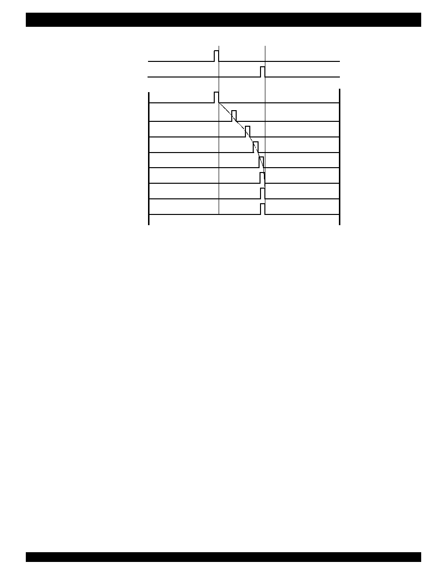
Figure - 6
shows the phase transient that would result if a reference
switch is performed with the TIE Control Block enabled.
Figure - 6 Reference Switch with TIE Control Block Enabled
The phase difference in the Storage Circuit can be cleared by
applying a logic low pulse to the TCLR pin. The reset pulse should be at
least 300 ns.
When the IDT82V3002A primarily enters Holdover Mode for short
time periods and then turns back to Normal Mode, the TIE Control
Circuit should not be enabled. This will prevent undesired accumulated
phase change between the input and output.
If the TIE Control Block is disabled manually or automatically during
the reference switching, the phase of the output signal will align with that
of the new reference. The phase slope is limited to 5 ns per 125 µs.
Figure - 7
shows the phase transient resulting from a reference switch
with the TIE Control Block disabled.
Step Generation
TIE_en
Select
Circuit
Fref0
Fref1
IN_sel
Measure
Circuit
Storage
Circuit
Trigger
Circuit
Feedback
signal
TCLR
Fref
Virtual
Reference
Signal
Input Clock
Fref0
Time = 0.00 s
Time = 0.25 s
Time = 0.50 s
Time = 0.75 s
Time = 1.0 s
Time = 1.25 s
Time = 1.50 s
Time = 1.75 s
Output Clock
Fref1
14
IDT82V3002A WAN PLL WITH DUAL REFERENCE INPUTS INDUSTRIAL TEMPERATURE RANGE
Figure - 7 Reference Switch with TIE Control Block Disabled
3.7
DPLL BLOCK
As shown in
Figure - 8
, the DPLL Block consists of a Phase Detector,
a Limiter, a Loop Filter, a Digital Control Oscillator and Dividers.
Input Clock
Fref0
Fref1
Time = 0.00 s
Time = 0.25 s
Time = 0.50 s
Time = 0.75 s
Time = 1.0 s
Time = 1.25 s
Time = 1.50 s
Time = 1.75 s
Output Clock

15
IDT82V3002A WAN PLL WITH DUAL REFERENCE INPUTS INDUSTRIAL TEMPERATURE RANGE
Figure - 8 DPLL Block Diagram
3.7.1
PHASE DETECTOR (PHD)
In Normal Mode, the Phase Detector compares the virtual reference
signal from the TIE Control Circuit with the feedback signal from the
Frequency Select Circuit, and outputs an error signal corresponding to
the phase difference between the two. This error signal is then sent to
the Limiter circuit for phase slope control.
The feedback signal can be 8 kHz, 2.048 MHz or 1.544 MHz, as
selected by F_sel1 and F_sel0 pins. Refer to
Table - 3
for details.
In Freerun or Holdover Mode, the Frequency Select Circuit, the
Phase Detector and the Limiter are not active and the input reference
signals are not used.
3.7.2
LIMITER
The Limiter is used to ensure that the DPLL responds to all input
transient conditions with a maximum output phase slope of 5 ns per 125
µs. This well meets AT&T TR62411 and Telcordia GR-1244-CORE
specifications, which specify the maximum phase slope of 7.6 ns per
125 µs and 81 ns per 1.326 ms respectively.
In Normal Mode, the Limiter receives the error signal from the Phase
Detector, limits the phase slope within 5 ns per 125 µs and sends the
limited signal to the Loop Filter.
The fast lock mode is a submode of Normal Mode. By setting the
FLOCK pin to high, the device will enter fast lock mode. In this mode,
the Limiter is disabled and the DPLL will lock to the incoming reference
within 500 ms.
3.7.3
LOOP FILTER
The Loop Filter ensures that the jitter transfer meets ETS 300 011
and AT&T TR62411 requirements. This Loop Filter works similarly to a
first order low pass filter with 2.1 Hz cutoff frequency for the three valid
input reference signals (8 kHz, 2.048 MHz or 1.544 MHz).
The output of the Loop Filter goes to the Digital Control Oscillator
directly or via the Fraction blocks, in which E1, T1 and C6 signals are
generated.
3.7.4
FRACTION BLOCK
By applying some algorithms to the incoming E1 signal, the
Fraction_C6 and Fraction_T1 blocks generate C6 and T1 signals
respectively.
3.7.5
DIGITAL CONTROL OSCILLATOR (DCO)
In Normal Mode, the DCO receives three limited and filtered signals
from Loop Filter or Fraction blocks. Based on the received signals, the
DCO generates three digital outputs, 25.248 MHz, 32.768 MHz and
Di
gital Contr
o
l Oscillator
C32o
C16o
C8o
C4o
C2o
C3o
C6o
F0o
F8o
RSP
TSP
F16o
C1.5o
F32o
Output Interface
T1_Divider
E1_Divider
C6_Divider
Frequency
Selection
Circuit
Phase
Detector
Virtual Reference
Loop Filter
Fraction_C6
Fraction_T1
24.704 MHz
32.768 MHz
25.248 MHz
Feedback
Signal
Limiter
FLOCK
F_sel1 F_sel0

16
IDT82V3002A WAN PLL WITH DUAL REFERENCE INPUTS INDUSTRIAL TEMPERATURE RANGE
24.704 MHz for C6, E1 and T1 divider respectively.
In Holdover mode, the DCO is running at the same frequency which
is generated by using the storage techniques.
In Freerun mode, the DCO is running at the same frequency as that
of the master clock.
3.7.6
LOCK INDICATOR
In Normal Mode, the LOCK pin will be set to high only when the
following equation is satisfied:
|f
out
≠ f
in
|
0.4 ppm
f
out
= the average frequency of the output clock signal from the DPLL
(within 2 seconds)
f
in
= the average frequency of the input reference (within 2 seconds)
In other operation modes, the LOCK pin remains low.
3.7.7
OUTPUT INTERFACE
The Output Interface uses three output signals of the DCO to
generate eight types of clock signals and six types of framing signals
totally.
The 32.768 MHz signal is used by the E1_divider to generate five
types of clock signals (C2o, C4o, C8o, C16o and C32o) with nominal
50% duty cycle and six types of framing signals (F0o, F8o, F16o, F32o,
RSP and TSP).
The 24.704 MHz signal is used by the T1_divider to generate two
types of T1 signals (C1.5o and C3o) with nominal 50% duty cycle.
The 25.248 MHz signal is used by the C6_divider to generate a C6o
signal with nominal 50% duty cycle.
All these output signals are synchronous to F8o.
3.8
OSC
The IDT82V3002A can use a clock as the master timing source.
In Freerun Mode, the frequency tolerance at the clock outputs is
identical to that of the source at the OSCi pin. For applications not
requiring an accurate Freerun Mode, the tolerance of the master timing
source may be ±100 ppm. For applications requiring an accurate
Freerun Mode, such as AT&T TR62411, the tolerance of the master
timing source must be no greater than ±32 ppm.
The desired capture range should be taken into consideration when
determining the accuracy of the master timing source. The sum of the
accuracy of the master timing source and the capture range of the
IDT82V3002A will always equal 230 ppm. For example, if the master
timing source is 100 ppm, the capture range will be 130 ppm.
3.8.1
CLOCK OSCILLATOR
When selecting a clock oscillator, numerous parameters must be
considered, including absolute frequency, frequency change over
temperature, output rise and fall times, output levels and duty cycle.
For applications requiring ±32 ppm clock accuracy, the following
clock oscillator module may be used.
FOX F7C-2E3-20.0 MHz
Frequency:
20 MHz
Tolerance:
25 ppm 0∞C to 70∞C
Rise & Fall Time:10 ns (0.33 V 2.97 V 15 pF)
Duty Cycle:
40% to 60%
The output clock should be connected directly (not AC coupled) to
the OSCi input of the IDT82V3002A, and the OSCo output should be left
open as shown in
Figure - 9
.
Figure - 9 Clock Oscillator Circuit
3.9
JTAG
The IDT82V3002A supports IEEE 1149.1 JTAG Scan.
3.10
RESET CIRCUIT
A simple power up reset circuit is shown in
Figure - 10
. Resistor Rp is
used for protection only and limits current into the RST pin during power
down conditions. The reset low time is not critical but should be greater
than 300 ns. In
Figure - 10
,
the reset low time is about 50 µs.
Figure - 10 Power-Up Reset Circuit
+3.3 V
20 MHz OUT
GND
+3.3 V
No Connection
OSCo
OSCi
IDT82V3002A
0.1
µF
3.3 V
R
10 k
Rp
1 k
C
1
µF
RST
IDT82V3002A

17
IDT82V3002A WAN PLL WITH DUAL REFERENCE INPUTS INDUSTRIAL TEMPERATURE RANGE
4
MEASURES OF PERFOR-
MANCE
The following are some synchronizer performance indicators and
their corresponding definitions.
4.1
INTRINSIC JITTER
Intrinsic jitter is the jitter produced by the synchronizing circuit and is
measured at its output. It is measured by applying a reference signal
with no jitter to the input of the device, and measuring its output jitter.
Intrinsic jitter may also be measured when the device is in a non-
synchronizing mode, such as free running or holdover, by measuring the
output jitter of the device. Intrinsic jitter is usually measured with various
band limiting filters depending on the applicable standards. In the
IDT82V3002A, the intrinsic Jitter is limited to less than 0.02 UI on the
2.048 MHz and 1.544 MHz clocks.
4.2
JITTER TOLERANCE
Jitter tolerance is a measure of the ability of a DPLL to operate
properly (i.e., remain in lock and or regain lock in the presence of large
jitter magnitudes at various jitter frequencies) when jitter is applied to its
reference. The applied jitter magnitude and jitter frequency depends on
the applicable standards.
4.3
JITTER TRANSFER
Jitter transfer or jitter attenuation refers to the magnitude of jitter at
the output of a device for a given amount of jitter at the input of the
device. Input jitter is applied at various amplitudes and frequencies, and
output jitter is measured with various filters depending on the applicable
standards.
For the IDT82V3002A, two internal elements determine the jitter
attenuation. This includes the internal 2.1 Hz low pass loop filter and the
phase slope limiter. The phase slope limiter limits the output phase
slope to 5 ns/125 µs. Therefore, if the input signal exceeds this rate,
such as for very large amplitude low frequency input jitter, the maximum
output phase slope will be limited (i.e., attenuated) to 5 ns/125 µs.
The IDT82V3002A has fourteen outputs with three possible input
frequencies for a total of 39 possible jitter transfer functions. Since all
outputs are derived from the same signal, the jitter transfer values for
three cases, 8 kHz to 8 kHz, 1.544 MHz to 1.544 MHz and 2.048 MHz to
2.048 MHz can be applied to all outputs.
It should be noted that 1 UI at 1.544 MHz is 644 ns, which is not
equal to 1 UI at 2.048 MHz, which is 488 ns. Consequently, a transfer
value using different input and output frequencies must be calculated in
common units (e.g., seconds).
Using the above method, the jitter attenuation can be calculated for
all combinations of inputs and outputs based on the three jitter transfer
functions provided. Note that the resulting jitter transfer functions for all
combinations of inputs (8 kHz, 1.544 MHz, 2.048 MHz) and outputs (8
kHz, 1.544 MHz, 3.088 MHz, 6.312 MHz, 2.048 MHz, 4.096 MHz, 8.192
MHz, 16.384 MHz, 32.768 MHz) for a given input signal (jitter frequency
and jitter amplitude) are the same.
Since intrinsic jitter is always present, jitter attenuation will appear to
be lower for small input jitter signals than for large ones. Consequently,
accurate jitter transfer function measurements are usually made with
large input jitter signals (e.g., 75% of the specified maximum jitter
tolerance).
4.4
FREQUENCY ACCURACY
Frequency accuracy is defined as the absolute tolerance of an output
clock signal when it is not locked to an external reference, but is
operating in a free running mode. For the IDT82V3002A, the Freerun
accuracy is equal to the Master Clock (OSCi) accuracy.
4.5
HOLDOVER ACCURACY
Holdover accuracy is defined as the absolute tolerance of an output
clock signal, when it is not locked to an external reference signal, but is
operating using storage techniques. For the IDT82V3002A, the storage
value is determined while the device is in Normal Mode and locked to an
external reference signal.
The absolute Master Clock (OSCi) accuracy of the IDT82V3002A
does not affect Holdover accuracy, but the change in OSCi accuracy
while in Holdover Mode does.
4.6
CAPTURE RANGE
Also referred to as pull-in range. This is the input frequency range
over which the synchronizer must be able to pull into synchronization.
The IDT82V3002A capture range is equal to ±230 ppm minus the
accuracy of the master clock (OSCi). For example, a 32 ppm master
clock results in a capture range of 198 ppm.
The Telcordia GR-1244-CORE standard, recommends that the DPLL
should be able to reject references that are off the nominal frequency by
more than ±12 ppm. The IDT82V3002A provides one pin, MON_out, to
indicate whether the primary reference are within ±12 ppm of the
nominal frequency.
4.7
LOCK RANGE
This is the input frequency range over which the synchronizer must
be able to maintain synchronization. The lock range is equal to the
capture range for the IDT82V3002A.
4.8
PHASE SLOPE
Phase slope is measured in seconds per second and is the rate at
which a given signal changes phase with respect to an ideal signal. The
given signal is typically the output signal. The ideal signal is of constant
frequency and is nominally equal to the value of the final output signal or
final input signal.
4.9
TIME INTERVAL ERROR (TIE)
TIE is the time delay between a given timing signal and an ideal
timing signal.
4.10
MAXIMUM TIME INTERVAL ERROR (MTIE)
MTIE is the maximum peak to peak delay between a given timing
signal and an ideal timing signal within a particular observation period.

18
IDT82V3002A WAN PLL WITH DUAL REFERENCE INPUTS INDUSTRIAL TEMPERATURE RANGE
4.11
PHASE CONTINUITY
Phase continuity is the phase difference between a given timing
signal and an ideal timing signal at the end of a particular observation
period. Usually, the given timing signal and the ideal timing signal are of
the same frequency. Phase continuity applies to the output of the
synchronizer after a signal disturbance due to a mode change. The
observation period is usually the time from the disturbance, to just after
the synchronizer has settled to a steady state.
In the case of the IDT82V3002A, the output signal phase continuity is
maintained to within ±5 ns at the instance (over one frame) of all mode
changes. The total phase shift, depending on the type of mode change,
may accumulate up to 200 ns over many frames. The rate of change of
the 200 ns phase shift is limited to a maximum phase slope of
approximately 5 ns/125 µs. This meets AT&T TR62411 maximum
phase slope requirement of 7.6 ns/125 µs and Telcordia GR-1244-
CORE (81 ns/1.326 ms).
4.12
PHASE LOCK TIME
This is the time it takes the synchronizer to phase lock to the input
signal. Phase lock occurs when the input signal and output signal are
not changing in phase with respect to each other (not including jitter).
Lock time is very difficult to determine because it is affected by many
factors, which include:
i) Initial input to output phase difference
ii) Initial input to output frequency difference
iii) Synchronizer loop filter
iv) Synchronizer limiter
Although a short lock time is desirable, it is not always possible to
achieve due to other synchronizer requirements. For instance, better
jitter transfer performance is achieved with a lower frequency loop filter
which increases lock time. And better (smaller) phase slope
performance (limiter) results in longer lock times. The IDT82V3002A
loop filter and limiter were optimized to meet the AT&T TR62411 jitter
transfer and phase slope requirements. Consequently, phase lock time,
which is not a standards requirement, may be longer than in other
applications. See
Table - 8
for Maximum Phase Lock Time.
The IDT82V3002A provides a fast lock pin (FLOCK), which enables
the DPLL to lock to an incoming reference within approximately 500 ms
when set high.

19
IDT82V3002A WAN PLL WITH DUAL REFERENCE INPUTS INDUSTRIAL TEMPERATURE RANGE
5
TEST SPECIFICATIONS
Note:
Stresses greater than those listed under ABSOLUTE MAXIMUM RATINGS may cause permanent damage to the device. This is a stress rating only and functional operation of the device
at these or any other conditions above those indicated in the operational sections of this specification is not implied. Exposure to absolute maximum rating conditions for extended periods
may affect reliability.
Table - 5 Absolute Maximum Ratings**
Rating
Min.
Max.
Unit
Power Supply Voltage
-0.5
5.0
V
Voltage on Any Pin with Respect to Ground
-0.5
V
DD
+ 0.5
V
Package Power Dissipation
200
mW
Storage Temperature
-55
125
∞C
Table - 6 Recommended DC Operating Conditions**
Parameter
Min.
Typ.
Max.
Unit
Operating Temperature
-40
+85
∞C
Power Supply Voltage
3.0
3.6
V
Table - 7 DC Electrical Characteristics**
Parameter
Description
Min
Typ.
Max
Units
Test Conditions
I
DDS
Supply current with OSCi = 0 V
10
mA
Outputs unloaded
I
DD
Supply current with OSCi = Clock
60
mA
Outputs unloaded
V
CIH
CMOS high-level input voltage
0.7V
DD
V
OSCi, Fref0 and Fref1
V
CIL
CMOS low-level input voltage
0.3V
DD
V
OSCi, Fref0 and Fref1
V
TIH
TTL high-level input voltage
2.0
V
All input pins except for OSCi, Fref0 and Fref1
V
TIL
TTL low-level input voltage
0.8
V
All input pins except for OSCi, Fref0 and Fref1
I
IL
Input leakage current:
µA
V
I
= V
DD
or 0 V
Normal (low level)
-15
15
Normal (high level)
-15
15
Pull up (low level)
-100
0
Pull up (high level)
-15
15
Pull down (low level)
-15
15
Pull down (high level)
0
100
V
OH
High-level output voltage
2.4
V
I
OH
= 8 mA
V
OL
Low-level output voltage
0.4
V
I
OL
= 8 mA

20
IDT82V3002A WAN PLL WITH DUAL REFERENCE INPUTS INDUSTRIAL TEMPERATURE RANGE
5.1
AC ELECTRICAL CHARACTERISTICS
**Note:
Voltages are with respect to ground (V
ss
) unless otherwise stated.
Table - 8 Performance**
Description
Min
Typ.
Max
Units
Test Conditions / Notes*
Freerun Mode accuracy with OSCi at : 0 ppm
-0
+0
ppm
5-8
Freerun Mode accuracy with OSCi at : ±32 ppm
-32
+32
ppm
5-8
Freerun Mode accuracy with OSCi at : ±100 ppm
-100
+100
ppm
5-8
Holdover Mode accuracy with OSCi at : 0 ppm
-0.025
+0.025
ppm
1, 2, 4, 6-8, 40, 41
Holdover Mode accuracy with OSCi at : ±32 ppm
-0.025
+0.025
ppm
1, 2, 4, 6-8, 40, 41
Holdover Mode accuracy with OSCi at : ±100 ppm
-0.025
+0.025
ppm
1, 2, 4, 6-8, 40, 41
Capture range with OSCi at : 0 ppm
-230
+230
ppm
1-3, 6-8
Capture range with OSCi at : ±32 ppm
-198
+198
ppm
1-3, 6-8
Capture range with OSCi at : ±100 ppm
-130
+130
ppm
1-3, 6-8
Phase lock time
50
s
1-3, 6-14, 42
Output phase continuity with reference switch
200
ns
1-3, 6-14
Output phase continuity with mode switch to Normal
200
ns
1-2, 4-14
Output phase continuity with mode switch to Freerun
200
ns
1-2, 5-14
Output phase continuity with mode switch to Holdover
50
ns
1-3, 6-14
MON_out is low level - Reference frequency accuracy must be:
-12
+12
ppm
MTIE (maximum time interval error)
600
ns
1-14, 27
Output phase slope
40
µs/s
1-14, 27
Reference input for Auto-Holdover with 8 kHz
-18 k
+18 k
ppm
1-3, 6, 9-11
Reference input for Auto-Holdover with 1.544 MHz
-36 k
+36 k
ppm
1-3, 7, 9-11
Reference input for Auto-Holdover with 2.048 MHz
-36 k
+36 k
ppm
1-3, 8, 9-11
Table - 9 Intrinsic Jitter Unfiltered
Description
Min
Typ
Max
Units
Test Conditions / Notes*
Intrinsic jitter at F8o ( 8 kHz )
0.0001
UIpp
1-14, 21-24, 28
Intrinsic jitter at F0o ( 8 kHz )
0.0001
UIpp
1-14, 21-24, 28
Intrinsic jitter at F16o ( 8 kHz )
0.0001
UIpp
1-14, 21-24, 28
Intrinsic jitter at C1.5o ( 1.544 MHz )
0.015
UIpp
1-14, 21-24, 29
Intrinsic jitter at C3o ( 3.088 MHz )
0.03
UIpp
1-14, 21-24, 31
Intrinsic jitter at C2o ( 2.048 MHz )
0.01
UIpp
1-14, 21-24, 30
Intrinsic jitter at C6o ( 6.312 MHz )
0.06
UIpp
1-14, 21-24
Intrinsic jitter at C4o ( 4.096 MHz )
0.02
UIpp
1-14, 21-24, 32
Intrinsic jitter at C8o ( 8.192 MHz )
0.04
UIpp
1-14, 21-24, 33
Intrinsic jitter at C16o ( 16.834 MHz )
0.04
UIpp
1-14, 21-24, 34
Intrinsic jitter at TSP ( 8 kHz )
0.0001
UIpp
1-14, 21-24, 34
Intrinsic jitter at RSP ( 8 kHz )
0.0001
UIpp
1-14, 21-24, 34
Intrinsic jitter at C32o ( 32.768 MHz )
0.08
UIpp
1-14, 21-24, 35

21
IDT82V3002A WAN PLL WITH DUAL REFERENCE INPUTS INDUSTRIAL TEMPERATURE RANGE
Table - 10 C1.5o (1.544 MHz) Intrinsic Jitter Filtered
Description
Min
Typ
Max
Units
Test Conditions / Notes*
Intrinsic jitter (4 Hz to 100 kHz filter)
0.008
UIpp
1-14, 21-24, 29
Intrinsic jitter (10 Hz to 40 kHz filter)
0.006
UIpp
1-14, 21-24, 29
Intrinsic jitter (8 kHz to 40 kHz filter)
0.006
UIpp
1-14, 21-24, 29
Intrinsic jitter (10 Hz to 8 kHz filter)
0.003
UIpp
1-14, 21-24, 29
Table - 11 C2o (2.048 MHz) Intrinsic Jitter Filtered
Description
Min
Typ
Max
Units
Test Conditions / Notes*
Intrinsic jitter (4 Hz to 100 kHz filter)
0.005
UIpp
1-14, 21-24, 30
Intrinsic jitter (10 Hz to 40 kHz filter)
0.004
UIpp
1-14, 21-24, 30
Intrinsic jitter (8 kHz to 40 kHz filter)
0.003
UIpp
1-14, 21-24, 30
Intrinsic jitter (10 Hz to 8 kHz filter)
0.002
UIpp
1-14, 21-24, 30
Table - 12 8 kHz Input to 8 kHz Output Jitter Transfer
Description
Min
Typ
Max
Units
Test Conditions / Notes*
Jitter attenuation for 1 Hz@0.01 UIpp input
0
6
dB
1-3, 6, 9-14, 21-22, 24, 28, 35
Jitter attenuation for 1 Hz@0.54 UIpp input
6
16
dB
1-3, 6, 9-14, 21-22, 24, 28, 35
Jitter attenuation for 10 Hz@0.10 UIpp input
15
22
dB
1-3, 6, 9-14, 21-22, 24, 28, 35
Jitter attenuation for 60 Hz@0.10 UIpp input
32
38
dB
1-3, 6, 9-14, 21-22, 24, 28, 35
Jitter attenuation for 300 Hz@0.10 UIpp input
42
dB
1-3, 6, 9-14, 21-22, 24, 28, 35
Jitter attenuation for 3600 Hz@0.005 UIpp input
50
dB
1-3, 6, 9-14, 21-22, 24, 28, 35
Table - 13 1.544 MHz Input to 1.544 MHz Output Jitter Transfer
Description
Min
Typ
Max
Units
Test Conditions / Notes*
Jitter attenuation for 1 Hz@20 UIpp input
0
6
dB
1-3, 7, 9-14, 21-22, 24, 29, 35
Jitter attenuation for 1 Hz@104 UIpp input
6
16
dB
1-3, 7, 9-14, 21-22, 24, 29, 35
Jitter attenuation for 10 Hz@20 UIpp input
17
22
dB
1-3, 7, 9-14, 21-22, 24, 29, 35
Jitter attenuation for 60 Hz@20 UIpp input
33
38
dB
1-3, 7, 9-14, 21-22, 24, 29, 35
Jitter attenuation for 300 Hz@20 UIpp input
45
dB
1-3, 7, 9-14, 21-22, 24, 29, 35
Jitter attenuation for 10 kHz@0.3 UIpp input
48
dB
1-3, 7, 9-14, 21-22, 24, 29, 35
Jitter attenuation for 40 kHz@0.3 UIpp input
50
dB
1-3, 7, 9-14, 21-22, 24, 29, 35

22
IDT82V3002A WAN PLL WITH DUAL REFERENCE INPUTS INDUSTRIAL TEMPERATURE RANGE
Table - 14 2.048 MHz Input to 2.048 MHz Output Jitter Transfer
Description
Min
Typ
Max
Units
Test Conditions / Notes*
Jitter at output for 1 Hz@3.00 UIpp input
2.5
UIpp
1-3, 8, 9-14, 21-22, 24, 30, 35
Jitter at output for 1 Hz@3.00 UIpp input with 40 Hz to 100 Hz filter
0.07
UIpp
1-3, 8, 9-14, 21-22, 24, 30, 36
Jitter at output for 3 Hz@2.33 UIpp input
1.4
UIpp
1-3, 8, 9-14, 21-22, 24, 30, 35
Jitter at output for 3 Hz@2.33 UIpp input with 40 Hz to 100 Hz filter
0.10
UIpp
1-3, 8, 9-14, 21-22, 24, 30, 36
Jitter at output for 5 Hz@2.07 UIpp input
0.90
UIpp
1-3, 8, 9-14, 21-22, 24, 30, 35
Jitter at output for 5 Hz@2.07 UIpp input with 40 Hz to 100 Hz filter
0.10
UIpp
1-3, 8, 9-14, 21-22, 24, 30, 36
Jitter at output for 10 Hz@1.76 UIpp input
0.40
UIpp
1-3, 8, 9-14, 21-22, 24, 30, 35
Jitter at output for 10 Hz@1.76 UIpp input with 40 Hz to 100 Hz filter
0.10
UIpp
1-3, 8, 9-14, 21-22, 24, 30, 36
Jitter at output for 100 Hz@1.50 UIpp input
0.06
UIpp
1-3, 8, 9-14, 21-22, 24, 30, 35
Jitter at output for 100 Hz@1.50 UIpp input with 40 Hz to 100 Hz filter
0.05
UIpp
1-3, 8, 9-14, 21-22, 24, 30, 36
Jitter at output for 2400 Hz@1.50 UIpp input
0.04
UIpp
1-3, 8, 9-14, 21-22, 24, 30, 35
Jitter at output for 2400 Hz@1.50 UIpp input with 40 Hz to 100 Hz filter
0.03
UIpp
1-3, 8, 9-14, 21-22, 24, 30, 36
Jitter at output for 100 kHz@0.20 UIpp input
0.04
UIpp
1-3, 8, 9-14, 21-22, 24, 30, 35
Jitter at output for 100 kHz@0.20 UIpp input with 40 Hz to 100 Hz filter
0.02
UIpp
1-3, 8, 9-14, 21-22, 24, 30
Table - 15 8 kHz Input Jitter Tolerance
Description
Min
Typ
Max
Units
Test Conditions / Notes*
Jitter tolerance for 1 Hz input
0.80
UIpp
1-3, 6, 9-14, 21-22, 24-26, 28
Jitter tolerance for 5 Hz input
0.70
UIpp
1-3, 6, 9-14, 21-22, 24-26, 28
Jitter tolerance for 20 Hz input
0.60
UIpp
1-3, 6, 9-14, 21-22, 24-26, 28
Jitter tolerance for 300 Hz input
0.16
UIpp
1-3, 6, 9-14, 21-22, 24-26, 28
Jitter tolerance for 400 Hz input
0.14
UIpp
1-3, 6, 9-14, 21-22, 24-26, 28
Jitter tolerance for 700 Hz input
0.07
UIpp
1-3, 6, 9-14, 21-22, 24-26, 28
Jitter tolerance for 2400 Hz input
0.02
UIpp
1-3, 6, 9-14, 21-22, 24-26, 28
Jitter tolerance for 3600 Hz input
0.01
UIpp
1-3, 6, 9-14, 21-22, 24-26, 28
Table - 16 1.544 MHz Input Jitter Tolerance
Description
Min
Typ
Max
Units
Test Conditions / Notes*
Jitter tolerance for 1 Hz input
150
UIpp
1-3, 7, 9-14, 21-22, 24-26, 29
Jitter tolerance for 5 Hz input
140
UIpp
1-3, 7, 9-14, 21-22, 24-26, 29
Jitter tolerance for 20 Hz input
130
UIpp
1-3, 7, 9-14, 21-22, 24-26, 29
Jitter tolerance for 300 Hz input
38
UIpp
1-3, 7, 9-14, 21-22, 24-26, 29
Jitter tolerance for 400 Hz input
25
UIpp
1-3, 7, 9-14, 21-22, 24-26, 29
Jitter tolerance for 700 Hz input
15
UIpp
1-3, 7, 9-14, 21-22, 24-26, 29
Jitter tolerance for 2400 Hz input
5
UIpp
1-3, 7, 9-14, 21-22, 24-26, 29
Jitter tolerance for 10 kHz input
1.2
UIpp
1-3, 7, 9-14, 21-22, 24-26, 29
Jitter tolerance for 40 kHz input
0.5
UIpp
1-3, 7, 9-14, 21-22, 24-26, 29

23
IDT82V3002A WAN PLL WITH DUAL REFERENCE INPUTS INDUSTRIAL TEMPERATURE RANGE
*
Notes:
Voltages are with respect to ground (V
SS
) unless otherwise stated.
Supply voltage and operating temperature are as per Recommended Operating Conditions.
Timing parameters are as per AC Electrical Characteristics - Timing Parameter Measurement Voltage Levels
1.
Fref0 reference input selected.
2.
Fref1 reference input selected.
3.
Normal Mode selected.
4.
Holdover Mode selected.
5.
Freerun Mode selected.
6.
8 kHz Frequency Mode selected.
7.
1.544 MHz Frequency Mode selected.
8.
2.048 MHz Frequency Mode selected.
9.
Master clock input OSCi at 20 MHz ±0 ppm.
10. Master clock input OSCi at 20 MHz ±32 ppm.
11. Master clock input OSCi at 20 MHz ±100 ppm.
12. Selected reference input at
±0 ppm.
13. Selected reference input at
±32 ppm.
14. Selected reference input at
±100 ppm.
15. For Freerun Mode of
±0 ppm.
16. For Freerun Mode of
±32 ppm.
17. For Freerun Mode of
±100 ppm.
18. For capture range of
±230 ppm.
19. For capture range of
±198 ppm.
20. For capture range of
±130 ppm.
21. 25 pF capacitive load.
22. OSCi Master Clock jitter is less than 2 nspp, or 0.04 UIpp where 1 UIpp = 1/20 MHz.
23. Jitter on reference input is obtained at slightly higher input jitter amplitudes.
24. Applied jitter is sinusoidal.
25. Minimum applied input jitter magnitude to regain synchronization.
26. Loss of synchronization is obtained at slightly higher input jitter amplitudes.
27. Within 10 ms of the state, reference or input change.
28. 1 UIpp = 125 µs for 8 kHz signals.
29. 1 UIpp = 648 ns for 1.544 MHz signals.
30. 1 UIpp = 488 ns for 2.048 MHz signals.
31. 1 UIpp = 323 ns for 3.088 MHz signals.
32. 1 UIpp = 244 ns for 4.096 MHz signals.
33. 1 UIpp = 122 ns for 8.192 MHz signals.
34. 1 UIpp = 61 ns for 16.484 MHz signals.
35. 1 UIpp = 30 ns for 32.968 MHz signals.
36. No filter.
37. 40 Hz to 100 kHz bandpass filter.
38. With respect to reference input signal frequency.
39. After chip reset or TIE reset.
40. Master clock duty 40% to 60%.
41. Prior to Holdover Mode, device as in Normal Mode and phase locked.
42. With input frequency offset of 100 ppm.
Table - 17 2.048 MHz Input Jitter Tolerance
Description
Min
Typ
Max
Units
Test Conditions / Notes*
Jitter tolerance for 1 Hz input
150
UIpp
1-3, 8, 9-14, 21-22, 24-26, 30
Jitter tolerance for 5 Hz input
140
UIpp
1-3, 8, 9-14, 21-22, 24-26, 30
Jitter tolerance for 20 Hz input
130
UIpp
1-3, 8, 9-14, 21-22, 24-26, 30
Jitter tolerance for 300 Hz input
40
UIpp
1-3, 8, 9-14, 21-22, 24-26, 30
Jitter tolerance for 400 Hz input
33
UIpp
1-3, 8, 9-14, 21-22, 24-26, 30
Jitter tolerance for 700 Hz input
18
UIpp
1-3, 8, 9-14, 21-22, 24-26, 30
Jitter tolerance for 2400 Hz input
5.5
UIpp
1-3, 8, 9-14, 21-22, 24-26, 30
Jitter tolerance for 10 kHz input
1.3
UIpp
1-3, 8, 9-14, 21-22, 24-26, 30
Jitter tolerance for 100 kHz input
0.4
UIpp
1-3, 8, 9-14, 21-22, 24-26, 30

24
IDT82V3002A WAN PLL WITH DUAL REFERENCE INPUTS INDUSTRIAL TEMPERATURE RANGE
6
TIMING CHARACTERISTICS
Notes:
1.
Voltages are with respect to ground (V
SS
) unless otherwise stated.
2.
Supply voltage and operating temperature are as per Recommended Operating Conditions.
3.
Timing for input and output signals is based on the worst case result of the CMOS thresholds
Table - 18 Timing Parameter Measurement Voltage Levels
Parameter
Description
CMOS
Units
V
T
Threshold Voltage
0.5V
DD
V
V
HM
Rise and Fall Threshold Voltage High
0.7V
DD
V
V
LM
Rise and Fall Threshold Voltage Low
0.3V
DD
V
Table - 19 Input / Output Timing
Parameter
Description
Min
Typ
Max
Units
Test Conditions
t
RW
Reference input pulse width high or low
100
ns
t
IRF
Reference input rise or fall time
10
ns
t
R8D
8 kHz reference input to F8o delay
0
25
ns
t
R15D
1.544 MHz reference input to F8o delay
326
342
ns
t
R2D
2.048 MHz reference input to F8o delay
248
264
ns
t
FOD
F8o to F0o delay
111
130
ns
t
F16S
F16o setup to C16o falling
25
40
ns
t
F16H
F16o hold to C16o falling
25
40
ns
t
C15D
F8o to C1.5o delay
-10
10
ns
t
C3D
F8o to C3o delay
-10
10
ns
t
C6D
F8o to C6o delay
-10
10
ns
t
C2D
F8o to C2o
-11
5
ns
t
C4D
F8o to C4o
-11
5
ns
t
C8D
F8o to C8o delay
-11
5
ns
t
C16D
F8o to C16o delay
-11
5
ns
t
C32D
F8o to C32o delay
-11
5
ns
t
TSPD
F8o to TSP delay
-6
10
ns
t
RSPD
F8o to RSP delay
-8
8
ns
t
C15W
C1.5o pulse width high or low
309
339
ns
t
C3W
C3o pulse width high or low
154
169
ns
t
C6W
C6o pulse width high or low
70
86
ns
Timing Reference Points
t
IRF,
t
ORF
t
IRF,
t
ORF
V
HM
V
T
V
LM
ALL SIGNALS
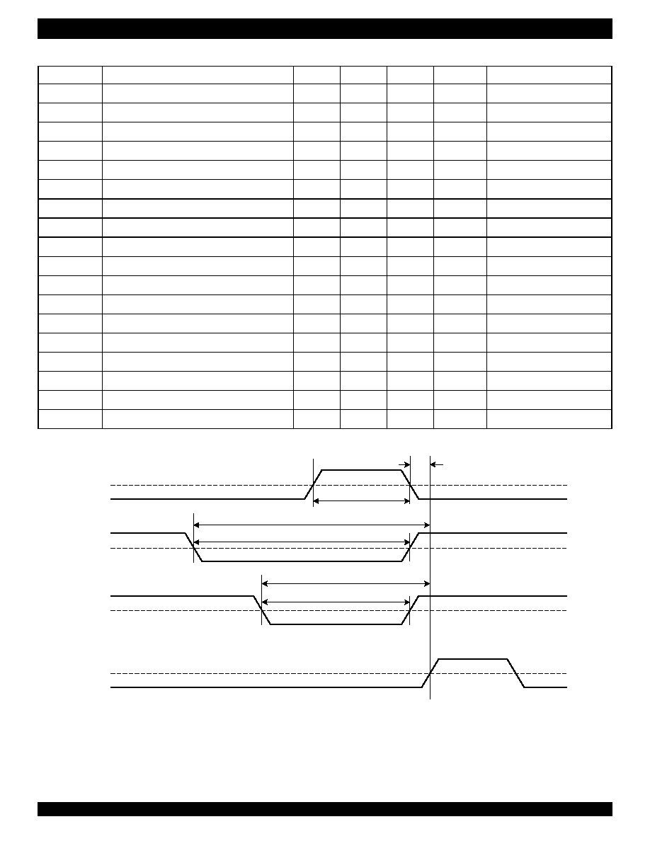
25
IDT82V3002A WAN PLL WITH DUAL REFERENCE INPUTS INDUSTRIAL TEMPERATURE RANGE
Figure - 11 Input to Output Timing (Normal Mode)
t
C2W
C2o pulse width high or low
232
258
ns
t
C4W
C4o pulse width high or low
111
133
ns
t
C8W
C8o pulse width high or low
52
70
ns
t
C16WL
C16o pulse width high or low
24
35
ns
t
C32W
C32o pulse width high or low
14
16.78
ns
t
TSPW
TSP pulse width high
478
494
ns
t
RSPW
RSP pulse width high
474
491
ns
t
F0WL
F0o pulse width low
234
254
ns
t
F8WH
F8o pulse width high
109
135
ns
t
F16WL
F16o pulse width low
47
72
ns
t
0RF
Output clock and frame pulse rise or fall time
9
ns
t
S
Input Controls Setup Time
100
ns
t
H
Input Controls Hold Time
100
ns
t
F16D
F8o to F16o delay
24
38
ns
t
F32D
F8o to F32o delay
12
19
ns
t
F32S
F32o setup to C32o falling
11
ns
t
F32H
F32o hold to C32o falling
11
ns
t
F32WL
F32o pulse width low
15
31
ns
Table - 19 Input / Output Timing (Continued)
Parameter
Description
Min
Typ
Max
Units
Test Conditions
t
R8D
t
RW
t
R15D
t
RW
t
RW
t
R2D
V
T
V
T
V
T
V
T
Fref0/Fref1
8 kHz
Fref0/Fref1
1.544 MHz
Fref0/Fref1
2.048 MHz
F8o

26
IDT82V3002A WAN PLL WITH DUAL REFERENCE INPUTS INDUSTRIAL TEMPERATURE RANGE
Figure - 12 Output Timing 1
t
F8WH
t
F0D
t
F0WL
t
F16D
t
F16WL
t
F16H
t
F16S
t
C16D
t
C16WL
t
C8W
t
C4W
t
C2W
t
C2D
t
C6W
t
C6D
t
C15D
t
C15W
t
C8D
t
C4D
V
T
V
T
V
T
V
T
V
T
V
T
V
T
V
T
V
T
C1.5o
C6o
C2o
C4o
C8o
C16o
F16o
F0o
F8o
C32o
C3o
t
C32D
t
C3D
t
C3W
t
C32W
V
T
V
T
F32o
t
F32WL
t
F32D
V
T
t
F32S
t
F32H
t
C6W
t
C4W
t
C8W
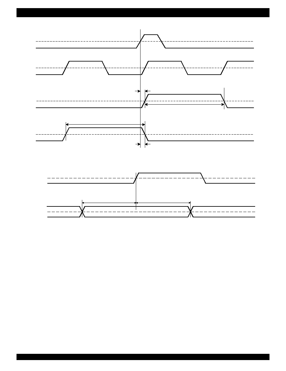
27
IDT82V3002A WAN PLL WITH DUAL REFERENCE INPUTS INDUSTRIAL TEMPERATURE RANGE
Figure - 13 Output Timing 2
Figure - 14 Input Control Setup and Hold Timing
F8o
C2o
RSP
TSP
t
RSPD
t
RSPW
t
TSPD
t
TSPW
V
T
V
T
V
T
V
T
V
T
V
T
t
H
t
S
F8o
MODE_sel0
MODE_sel1
TIE_en
IN_sel

IDT82V3002A WAN PLL WITH DUAL REFERENCE INPUTS INDUSTRIAL TEMPERATURE RANGE
28
CORPORATE HEADQUARTERS
2975 Stender Way
Santa Clara, CA 95054
for SALES:
800-345-7015 or 408-727-6116
fax: 408-492-8674
www.idt.com
for Tech Support:
email: telecomhelp@idt.com
phone: 408-330-1753
7
ORDERING INFORMATION
IDT
XXXXXXX
XX
X
Device Type
Blank
Process/
Temperature
Range
82V3002A
Industrial (-40 ∞C to +85 ∞C)
WAN PLL with Dual Reference Inputs
Package
PV
Shrink Small Outline Package (SSOP, PV56)