
COMMERCIAL TEMPERATURE RANGE
IDT74FCT863A/B
HIGH-PERFORMANCE CMOS 9-BIT NON-INVERTING TRANSCEIVER
1
JULY 2000
COMMERCIAL TEMPERATURE RANGE
The IDT logo is a registered trademark of Integrated Device Technology, Inc.
© 2000 Integrated Device Technology, Inc.
DSC-5424/1
FEATURES:
∑ Equivalent to AMD's Am29861-64 bipolar registers in pinout/
function, speed, and output drive over full temperature and
voltage supply extremes
∑ IDT74FCT863A equivalent to FASTTM speed
∑ IDT74FCT863B 25% faster than FAST
∑ High-speed symmetrical bidirectional transceivers
∑ I
OL
= 48mA
∑ Clamp diodes on all inputs for ringing suppression
∑ CMOS power levels (1mW typ. static)
∑ TTL input and output level compatible
∑ CMOS output level compatible
∑ Substantially lower input current levels than AMD's bilopar
Am29800 series (5
µµ
µµ
µA max.)
∑ Available in SOIC package
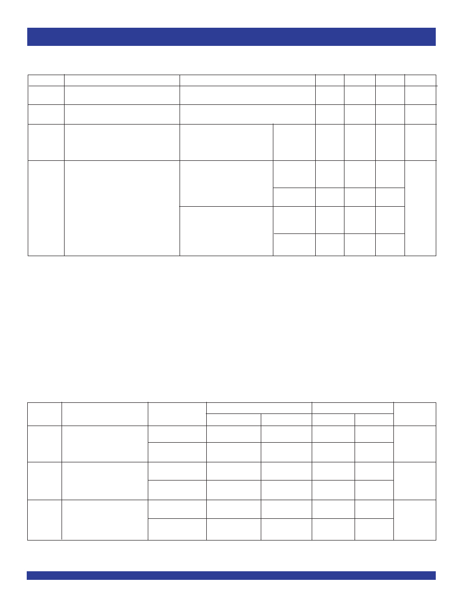
FUNCTIONAL BLOCK DIAGRAM
IDT74FCT863A/B
HIGH-PERFORMANCE
CMOS 9-BIT NON-INVERTING
TRANSCEIVER
DESCRIPTION:
The IDT74FCT800 series is built using an advanced dual metal CMOS
technology. The IDT74FCT863 9-bit transceivers have NAND-ed output
enables for maximum control flexibility.
All of the IDT74FCT800 high-performance interface family is designed
for high-capacitance load drive capability while providing low-capacitance
bus loading at both inputs and outputs. All inputs have clamp diodes and
all outputs are designed for low-capacitance bus loading in the high-
impedance state.
R
1
- R
8
R
0
T
0
T
1
- T
8
OET
1
OET
2
OER
1
OER
2

COMMERCIAL TEMPERATURE RANGE
2
IDT74FCT863A/B
HIGH-PERFORMANCE CMOS 9-BIT NON-INVERTING TRANSCEIVER
PIN CONFIGURATION
Symbol
Description
Max
Unit
V
TERM
(2)
Terminal Voltage with Respect to GND
≠0.5 to +7
V
V
TERM
(3)
Terminal Voltage with Respect to GND
≠0.5 to V
CC
V
T
A
Operating Temperature
0 to +70
∞C
T
BIAS
Temperature under BIAS
≠55 to +125
∞C
T
STG
Storage Temperature
≠55 to +125
∞C
P
T
Power Dissipation
0.5
W
I
OUT
DC Output Current
120
mA
ABSOLUTE MAXIMUM RATINGS
(1)
NOTES:
1. Stresses greater than those listed under ABSOLUTE MAXIMUM RATINGS may cause
permanent damage to the device. This is a stress rating only and functional operation
of the device at these or any other conditions above those indicated in the operational
sections of this specification is not implied. Exposure to absolute maximum rating
conditions for extended periods may affect reliability. No terminal voltage may exceed
Vcc by +0.5V unless otherwise noted.
2. Input and Vcc terminals only.
3. Output and I/O terminals only.
SOIC
TOP VIEW
Symbol
Parameter
(1)
Conditions
Typ.
Max.
Unit
C
IN
Input Capacitance
V
IN
= 0V
6
10
pF
C
OUT
Output Capacitance
V
OUT
= 0V
8
12
pF
CAPACITANCE
(T
A
= +25∞C, F = 1.0MHz)
NOTE:
1. This parameter is measured at characterization but not tested.
R
T
9
9
OET
1
OET
2
OER
1
OER
2
LOGIC SYMBOL
2
3
1
20
19
18
15
16
23
22
24
21
17
V
CC
OET
1
13
14
T
6
T
7
T
2
T
5
T
3
T
4
T
8
T
0
T
1
OET
2
9
10
R
6
R
7
R
2
R
5
R
3
R
4
R
8
5
6
7
4
8
R
0
OER
1
11
12
R
1
GND
OER
2
PIN DESCRIPTION
Name
I/O
Description
OER
I
I
When LOW in conjunction with OET
I
HIGH
activates the RECEIVE mode.
OET
I
I
When LOW in conjunction with OER
I
HIGH
activates the TRANSMIT mode.
R
I
I/O
9-bit RECEIVE input/output.
T
I
I/O
9-bit TRANSMIT input/output.
FUNCTION TABLE
(1)
Inputs
Outputs
OET
OER
R
I
T
I
R
I
T
I
Function
L
H
L
N/A
N/A
L
Transmitting
L
H
H
N/A
N/A
H
Transmitting
H
L
N/A
L
L
N/A
Receiving
H
L
N/A
H
H
N/A
Receiving
H
H
X
X
Z
Z
High Z
NOTE:
1. H = HIGH
L = LOW
Z = High Impedance
X = Don't Care
N/A = Not Applicable

COMMERCIAL TEMPERATURE RANGE
IDT74FCT863A/B
HIGH-PERFORMANCE CMOS 9-BIT NON-INVERTING TRANSCEIVER
3
DC ELECTRICAL CHARACTERISTICS OVER OPERATING RANGE
Following Conditions Apply Unless Otherwise Specified: V
LC
= 0.2V; V
HC
= V
CC
- 0.2V
Commercial: T
A
= 0∞C to +70∞C, V
CC
= 5.0V ±5%
Symbol
Parameter
Test Conditions
(1)
Min.
Typ.
(2)
Max.
Unit
V
IH
Input HIGH Level
Guaranteed Logic HIGH Level
2
--
--
V
V
IL
Input LOW Level
Guaranteed Logic LOW Level
--
--
0.8
V
I
IH
Input HIGH Current
V
CC
= Max.
V
I
= V
CC
--
--
5
µA
(Except I/O pins)
V
I
= 2.7V
--
--
5
(4)
I
IL
Input LOW Current
V
I
= 0.5V
--
--
≠5
(4)
µA
(Except I/O pins)
V
I
= GND
--
--
≠5
I
IH
Input HIGH Current
V
CC
= Max.
V
I
= V
CC
--
--
15
(I/O pins Only)
V
I
= 2.7V
--
--
15
(4)
I
IL
Input LOW Current
V
I
= 0.5V
--
--
≠15
(4)
(I/O pins Only)
V
I
= GND
--
--
≠15
V
IK
Clamp Diode Voltage
V
CC
= Min., I
N
= ≠18mA
--
≠0.7
≠1.2
V
I
OS
Short Circuit Current
V
CC
= Max.
(3)
, V
O
= GND
≠75
≠120
--
mA
V
OH
Output HIGH Voltage
V
CC
= 3V, V
IN
= V
LC
or V
HC
, I
OH
= ≠32µA
V
HC
V
CC
--
V
V
CC
= Min.
I
OH
= ≠300µA
V
HC
V
CC
--
V
IN
= V
IH
or V
IL
I
OH
= ≠24mA
2.4
4.3
--
V
OL
Output LOW Voltage
V
CC
= 3V, V
IN
= V
LC
or V
HC
, I
OL
= 300µA
--
GND
V
LC
V
V
CC
= Min.
I
OL
= 300µA
--
GND
V
LC
(4)
V
IN
= V
IH
or V
IL
I
OL
= 48mA
(5)
--
0.3
0.5
NOTES:
1. For conditions shown as Max. or Min., use appropriate value specified under Electrical Characteristics for the applicable device type.
2. Typical values are at V
CC
= 5.0V, +25∞C ambient and maximum loading.
3. Not more than one output should be shorted at one time. Duration of the short circuit test should not exceed one second.
4. This parameter is guaranteed but not tested.
5. These are maximum I
OL
values per output, for 10 outputs turned on simultaneously. Total maximum I
OL
(all outputs) is 480mA. Derate I
OL
for number of outputs exceeding 10
turned on simultaneously.
COMMERCIAL TEMPERATURE RANGE
4
IDT74FCT863A/B
HIGH-PERFORMANCE CMOS 9-BIT NON-INVERTING TRANSCEIVER
POWER SUPPLY CHARACTERISTICS
V
LC
= 0.2V; V
HC
= V
CC
≠ 0.2V
Symbol
Parameter
Test Conditions
(1)
Min.
Typ.
(2)
Max.
Unit
I
CC
Quiescent Power
V
CC
= Max.
--
0.2
1.5
mA
Supply Current
V
IN
V
HC
; V
IN
V
LC
I
CC
Quiescent Power Supply
V
CC
= Max.
--
0.5
2
mA
Current TTL Inputs HIGH
V
IN
= 3.4V
(3)
I
CCD
Dynamic Power Supply Current
(4)
V
CC
= Max., Outputs Open
V
IN
V
HC
--
0.15
0.25
mA/
OER or OET = GND
V
IN
V
LC
MHz
One Input Toggling
50% Duty Cycle
I
C
Total Power Supply Current
(6)
V
CC
= Max., Outputs Open
V
IN
V
HC
--
1.7
4
mA
f
i
= 10MHz
V
IN
V
LC
50% Duty Cycle
(FCT)
OER or OET = GND
V
IN
= 3.4V
--
2
5
One Bit Toggling
V
IN
= GND
V
CC
= Max., Outputs Open
V
IN
V
HC
--
3.2
6.5
(5)
f
i
= 2.5MHz
V
IN
V
LC
50% Duty Cycle
(FCT)
OER or OET = GND
V
IN
= 3.4V
--
5.2
14.5
(5)
Eight Bits Toggling
V
IN
= GND
NOTES:
1. For conditions shown as Max. or Min., use appropriate value specified under Electrical Characteristics for the applicable device type.
2. Typical values are at V
CC
= 5.0V, +25∞C ambient.
3. Per TTL driven input (V
IN
= 3.4V); all other inputs at V
CC
or GND.
4. This parameter is not directly testable, but is derived for use in Total Power Supply calculations.
5. Values for these conditions are examples of the I
CC
formula. These limits are guaranteed but not tested.
6. I
C
= I
QUIESCENT
+I
INPUTS
+ I
DYNAMIC
I
C
= I
CC
+
I
CC
D
H
N
T
+ I
CCD
(f
CP
/2 + f
i
N
i
)
I
CC
= Quiescent Current
I
CC
= Power Supply Current for a TTL High Input (V
IN
= 3.4V)
D
H
= Duty Cycle for TTL Inputs High
N
T
= Number of TTL Inputs at D
H
I
CCD
= Dynamic Current Caused by an Input Transition Pair (HLH or LHL)
f
CP
= Clock Frequency for Register Devices (Zero for Non-Register Devices)
f
i
= Input Frequency
N
i
= Number of Inputs at f
i
All currents are in milliamps and all frequencies are in megahertz.
SWITCHING CHARACTERISTICS OVER OPERATING RANGE
FCT863A
FCT863B
Symbol
Parameter
Condition
(1)
Min
.
(2)
Max.
Min
.
(2)
Max.
Unit
t
PLH
t
PHL
Propagation Delay
I
C
L
= 50pF
1.5
8
1.5
6
ns
R
I
to T
I
or T
I
to R
R
L
= 500
C
L
= 300pF
(3)
1.5
15
1.5
13
R
L
= 500
t
PZH
t
PZL
Output Enable Time
C
L
= 50pF
1.5
12
1.5
8
ns
OET to T
I
or OER to R
I
R
L
= 500
C
L
= 300pF
(3)
1.5
20
1.5
15
R
L
= 500
t
PHZ
t
PLZ
Output Disable Time
C
L
= 5pF
(3)
1.5
9
1.5
6
ns
OET to T
I
or OER to R
I
R
L
= 500
C
L
= 50pF
1.5
10
1.5
7
R
L
= 500
NOTES:
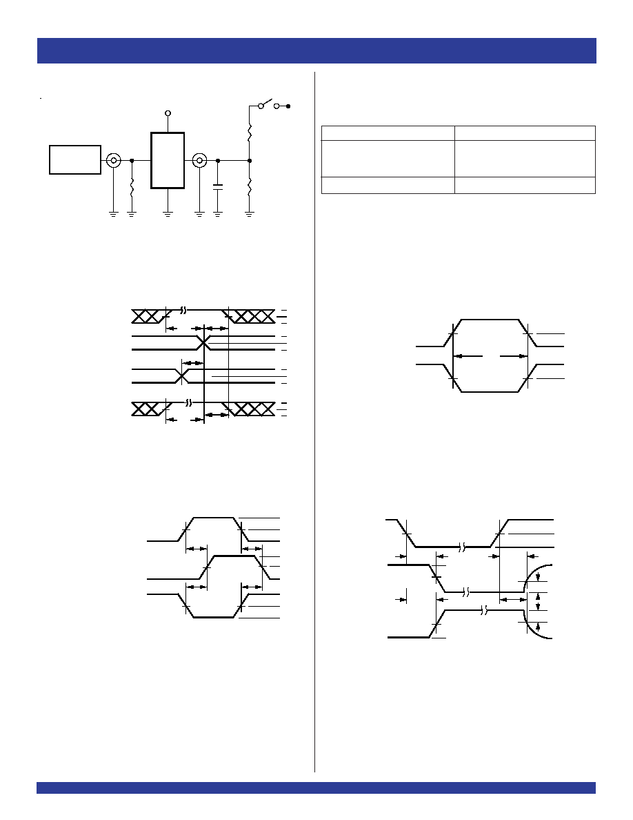
1. See test circuits and waveforms.
2. Minimum limits are guaranteed but not tested on Propagation Delays.
3. This condition guaranteed but not tested.
COMMERCIAL TEMPERATURE RANGE
IDT74FCT863A/B
HIGH-PERFORMANCE CMOS 9-BIT NON-INVERTING TRANSCEIVER
5
Pulse
Generator
R
T
D.U.T
.
V
CC
V
IN
C
L
V
OUT
50pF
500
500
7.0V
3V
1.5V
0V
3V
1.5V
0V
3V
1.5V
0V
3V
1.5V
0V
DATA
INPUT
TIMING
INPUT
ASYNCHRONOUS CONTROL
PRESET
CLEAR
ETC.
SYNCHRONOUS CONTROL
t
SU
t
H
t
REM
t
SU
t
H
HIGH-LOW-HIGH
PULSE
LOW-HIGH-LOW
PULSE
t
W
1.5V
1.5V
SAME PHASE
INPUT TRANSITION
3V
1.5V
0V
1.5V
V
OH
t
PLH
OUTPUT
OPPOSITE PHASE
INPUT TRANSITION
3V
1.5V
0V
t
PLH
t
PHL
t
PHL
V
OL
CONTROL
INPUT
3V
1.5V
0V
3.5V
0V
OUTPUT
NORMALLY
LOW
OUTPUT
NORMALLY
HIGH
SWITCH
CLOSED
SWITCH
OPEN
V
OL
0.3V
0.3V
t
PLZ
t
PZL
t
PZH
t
PHZ
3.5V
0V
1.5V
1.5V
ENABLE
DISABLE
V
OH
PRESET
CLEAR
CLOCK ENABLE
ETC.
Octal link
Octal link
Octal link
Octal link
Octal link
TEST CIRCUITS AND WAVEFORMS
Propagation Delay
Test Circuits for All Outputs
Enable and Disable Times
Set-Up, Hold, and Release Times
Pulse Width
NOTES:
1. Diagram shown for input Control Enable-LOW and input Control Disable-HIGH.
2. Pulse Generator for All Pulses: Rate
1.0MHz; Z
O
50; t
F
2.5ns; t
R
2.5ns.
Test
Switch
Open Drain
Disable Low
Closed
Enable Low
All Other Tests
Open
SWITCH POSITION
DEFINITIONS:
C
L
= Load capacitance: includes jig and probe capacitance.
R
T
= Termination resistance: should be equal to Z
OUT
of the Pulse Generator.

COMMERCIAL TEMPERATURE RANGE
6
IDT74FCT863A/B
HIGH-PERFORMANCE CMOS 9-BIT NON-INVERTING TRANSCEIVER
ORDERING INFORMATION
CORPORATE HEADQUARTERS
for SALES:
for Tech Support:
2975 Stender Way
800-345-7015 or 408-727-6116
logichelp@idt.com
Santa Clara, CA 95054
fax: 408-492-8674
(408) 654-6459
www.idt.com
IDT XX
Temp. Range
XXXX
Device Type
X
Package
SO
863A
863B
Small Outline IC
9-Bit Non-Inverting Transceiver
74
0∞C to +70∞C
FCT