
1
IDT74FCTL2821T
HIGH-SPEED CMOS BUS INTERFACE 10-BIT REGISTER
EXTENDED COMMERCIAL TEMPERATURE RANGE
SEPTEMBER 1999
1999 Integrated Device Technology, Inc.
DSC-5256/-
c
IDT74FCTL2821T
EXTENDED COMMERCIAL TEMPERATURE RANGE
HIGH-SPEED CMOS
BUS INTERFACE
10-BIT REGISTER
DESCRIPTION:
The IDT74FCTL2821T is a 10-bit high-speed CMOS TTL-compatible
buffered register with 3-state outputs, ideal for driving high capacitance
loads such as memory address and data buses. The 2821 device is a 25
resistor output version, useful for driving transmission lines and reducing
system noise. The 2821 series parts can replace the 821 series to reduce
noise in an existing design. All inputs have clamp diodes for undershoot
noise suppression. All outputs have ground bounce suppression. Outputs
will not load an active bus when Vcc is removed from the device.
FUNCTIONAL BLOCK DIAGRAM
OE
CP
D
Q
CP
Di
Yi
25
FEATURES:
-
Pin and function compatible to the Quality QS74FCT Family
-
Extended commercial range of �40�C to +85�C
-
CMOS power levels: <7.5mW static
-
Available in PDIP, SOIC, and QSOP packages
-
Undershoot clamp diodes on all inputs
-
True TTL input and output compatibility
-
Ground bounce controlled outputs
-
Reduced output swing of 0 to 3.5V
-
Built-in 25
series resistor outputs reduce reflection and other
system noise
-
I
OL
= 12mA
2
EXTENDED COMMERCIAL TEMPERATURE RANGE
IDT74FCTL2821T
HIGH-SPEED CMOS BUS INTERFACE 10-BIT REGISTER
PDIP/ SOIC/ QSOP
TOP VIEW
ABSOLUTE MAXIMUM RATINGS
(1)
Symbol
Description
Max.
Unit
V
TERM(2)
Terminal Voltage with Respect to GND
� 0.5 to +7
V
V
TERM(3)
Terminal Voltage with Respect to GND
� 0.5 to +7
V
T
STG
Storage Temperature
� 65 to +150
�C
I
OUT
DC Output Current
120
mA
I
IK
Continuous Clamp Current,
� 20
mA
I
OK
V
I
< 0 or V
O
< 0
� 50
mA
FCTL
NOTES:
1. Stresses greater than those listed under ABSOLUTE MAXIMUM
RATINGS may cause permanent damage to the device. This is a
stress rating only and functional operation of the device at these or
any other conditions above those indicated in the operational sections
of this specification is not implied. Exposure to absolute maximum
rating conditions for extended periods may affect reliability.
2. V
CC
terminals.
3. All terminals except V
CC
.
CAPACITANCE (T
A
= +25
O
C, f = 1.0MHz)
Symbol
Parameter
(1)
Conditions
Typ.
Max.
Unit
C
IN
Input Capacitance
V
IN
= 0V
6
10
pF
C
OUT
Output Capacitance
V
OUT
= 0V
8
12
pF
FCTL
NOTE:
1. This parameter is measured at characterization but not tested.
2
3
1
V
CC
20
19
18
D
4
D
5
D
3
D
7
D
6
D
1
D
2
D
8
15
16
9
10
23
22
24
21
17
5
6
Y
2
Y
4
Y
3
Y
6
Y
5
Y
1
Y
7
Y
8
7
4
P24-1
SO24-2
SO24-8
8
13
14
11
12
G ND
O E
CP
D
0
D
9
Y
9
Y
0
Di
CP
OE
D
Q
Yi
CP
10
10
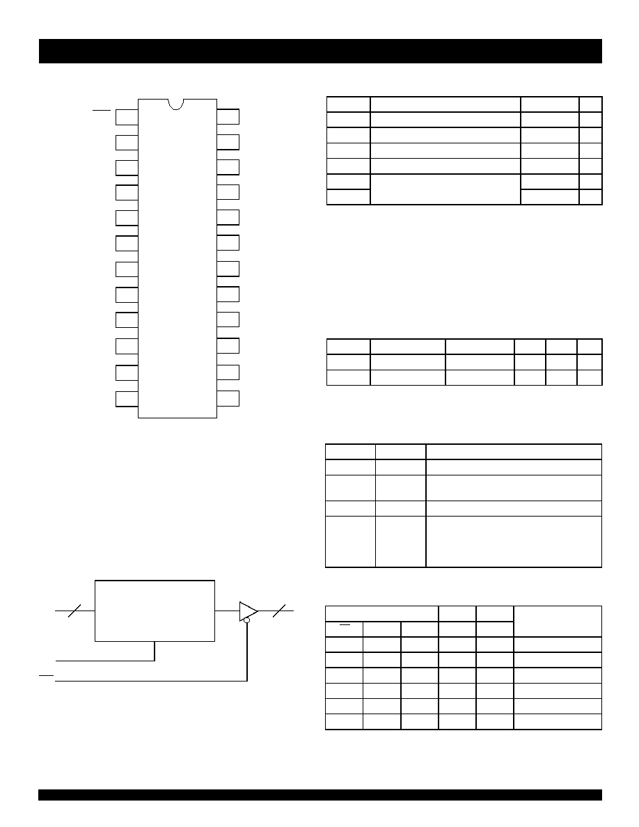
PIN CONFIGURATION
LOGIC SYMBOL
PIN DESCRIPTION
Name
I/O
Description
Di
I
The D flip-flop data inputs.
CP
I
Clock Pulse for the Register; enters data into
the register on the LOW-to-HIGH transition.
Yi
O
The register three-state outputs.
OE
I
Output Control. When the
OE input is HIGH, the
Y
I
outputs are in the high impedance state.
When the
OE input is LOW, the TRUE register
data is present at the Y
I
outputs.
FUNCTION TABLE
(1)
Inputs
Int.
O/P
OE
Di
CP
Qi
Yi
Function
H
L
L
Hi-Z
High Z
H
H
H
Hi-Z
High Z
H
L
L
Hi-Z
Load
H
H
H
Hi-Z
Load
L
L
L
L
Load
L
H
H
H
Load
NOTE:
1. H = HIGH
L = LOW
= LOW-to-HIGH Transition
Z = High-Impedance
3
IDT74FCTL2821T
HIGH-SPEED CMOS BUS INTERFACE 10-BIT REGISTER
EXTENDED COMMERCIAL TEMPERATURE RANGE
DC ELECTRICAL CHARACTERISTICS OVER OPERATING RANGE
Following Conditions Apply Unless Otherwise Specified:
Extended Commercial: T
A
= -40�C to +85�C, V
CC
= 5.0V � 5%
Symbol
Parameter
Test Conditions
Min.
Typ.
(1)
Max.
Unit
V
IH
Input HIGH Level
Guaranteed Logic HIGH Level
2
--
--
V
V
IL
Input LOW Level
Guaranteed Logic LOW Level
--
--
0.8
V
V
T
Input Hysteresis
V
TLH
- V
THL
for all inputs
--
0.2
--
V
I
IH
Input HIGH Current
V
CC
= Max.
0
V
IN
< Vcc
--
--
5
� A
I
IL
Input LOW Current
I
OZ
Off-State Output Current (Hi-Z)
V
CC
= Max.
0
V
IN
Vcc
--
--
5
� A
I
OR
Current Drive
V
CC
= Min., V
OUT
= 2.0V
(2)
50
--
--
mA
V
IC
Input Clamp Voltage
V
CC
= Min., I
IN
= �18mA, T
A
= 25
�
C
--
�0.7
�1.2
V
V
OH
Output HIGH Voltage
V
CC
= Min.
I
OH
= -24mA
2.4
--
--
V
V
OL
Output LOW Voltage - 25
V
CC
= Min.
I
OL
= 12mA
--
--
0.5
V
R
OUT
Output Resistance - 25
V
CC
= Min.
I
OL
= 12mA
20
28
40
NOTES:
1. Typical values are at V
CC
= 5.0V, T
A
= 25�C.
2. Not more than one output should be shorted at one time. Duration of the short circuit test should not exceed one second.
POWER SUPPLY CHARACTERISTICS
Following Conditions Apply Unless Otherwise Specified:
Extended Commercial:
T
A
= -40�C to +85�C, V
CC
= 5.0V � 5%
Symbol
Parameter
Test Conditions
(1)
Min.
Max.
Unit
I
CC
Quiescent Power Supply Current
V
CC
= Max.
freq = 0
0V
V
IN
0.2V or
Vcc-0.2V
V
IN
Vcc
--
1.5
mA
I
CC
Supply Current per Input TTL Inputs HIGH
V
CC
= Max.
V
IN
= 3.4V
(2)
freq = 0
--
2
mA
I
CCD
Supply Current per Input per MHz
V
CC
= Max.
Outputs Open and Enabled
One Bit Toggling
50% Duty Cycle
Other inputs at GND or Vcc
(3,4)
--
0.25
mA/MHz
FCTL
NOTES:
1. For conditions shown as Min. or Max., use the appropriate values specified under DC Electrical Characteristics.
2. Per TLL driven input (V
IN
= 3.4V).
3. For flip-flops, Q
CCD
is measured by switching one of the data input pins so that the output changes every clock cycle. This is a measurement of
device power consumption only and does not include power to drive load capacitance or tester capacitance.
4. I
C
= I
QUIESCENT
+ I
INPUTS
+ I
DYNAMIC
I
C
= I
CC
+
I
CC
D
H
N
T
+ I
CCD
(f
CP
/2 + f
i
N
i
)
I
CC
= Quiescent Current
I
CC
= Power Supply Current for a TTL High Input (V
IN
= 3.4V)
D
H
= Duty Cycle for TTL Inputs High
N
T
= Number of TTL Inputs at D
H
I
CCD
= Dynamic Current Caused by an Output Transition Pair (HLH or LHL)
f
CP
= Clock Frequency for Register Devices (Zero for Non-Register Devices)
f
i
= Input Frequency
N
i
= Number of Inputs at f
i
All currents are in milliamps and all frequencies are in megahertz.

4
EXTENDED COMMERCIAL TEMPERATURE RANGE
IDT74FCTL2821T
HIGH-SPEED CMOS BUS INTERFACE 10-BIT REGISTER
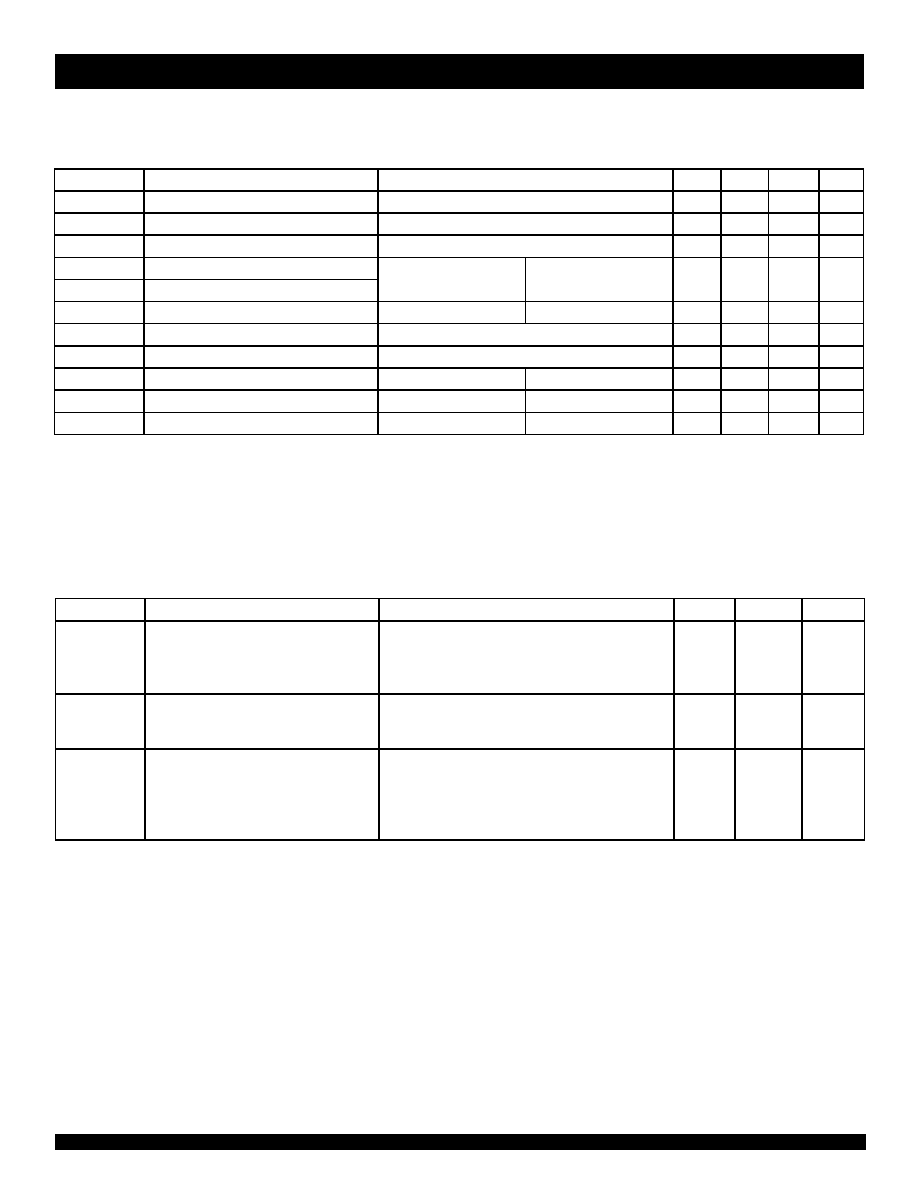
SWITCHING CHARACTERISTICS OVER OPERATING RANGE
(1)
Following Conditions Apply Unless Otherwise Specified:
Extended Commercial: T
A
= -40�C to +85�C, V
CC
= 5.0V � 5%
74FCTL2821AT
74FCTL2821BT
Symbol
Parameter
Min.
Max.
Min.
Max.
Unit
t
PHL
t
PLH
Clock to Y Delay
OE = LOW
--
10
--
7.5
ns
t
PHL
t
PLH
Clock to Y Delay
OE = LOW
(2)
--
20
--
15
ns
t
SU
Data to CP Setup Time
4
--
3
--
ns
t
H
Data to CP Hold Time
2
--
1.5
--
ns
NOTES:
1. C
LOAD
= 50pF, R
LOAD
= 500
unless otherwise noted.
2. C
LOAD
= 300pF
TIMING REQUIREMENTS OVER OPERATING RANGE
(1)
74FCTL2821AT
74FCTL2821BT
Symbol
Parameter
(2)
Min.
Max.
Min.
Max.
Unit
t
PWH
t
PWL
Clock Pulse Width
HIGH or LOW
7
--
6
--
ns
t
PZH
t
PZL
Output Enable Time
OE to Yi
--
12
--
8
ns
t
PZH
t
PZL
Output Enable Time
(3)
OE to Yi
--
23
--
--
ns
t
PHZ
t
PLZ
Output Disable Time
(4)
OE to Yi
--
7
--
6.5
ns
t
PHZ
t
PLZ
Output Disable Time
OE to Yi
--
9
--
7.5
ns
NOTES:
1. C
LOAD
= 50pF, R
LOAD
= 500
unless otherwise noted.
2. See Test Circuits and Waveforms.
3. C
LOAD
= 300pF
4. C
LOAD
= 5pF

5
IDT74FCTL2821T
HIGH-SPEED CMOS BUS INTERFACE 10-BIT REGISTER
EXTENDED COMMERCIAL TEMPERATURE RANGE
Pulse
Generator
R
T
D.U.T.
V
CC
V
IN
C
L
V
OUT
50pF
500
500
7.0V
3V
1.5V
0V
3V
1.5V
0V
3V
1.5V
0V
3V
1.5V
0V
DATA
IN PU T
TIM IN G
IN PU T
ASYN CH R ON OUS C ON TROL
PRES ET
CLEAR
ETC.
SYNC HRO N OU S CON TRO L
t
SU
t
H
t
REM
t
SU
t
H
HIGH-LOW -HIGH
PULSE
LO W -H IGH -LOW
PULSE
t
W
1.5V
1.5V
SAM E PHASE
IN PU T TR ANSITION
3V
1.5V
0V
1.5V
V
OH
t
PLH
OU TPUT
OPPOSITE P HASE
IN PU T TR ANSITION
3V
1.5V
0V
t
PLH
t
PH L
t
PH L
V
OL
CO NTR OL
IN PU T
3V
1.5V
0V
3.5V
0V
OU TPUT
NO RM A LLY
LO W
OU TPUT
NO RM A LLY
HIGH
SW ITC H
CLOSE D
SW ITC H
OPEN
V
OL
0.3V
0.3V
t
PLZ
t
PZL
t
PZH
t
PHZ
3.5V
0V
1.5V
1.5V
ENAB LE
DISA BLE
V
OH
PRES ET
CLEAR
CLOC K ENABLE
ETC.
O ctal lin k
O ctal lin k
O ctal lin k
O ctal lin k
O ctal lin k
TEST CIRCUITS AND WAVEFORMS
PROPAGATION DELAY
TEST CIRCUITS FOR ALL OUTPUTS
ENABLE AND DISABLE TIMES
SET-UP, HOLD, AND RELEASE TIMES
PULSE WIDTH
NOTES:
1. Diagram shown for input Control Enable-LOW and input Control Disable-
HIGH
2. Pulse Generator for All Pulses: Rate
1.0MHz; t
F
2.5ns; t
R
2.5ns
SWITCH POSITION
Test
Switch
Open Drain
Disable Low
Closed
Enable Low
All Other Tests
Open
FCTL
DEFINITIONS:
C
L
= Load capacitance: includes jig and probe capacitance.
R
T
= Termination resistance: should be equal to Z
OUT
of the Pulse
Generator.