
INDUSTRIAL TEMPERATURE RANGE
IDT74LVC4245A
CMOS OCTAL BUS TRANSCEIVER AND 3.3V TO 5V SHIFTER
1
JULY 2000
INDUSTRIAL TEMPERATURE RANGE
The IDT logo is a registered trademark of Integrated Device Technology, Inc.
© 2000 Integrated Device Technology, Inc.
DSC-4754/1
FEATURES:
∑ 0.5 MICRON CMOS Technology
∑ V
CCA
= 5V ± 0.5V
∑ V
CCB
= 2.7V to 3.6V
∑ CMOS power levels (0.4
µµ
µµ
µ W typ. static)
∑ Rail-to-rail output swing for increased noise margin
∑ All inputs, outputs, and I/O are 5V tolerant
∑ Supports hot insertion
∑ Available in SOIC, SSOP, QSOP, and TSSOP packages
FUNCTIONAL BLOCK DIAGRAM
APPLICATIONS:
∑ 5V and 3.3V mixed voltage systems
∑ Data communication and telecommunication systems
DRIVE FEATURES:
∑ High Output Drivers: ±24mA
∑ Reduced system switching noise
IDT74LVC4245A
DESCRIPTION:
The LVC4245A is manufactured using advanced dual metal CMOS
technology. This octal noninverting bus transceiver contains two separate
supply rails; B port has V
CCB
, which is set at 3.3V, and A port has V
CCA
, which
is set at 5V. This allows for translation from a 3.3V to a 5V environment, and
vice-versa.
This device is ideal for asynchronous communication between two buses
(A and B). The direction control pin (DIR) controls the direction of data flow.
The output enable pin (OE) overrides the direction control and disables both
ports. All inputs are designed with hysteresis for improved noise margin.
The LVC4245A has been designed with a ±24mA output driver. This
driver is capable of driving a moderate to heavy load while maintaining
speed performance.
CMOS OCTAL BUS
TRANSCEIVER AND 3.3V TO 5V
SHIFTER WITH 3-STATE OUT-
PUTS AND 5 VOLT TOLERANT I/O
DIR
A
1
A
2
A
3
A
4
A
5
A
6
A
7
A
8
B
8
B
7
B
6
B
5
B
4
B
3
B
2
B
1
OE
2
3
4
5
6
7
8
9
10
14
15
16
17
18
19
20
21
22
5
V
P
o
r
t
3
.
3
V
P
o
r
t

INDUSTRIAL TEMPERATURE RANGE
2
IDT74LVC4245A
CMOS OCTAL BUS TRANSCEIVER AND 3.3V TO 5V SHIFTER
PIN CONFIGURATION
SOIC/ SSOP/ QSOP/ TSSOP
TOP VIEW
Pin Names
Description
OE
Output Enable Input (Active LOW)
DIR
Direction Control Input
A x
Port A Inputs or 3-State Outputs
B x
Port B Inputs or 3-State Outputs
PIN DESCRIPTION
2
3
1
A
1
20
19
18
B
4
B
3
B
5
B
1
B
2
15
B
7
B
8
16
9
GND
10
A
8
B
6
23
22
24
21
17
DIR
5
6
A
6
7
A
4
A
5
4
A
2
A
3
8
A
7
OE
13
14
11
GND
12
V
CCB
(3.3V)
V
CCB
(3.3V)
GND
(5V) V
CCA
NOTE:
1. H = HIGH Voltage Level
L = LOW Voltage Level
X = Don't Care
Inputs
OE
DIR
Outputs
L
L
Bus B Data to Bus A
L
H
Bus A Data to Bus B
H
X
High Z state
FUNCTION TABLE
(1)
NOTES:
1. As applicable to the device type.
2. For A port only.
3. For B port only.
Symbol Parameter
(1)
Conditions
Typ. Max. Unit
C
IN
Input Capacitance
V
IN
= 0V or V
CCA
5
--
pF
V
CCA
= Open
C
I/O
I/O Port Capacitance
(2)
V
OUT
= V
CCA
or GND
11
--
pF
V
CCA
= 5V
C
I/O
I/O Port Capacitance
(3)
V
IN
= V
CCB
or GND
11
--
pF
V
CCB
= 3.3V
CAPACITANCE
(T
A
= +25∞C, F = 1.0MHz)
ABSOLUTE MAXIMUM RATINGS
FOR V
CCB
OR V
CCB
(1)
Symbol
Description
Max
Unit
V
TERM
Terminal Voltage with Respect to GND
≠0.5 to +6.5
V
T
STG
Storage Temperature
≠65 to +150
∞C
I
OUT
DC Output Current
≠50 to +50
mA
I
IK
Continuous Clamp Current,
≠50
mA
I
OK
V
I
< 0 or V
O
< 0
I
CC
Continuous Current through each
±100
mA
I
SS
V
CC
or GND
NOTE:
1. Stresses greater than those listed under ABSOLUTE MAXIMUM RATINGS may cause
permanent damage to the device. This is a stress rating only and functional operation
of the device at these or any other conditions above those indicated in the operational
sections of this specification is not implied. Exposure to absolute maximum rating
conditions for extended periods may affect reliability.

INDUSTRIAL TEMPERATURE RANGE
IDT74LVC4245A
CMOS OCTAL BUS TRANSCEIVER AND 3.3V TO 5V SHIFTER
3
Symbol
Parameter
Test Conditions
Min.
Typ.
(2)
Max.
Unit
V
IH
Input HIGH Voltage Level
V
CCA
= 4.5V to 5.5V
2
--
--
V
V
IL
Input LOW Voltage Level
V
CCA
= 4.5V to 5.5V
--
--
0.8
V
I
IH
Input Leakage Current
V
CCA
= 5.5V
V
I
= 0 to 5.5V
--
--
±1
µA
I
IL
I
OZH
High Impedance Output Current
V
CCA
= 5.5V
V
O
= 0 to 5.5V
--
--
±5
µA
I
OZL
(3-State Output pins)
V
H
Input Hysteresis
V
CCA
= 5V
--
100
--
mV
I
CCL
Quiescent Power Supply Current
V
CCA
= 5.5V
V
IN
= GND or V
CCA
--
--
80
µA
I
CCH
I
CCZ
I
CC
Quiescent Power Supply Current
One input at 3.4V, other inputs at V
CCA
or GND
--
--
1.5
mA
Variation
V
CCA
= 4.5V to 5.5V
DC ELECTRICAL CHARACTERISTICS OVER OPERATING RANGE (A PORT)
Following Conditions Apply Unless Otherwise Specified:
Operating Condition: T
A
= ≠40∞C to +85∞C, V
CCA
= 5V ± 0.5V
(1)
NOTES:
1. V
CCB
= 2.7V to 3.6V.
2. Typical values are at V
CCA
= 5V, +25∞C ambient.
Symbol
Parameter
Test Conditions
Min.
Typ.
(2)
Max.
Unit
V
IH
Input HIGH Voltage Level
V
CCB
= 2.7V to 3.6V
2
--
--
V
V
IL
Input LOW Voltage Level
V
CCB
= 2.7V to 3.6V
--
--
0.8
V
I
OZH
High Impedance Output Current
V
CCB
= 3.6V
V
O
= 0 to V
CCB
--
--
±5
µA
I
OZL
(3-State Output pins)
V
H
Input Hysteresis
V
CCB
= 3.3V
--
100
--
mV
I
CCL
Quiescent Power Supply Current
V
CCB
= 3.6V
V
IN
= GND or V
CCB
--
--
50
µA
I
CCH
I
CCZ
I
CC
Quiescent Power Supply Current
One input at V
CCB
- 0.6V, other inputs at V
CCB
or GND
--
--
500
µA
Variation
V
CCB
= 2.7V to 3.6V
DC ELECTRICAL CHARACTERISTICS OVER OPERATING RANGE (B PORT)
Following Conditions Apply Unless Otherwise Specified:
Operating Condition: T
A
= ≠40∞C to +85∞C, V
CCB
= 2.7V to 3.6V
(1)
NOTES:
1. V
CCA
= 5V ± 0.5V.
2. Typical values are at V
CCB
= 3.3V, +25∞C ambient.

INDUSTRIAL TEMPERATURE RANGE
4
IDT74LVC4245A
CMOS OCTAL BUS TRANSCEIVER AND 3.3V TO 5V SHIFTER
NOTE:
1. V
IH
and V
IL
must be within the min. or max. range shown in the DC ELECTRICAL CHARACTERISTICS OVER OPERATING RANGE table for the appropriate V
CC
range.
T
A
= ≠ 40∞C to + 85∞C, V
CCB
= 2.7V to 3.6V.
OUTPUT DRIVE CHARACTERISTICS, V
CCA
= 5V ± 0.5V (A PORT)
Symbol
Parameter
Test Conditions
(1)
Min.
Max.
Unit
V
OH
Output HIGH Voltage
V
CCA
= 4.5V
I
OH
= ≠ 0.1mA
4.3
--
V
(B Port to A Port)
V
CCA
= 5.5V
5.3
--
V
CCA
= 4.5V
I
OH
= ≠ 24mA
3.7
--
V
CCA
= 5.5V
4.7
--
V
OL
Output LOW Voltage
V
CCA
= 4.5V
I
OL
= 0.1mA
--
0.2
V
(B Port to A Port)
V
CCA
= 5.5V
--
0.2
V
CCA
= 4.5V
I
OL
= 24mA
--
0.55
V
CCA
= 5.5V
--
0.55
NOTE:
1. V
IH
and V
IL
must be within the min. or max. range shown in the DC ELECTRICAL CHARACTERISTICS OVER OPERATING RANGE table for the appropriate V
CC
range.
T
A
= ≠ 40∞C to + 85∞C, V
CCA
= 5V ± 0.5V.
OUTPUT DRIVE CHARACTERISTICS, V
CCB
= 2.7V TO 3.6V (B PORT)
Symbol
Parameter
Test Conditions
(1)
Min.
Max.
Unit
V
OH
Output HIGH Voltage
V
CCB
= 2.7V to 3.6V
I
OH
= ≠ 0.1mA
V
CC
≠ 0.2
--
V
(A Port to B Port)
V
CCB
= 2.7V
I
OH
= ≠ 12mA
2.2
--
V
CCB
= 3V
2.4
--
V
CCB
= 3V
I
OH
= ≠ 24mA
2
--
V
OL
Output LOW Voltage
V
CCB
= 2.7V to 3.6V
I
OL
= 0.1mA
--
0.2
V
(A Port to B Port)
V
CCB
= 2.7V
I
OL
= 12mA
--
0.4
V
CCB
= 3V
I
OL
= 24mA
--
0.55
OPERATING CHARACTERISTICS, T
A
= 25∞C
V
CCA
= 5V, V
CCB
= 3.3V
Symbol
Parameter
Test Conditions
Typical
Unit
C
PD
Power Dissipation Capacitance per Transceiver Outputs enabled
C
L
= 0pF, f = 10Mhz
39.5
pF
C
PD
Power Dissipation Capacitance per Transceiver Outputs disabled
5

INDUSTRIAL TEMPERATURE RANGE
IDT74LVC4245A
CMOS OCTAL BUS TRANSCEIVER AND 3.3V TO 5V SHIFTER
5
SWITCHING CHARACTERISTICS
(1)
V
CCA
= 5V ± 0.5V
V
CCB
= 2.7V to 3.6V
Symbol
Parameter
Min.
Max.
Unit
t
PLH
Propagation Delay
1
6.3
ns
t
PHL
Ax to Bx
1
6.7
t
PLH
Propagation Delay
1
6.1
ns
t
PHL
Bx to Ax
1
5
t
PZL
Output Enable Time
1
8.8
ns
t
PLZ
OE to Bx
1
9.8
t
PZL
Output Enable Time
1
9
ns
t
PLZ
OE to Ax
1
8.1
t
PLZ
Output Disable Time
1
7.7
ns
t
PHZ
OE to Bx
1
7.8
t
PLZ
Output Disable Time
1
7
ns
t
PHZ
OE to Ax
1
5.8
NOTE:
1. See TEST CIRCUITS AND WAVEFORMS. T
A
= ≠ 40∞C to + 85∞C.

INDUSTRIAL TEMPERATURE RANGE
6
IDT74LVC4245A
CMOS OCTAL BUS TRANSCEIVER AND 3.3V TO 5V SHIFTER
t
PLZ
t
PZH
t
PHZ
0V
V
OL+
0.3V
V
OH
t
PZL
V
OL
V
OH-
0.3V
1.5V
3V
0V
1.5V
Output
Control
V
CC
Output
Waveform 1
S1 at 2 X V
CC
(see Note B)
Output
Waveform 2
S1 at GND
(see Note B)
2 x V
CC
GND
Open
C
L
= 50pF
(see Note A)
From Output
Under Test
S1
500
500
1.5V
V
CC
0V
1.5V
Input
t
W
1.5V
V
CC
0V
1.5V
Input
t
PHL
t
PLH
Output
V
OH
V
OL
50% V
CC
50% V
CC
50% V
CC
50% V
CC
LOAD CIRCUIT AND VOLTAGE WAVEFORMS
PARAMETER MEASUREMENT INFORMATION (A PORT)
Load Circuit
Voltage Waveforms Pulse Duration
Voltage Waveforms Propagation Delay Times
Noninverting Outputs
Voltage Waveforms Enable and Disable Times
Low- and High-Level Enabling
NOTES:
A. C
L
includes probe and jig capacitance.
B. Waveform 1 is for an output with internal conditions such that the output is LOW except when disabled by the output control.
Waveform 2 is for an output with internal conditions such that the output is HIGH except when disabled by the output control.
C. All input pulses are supplied by generators having the following characteristics: PRR
10MHz; Zo = 50; t
F
2.5ns; t
R
2.5ns.
D. The outputs are measured one at a time with one transition per measurement.
TEST CONDITIONS
TEST
S1
t
PLH
/ t
PHL
Open
t
PLZ
/ t
PZL
2 x V
CC
t
PHZ
/ t
PZH
GND

INDUSTRIAL TEMPERATURE RANGE
IDT74LVC4245A
CMOS OCTAL BUS TRANSCEIVER AND 3.3V TO 5V SHIFTER
7
t
PLZ
t
PZH
t
PHZ
0V
V
OL+
0.3V
V
OH
t
PZL
V
OL
V
OH-
0.3V
1.5V
3V
0V
1.5V
Output
Control
3.5V
Output
Waveform 1
S1 at 7V
(see Note B)
Output
Waveform 2
S1 at GND
(see Note B)
7V
GND
Open
C
L
= 50pF
(see Note A)
From Output
Under Test
S1
500
500
1.5V
3V
0V
1.5V
Input
t
W
1.5V
3V
0V
1.5V
Input
t
PHL
t
PLH
Output
V
OH
V
OL
1.5V
1.5V
1.5V
1.5V
Load Circuit
Voltage Waveforms Pulse Duration
Voltage Waveforms Propagation Delay Times
Noninverting Outputs
Voltage Waveforms Enable and Disable Times
Low- and High-Level Enabling
LOAD CIRCUIT AND VOLTAGE WAVEFORMS
PARAMETER MEASUREMENT INFORMATION (B PORT)
NOTES:
A. C
L
includes probe and jig capacitance.
B. Waveform 1 is for an output with internal conditions such that the output is LOW except when disabled by the output control.
Waveform 2 is for an output with internal conditions such that the output is HIGH except when disabled by the output control.
C. All input pulses are supplied by generators having the following characteristics: PRR
10MHz; Zo = 50; t
F
2.5ns; t
R
2.5ns.
D. The outputs are measured one at a time with one transition per measurement.
TEST CONDITIONS
TEST
S1
t
PLH
/ t
PHL
Open
t
PLZ
/ t
PZL
7V
t
PHZ
/ t
PZH
GND
INDUSTRIAL TEMPERATURE RANGE
8
IDT74LVC4245A
CMOS OCTAL BUS TRANSCEIVER AND 3.3V TO 5V SHIFTER
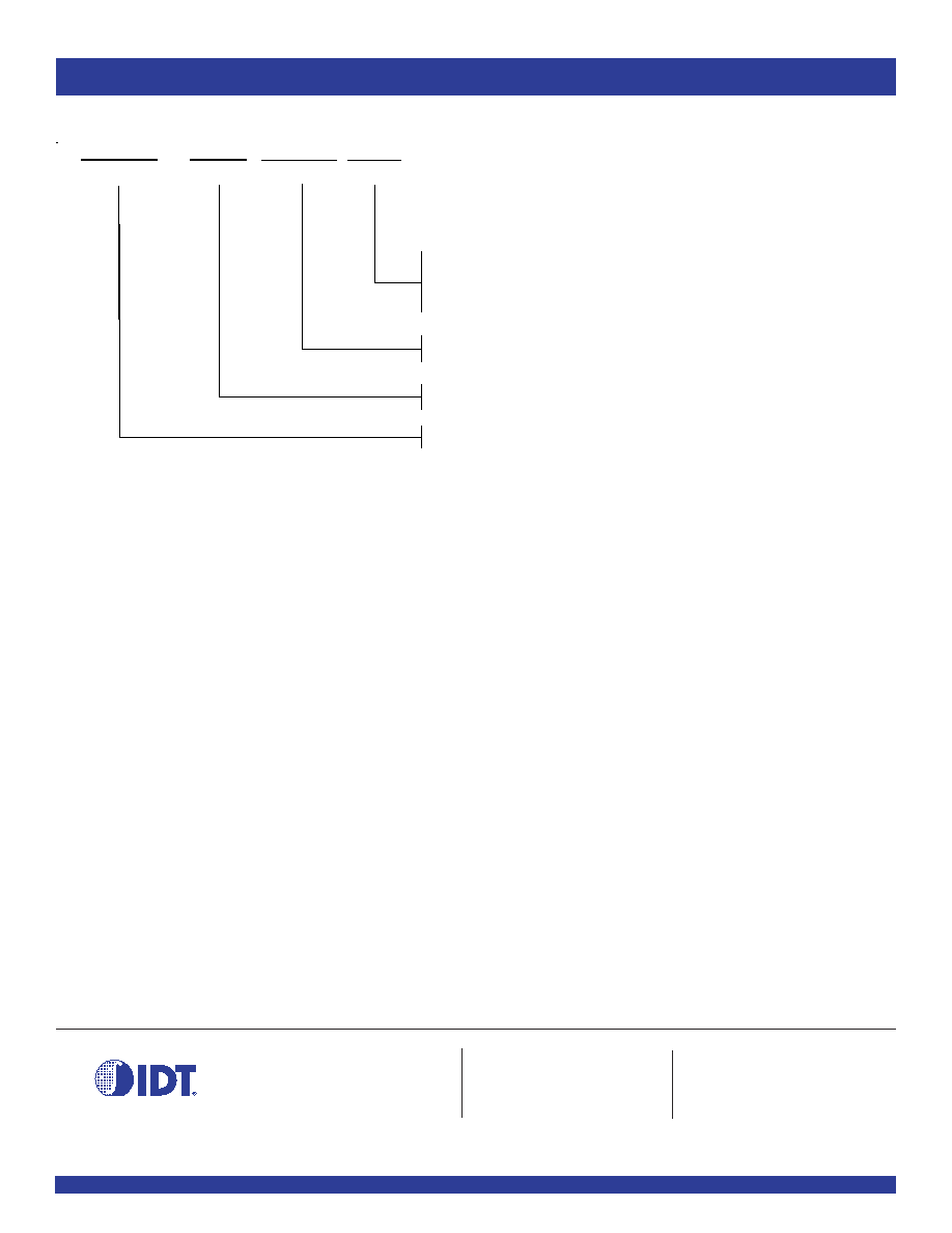
ORDERING INFORMATION
CORPORATE HEADQUARTERS
for SALES:
for Tech Support:
2975 Stender Way
800-345-7015 or 408-727-6116
logichelp@idt.com
Santa Clara, CA 95054
fax: 408-492-8674
(408) 654-6459
www.idt.com
IDT
XX
LVC
XXXX
XX
Package
Device Type
Temp. Range
SO
PY
Q
PG
74
Small Outline IC (gull wing)
Shrink Small Outline Package
Quarter Size Small Outline Package
Thin Shrink Small Outline Package
≠40∞C to +85∞C
X
Bus-Hold
4245A
No Bus-hold
Blank
Octal Bus Transceiver and 3.3V to 5V Shifter with 3-State
Outputs, ±24mA