1
INDUSTRIAL TEMPERATURE RANGE
IDT74SSTV16859
13-BIT TO 26-BIT REGISTERED BUFFER WITH SSTL I/O
MARCH 2002
2002 Integrated Device Technology, Inc.
DSC-5947/4
c
IDT74SSTV16859
PRELIMINARY
INDUSTRIAL TEMPERATURE RANGE
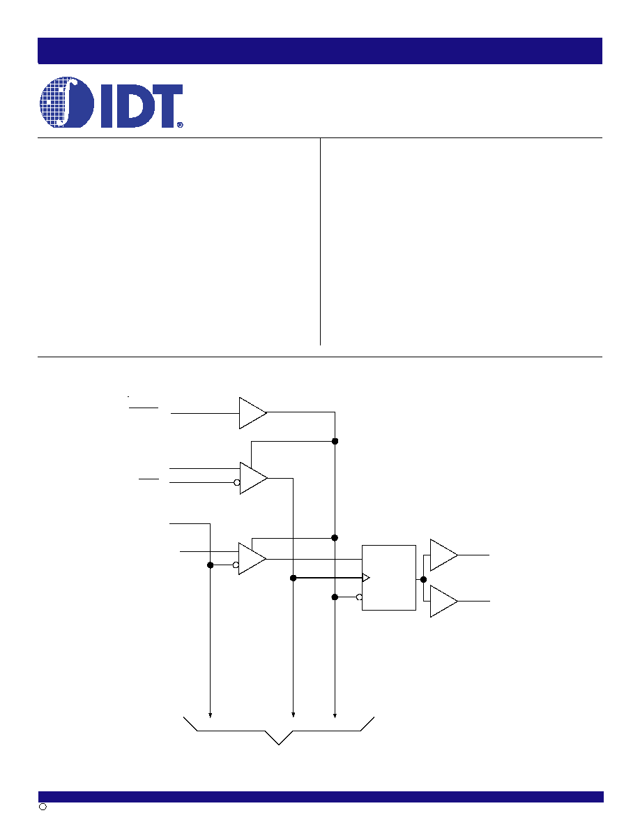
FUNCTIONAL BLOCK DIAGRAM
13-BIT TO 26-BIT REGISTERED
BUFFER WITH SSTL I/O
DESCRIPTION:
The SSTV16859 is a 13-bit to 26-bit registered buffer designed for 2.3V-
2.7V V
DD
and supports low standby operation. All data inputs and outputs
are SSTL_2 level compatible with JEDEC standard for SSTL_2.
RESET is an LVCMOS input since it must operate predictably during the
power-up phase. RESET, which can be operated independent of CLK and
CLK, must be held in the low state during power-up in order to ensure
predictable outputs (low state) before a stable clock has been applied.
RESET, when in the low state, will disable all input receivers, reset all
registers, and force all outputs to a low state, before a stable clock has been
applied. With inputs held low and a stable clock applied, outputs will remain
low during the Low-to-High transition of RESET.
APPLICATIONS:
∑ Ideally suited for DIMM DDR registered applications
51
48
49
45
35
R
1D
C1
16
Q
1A
RESET
CLK
CLK
V
REF
D
1
TO 12 OTH ER CHANNELS
32
Q
1B
FEATURES:
∑ 2.3V to 2.7V Operation
∑ SSTL_2 Class II style data inputs/outputs
∑ Differential CLK input
∑ RESET control compatible with LVCMOS levels
∑ Latch-up performance exceeds 100mA
∑ ESD >2000V per MIL-STD-883, Method 3015; >200V using
machine model (C = 200pF, R = 0)
∑ Available in 56 pin MLF and 64 pin TSSOP packages
The IDT logo is a registered trademark of Integrated Device Technology, Inc.
2
INDUSTRIAL TEMPERATURE RANGE
IDT74SSTV16859
13-BIT TO 26-BIT REGISTERED BUFFER WITH SSTL I/O
PIN CONFIGURATIONS
TSSOP
TOP VIEW
Q
13A
D
1
Q
12A
D
2
G ND
G N D
V
DD Q
V
D D Q
D
3
D
4
D
5
D
6
D
7
Q
6A
Q
7A
V
D DQ
Q
8A
R ESET
D
8
D
9
D
10
D
11
D
12
V
D D
G N D
D
13
64
63
62
61
60
59
58
57
56
55
54
53
52
51
50
49
1
2
3
4
5
6
7
8
9
10
11
12
13
14
15
16
17
18
19
20
21
22
23
24
25
26
27
28
29
30
31
32
48
47
46
45
44
43
42
41
40
39
38
37
36
35
34
33
Q
11A
Q
10A
Q
9A
Q
5A
Q
4A
Q
3A
Q
2A
Q
1A
G ND
Q
13B
V
DD Q
Q
12B
Q
11B
Q
10B
Q
9B
Q
6B
Q
7B
Q
8B
G ND
V
DD Q
Q
5B
Q
4B
Q
3B
Q
2B
Q
1B
G N D
G N D
C LK
C LK
V
D DQ
V
D D
V
R EF
G N D
G N D
V
D DQ
V
D D
G N D
V
D DQ
FUNCTION TABLE
(1)
Input
RESET
CLK
CLK
D
Q Outputs
H
L
L
H
H
H
H
L or H
L or H
X
Qo
(2)
L
X
X
X
L
NOTES:
1. H = HIGH Voltage Level
L = LOW Voltage Level
X = Don't Care
= LOW to HIGH
= HIGH to LOW
2. Qo = Output level before the indicated steady-state conditions were established.
ABSOLUTE MAXIMUM RATINGS
(1)
Symbol
Description
Max.
Unit
V
DD
or V
DDQ
Supply Voltage Range
≠0.5 to 3.6
V
V
I
(2)
Input Voltage Range
≠0.5 to V
DD
+0.5
V
V
O
(3)
Output Voltage Range
≠0.5 to V
DDQ
+0.5
V
I
IK
Input Clamp Current, V
I
< 0
≠50
mA
I
OK
Output Clamp Current,
±50
mA
V
O
< 0 or V
O
> V
DDQ
I
O
Continuous Output Current,
±50
mA
V
O
= 0 to V
DDQ
V
DD
Continuous Current through each
±100
mA
V
DD
, V
DDQ
or GND
T
STG
Storage Temperature Range
≠65 to +150
∞C
NOTES:
1. Stresses greater than those listed under ABSOLUTE MAXIMUM RATINGS may cause
permanent damage to the device. This is a stress rating only and functional operation
of the device at these or any other conditions above those indicated in the operational
sections of this specification is not implied. Exposure to absolute maximum rating
conditions for extended periods may affect reliability.
2. The input and output negative voltage ratings may be exceeded if the ratings of the
I/P and O/P clamp current are observed.
3. The output current will flow if the following conditions are observed:
a) Output in HIGH state
b) V
O
= V
DDQ
MLF
TOP VIEW
Q
1
2
A
V
D
D
Q
Q
8
A
Q
1
1
A
Q
1
0
A
Q
9
A
Q
1
3
A
G
N
D
V
D
D
Q
V
D
D
Q
D
1
1
D
1
2
V
D
D
D
1
3
5
6
4
3
Q
6A
Q
7A
Q
5A
Q
4A
Q
3A
Q
2A
Q
1A
Q
13B
V
DDQ
Q
12B
Q
11B
Q
10B
Q
9B
Q
8B
1
14
D
4
D
5
D
6
D
7
RESET
D
8
D
9
D
10
GND
CLK
CLK
V
DDQ
V
DD
V
REF
42
29
V
D
D
Q
D
1
Q
6
B
Q
7
B
V
D
D
Q
Q
5
B
Q
4
B
Q
3
B
Q
2
B
Q
1
B
D
2
V
D
D
V
D
D
Q
D
3
1
5
2
8
GND
3
INDUSTRIAL TEMPERATURE RANGE
IDT74SSTV16859
13-BIT TO 26-BIT REGISTERED BUFFER WITH SSTL I/O
PIN DESCRIPTION
Pin Names
Description
Q
1
- Q
13
Data Output
GND
Ground
V
DDQ
Output-stage drain power voltage
V
DD
Logic power voltage
RESET
Asynchronous reset input - resets registers and disables data and clock differential input recievers
V
REF
Input reference voltage
CLK
Positive master clock input
CLK
Negative master clock input
D
1
- D
13
Data Input - clocked in on the crossing of the rising edge of CLK and the falling edge of CLK
Center PAD
Ground (MLF package only)
Symbol
Parameter
Test Conditions
Min.
Typ.
Max.
Unit
V
IK
Control Inputs
V
DD
= 2.3V, I
I
=
-18mA
--
--
≠1.2
V
V
OH
V
DD
= 2.3V to 2.7V, I
OH
= -100
µA
V
DD
≠ 0.2
--
--
V
V
DD
= 2.3V, I
OH
= -16mA
1.95
--
--
V
OL
V
DD
= 2.3V to 2.7V, I
OL
= 100
µA
--
--
0.2
V
V
DD
= 2.3V, I
OL
= 16mA
--
--
0.35
I
I
All Inputs
V
DD
= 2.7V,VI = V
DD
or GND
--
--
±5
µA
I
DD
Static Standby
I
O
= 0, V
DD
= 2.7V, RESET = GND
--
--
0.01
mA
Static Operating
I
O
= 0, V
DD
= 2.7V, RESET = V
DD
, V
I
= V
IH (AC)
or V
IL (AC)
--
--
20
Dynamic Operating (Clock Only)
I
O
= 0, V
DD
= 2.7V, RESET = V
DD
, V
I
= V
IH (AC)
or V
IL (AC)
,
--
6
--
µA/Clock
CLK and CLK Switching 50% Duty Cycle.
MHz
I
DDD
Dynamic Operating
I
O
= 0, V
DD
= 2.7V, RESET = V
DD
, V
I
= V
IH (AC)
or V
IL (AC)
,
--
43
--
µA/Clock
(Per Each Data Input)
(1)
CLK and CLK Switching 50% Duty Cycle. One Data Input
MHz/Data
Switching at Half Clock Frequency, 50% Duty Cycle.
Input
r
OH
Output HIGH
V
DD
= 2.3V to 2.7V, I
OH
= -20mA
7
--
20
r
OL
Output LOW
V
DD
= 2.3V to 2.7V, I
OH
= 20mA
7
--
20
r
O(
)
| r
OH
- r
OL
| each separate bit
V
DD
= 2.5V, T
A
= 25∞C, I
OH
= -20mA
--
--
4
Data Inputs
V
DD
= 2.5V, V
I
= V
REF
± 310mV
2
--
3
C
I
CLK and CLK
V
ICR
= 1.25V, V
I (PP)
= 360mV
2
--
3
pF
RESET
V
I
= V
DD
or GND
2
--
3
NOTE:
1. Power dissipation levels will allow operation at DDR333 speeds without excessive die temperature.
DC ELECTRICAL CHARACTERISTICS OVER OPERATING RANGE
Following Conditions Apply Unless Otherwise Specified:
Operating Condition: T
A
= ≠40∞C to +85∞C, V
DD
= 2.5V ±0.2V, V
DDQ
= 2.5V ±0.2V
4
INDUSTRIAL TEMPERATURE RANGE
IDT74SSTV16859
13-BIT TO 26-BIT REGISTERED BUFFER WITH SSTL I/O
OPERATING CHARACTERISTICS, T
A
= 25∫C
(1)
Symbol
Parameter
Min.
Typ.
(1)
Max.
Unit
V
DD
Supply Voltage
V
DDQ
--
2.7
V
V
DDQ
Output Supply Voltage
2.3
2.5
2.7
V
V
REF
Reference Voltage (V
REF
= V
DDQ
/2)
1.15
1.25
1.35
V
V
TT
Termination Voltage
V
REF
≠ 40mV
V
REF
V
REF
+ 40mV
V
V
I
Input Voltage
0
--
V
DD
V
V
IH
AC High-Level Input Voltage
Data Inputs
V
REF
+ 310mV
--
--
V
V
IL
AC Low-Level Input Voltage
Data Inputs
--
--
V
REF
≠ 310mV
V
V
IH
DC High-Level Input Voltage
Data Inputs
V
REF
+ 150mV
--
--
V
V
IL
DC Low-Level Input Voltage
Data Inputs
--
--
V
REF
≠ 150mV
V
V
IH
High-Level Input Voltage
RESET
1.7
--
--
V
V
IL
Low-Level Input Voltage
RESET
--
--
0.7
V
V
ICR
Common-Mode Input Range
CLK, CLK
0.97
--
1.53
V
V
I (PP)
Peak-to-Peak Input Voltage
CLK, CLK
360
--
--
mV
I
OH
High-Level Output Current
--
--
≠ 20
mA
I
OL
Low-Level Output Current
--
--
20
T
A
Operating Free-Air Temperature
≠ 40
--
+85
∞C
NOTE:
1. The RESET input of the device must be held at V
DD
or GND to ensure proper device operation.
SWITCHING CHARACTERISTICS OVER RECOMMENDED FREE-AIR OPERATING
RANGE (UNLESS OTHERWISE NOTED)
V
DD
= 2.5V ± 0.2V
Symbol
Parameter
Min
Max.
Unit
f
MAX
200
--
MHz
t
PD
CLK and CLK to Q
1.1
2.8
ns
t
PHL
RESET to Q
--
5
ns
TIMING REQUIREMENTS OVER RECOMMENDED OPERATING FREE-AIR
TEMPERATURE RANGE
V
DD
= 2.5V ± 0.2V
Symbol
Parameter
Min.
Max.
Unit
CLOCK
Clock Frequency
--
200
MHz
tw
Pulse Duration, CLK, CLK HIGH or LOW
2.5
--
ns
t
ACT
Differential Inputs Active Time
(1)
--
22
ns
t
INACT
Differential Inputs Inactive Time
(2)
--
22
ns
t
SU
Setup Time, Fast Slew Rate
(3, 5)
Data Before CLK
, CLK
0.75
--
ns
Setup Time, Slow Slew Rate
(4, 5)
0.9
--
ns
t
N
Hold Time, Fast Slew Rate
(3,5)
Data Before CLK
, CLK
0.75
--
ns
Hold Time, Slow Slew Rate
(2,5)
0.9
--
ns
NOTES:
1. Data inputs must be low a minimum time of t
ACT
max., after RESET is taken HIGH.
2. Data and clock inputs must be held at valid levels (not floating) a minimum time of t
INACT
max., after RESET is taken LOW.
3. For data signal input slew rate is
1V/ns.
4. For data signal input slew rate is
0.5V/ns and <1V/ns.
5. CLK, CLK signal input slew rates are
1V/ns.
5
INDUSTRIAL TEMPERATURE RANGE
IDT74SSTV16859
13-BIT TO 26-BIT REGISTERED BUFFER WITH SSTL I/O
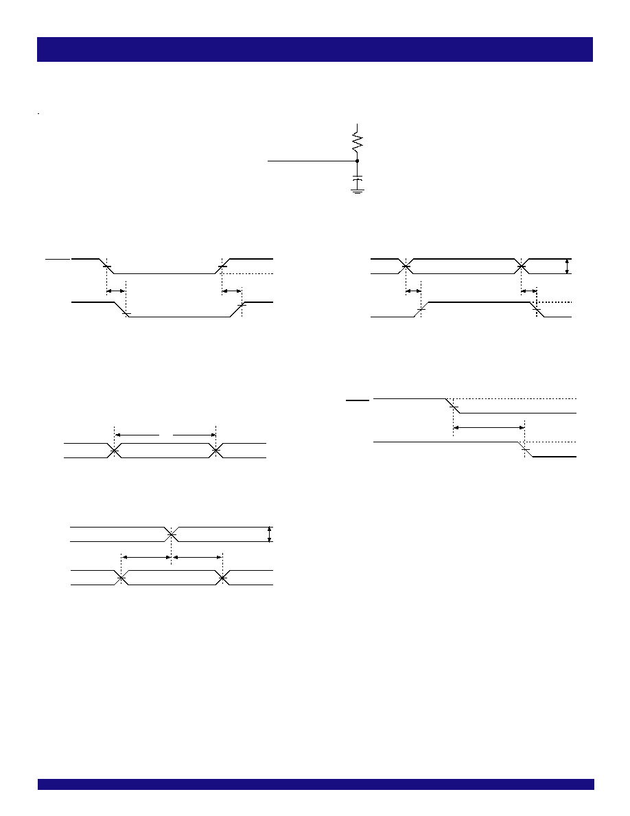
TEST CIRCUITS AND WAVEFORMS (V
DD
= 2.5V ± 0.2V)
Tim ing
Input
V
IC R
V
I(PP )
t
PLH
t
PH L
Output
V
O H
V
O L
V
IC R
V
TT
V
TT
V
O H
V
O L
V
IH
V
IL
t
PH L
V
D D
/2
V
TT
LVCM OS
RESET
Input
Output
V
R E F
V
IH
V
IL
V
RE F
Input
t
W
V
R EF
V
IH
V
IL
V
R E F
Input
V
IC R
V
I(P P)
t
SU
t
N
Tim ing
Input
From Output
Under Test
V
TT
R
L
= 50
C
L
= 30 pF
(see note 1)
Test Point
LVCM OS
RESET
Input
V
D D
/2
V
D D
t
IN AC T
t
AC T
I
DD
V
DD
/2
90%
0V
(see note 2)
10%
Voltage Waveforms - Pulse Duration
NOTES:
1. C
L
includes probe and jig capacitance.
2. I
DD
tested with clock and data inputs held at V
DD
or GND, and I
O
= 0mA.
3. All input pulses are supplied by generators having the following characteristics: PRR
10MHz, Z
O
= 50
, input slew rate = 1 V/ns ±20% (unless otherwise specified).
4. The outputs are measured one at a time with one transition per measurement.
5. V
TT
= V
REF
= V
DDQ
/2
6. V
IH
= V
REF
+ 310mV (AC voltage levels) for differential inputs. V
IH
= V
DD
for LVCMOS input.
7. V
IL
= V
REF
- 310mV (AC voltage levels) for differential inputs. V
IL
= GND for LVCMOS input.
8. t
PLH
and t
PHL
are the same as t
PD
.
Load Circuit
Voltage Waveforms - Setup and Hold Times
Voltage Waveforms - Propagation Delay Times
Voltage Waveforms - Propagation Delay Times
Voltage and Current Waveforms
Inputs Active and Inactive Times