COMMERCIAL TEMPERATURE RANGE
NOVEMBER 1996
©1996 Integrated Device Technology, Inc.
DSC-2066/5
8.03
1
∑ Supports up to 4 PHYs for Multi-PHY connections with 2-
bit address and 8-bit data using UTOPIA 2 protocol.
∑ Provides an 8-bit microprocessor bus interface for
configuration, control and monitoring.
∑ Low power CMOS
∑ 128 pin PQFP Package (14 mm x 20 mm).
DESCRIPTION
The IDT77155 is a member of IDT's SWITCHStAR
TM
family
of products for Asynchronous Transfer Mode (ATM) net-
works.
The IDT77155 is a integrated circuit that provides the
SONET/SDH processing and ATM mapping functions of a
155 Mbps/51 Mbps ATM User Network Interface. Provides full
compliance with SONET/SDH requirements and ATM Forum
Integrated Device Technology, Inc.
NICStAR is a trademark and the IDT logo is a registered trademark of Integrated Device Technology, Inc.
PHY (TC-PMD) USER NETWORK
INTERFACE FOR 155 MBPS ATM
NETWORK APPLICATIONS
ADVANCED
INFORMATION
IDT77155
KEY FEATURES
∑ One chip ATM User Network Interface for 155.52 Mbps/
51.84Mbps operating speed.
∑ Full implementation of the SONET/SDH criteria according
to Bellcore GR-253-CORE and ITU-T G.709, G.783.
∑ Full implementation of the ATM physical layer according
to CCITT I.432 and ATM Forum User Network Interface
Specification.
∑ Full-duplex 155.52 Mbps STS-3c/STM-1 or 51.84 Mbps
STS-1 data with built-in clock/data recovery and clock
synthesis.
∑ Supports 4-cell PHY FIFO buffers for both transmit and
receive directions with parity.
∑ Provides GFC bits insertion and extraction.
∑ UTOPIA Level 1 and Level 2 Interface.
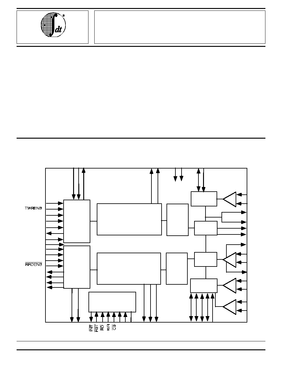
SYSTEM-LEVEL FUNCTIONAL BLOCK DIAGRAM
Encoder
Parallel
to
Serial
Transmit
SONET
Framer
Clk Gen.
Transmit
ATM
Cell
FIFO
Clk Rec.
Serial
to
Parallel
Receive
SONET
Framer
Decoder
Receive
UTOPIA
Cell
FIFO
Encoder
Clk Rec.
RRCLK+
RRCLK-
ALOS+
ALOS-
RXD+
RXD-
RXDO+
RXDO-
RBYP
RCLK
RGFC
RCA
TxADDR[1:0]
TRCLK+
TRCLK-
TXD+
TXD-
TXC+
TXC-
TBYP
RATE0
TCLK
TCP
Transmit
UTOPIA
Cell
FIFO
MPHYEN
APT1
LF≠
LF+
LFO
RALM
RFP
RCP
ATP2
RATE1
TFPO
XOFF
TGFC
TCA
TSOC
TDAT[7:0]
TXPRTY
TFCLK
RSOC
RDAT[7:0]
RXPRTY
RFCLK
TSEN
RxADDR[1:0]
3497 drw 01
Micoprocessor
Interface
D[7:0]
A[7:0]
ALE

8.03
2
IDT77155
ADVANCED INFORMATION
155Mbps ATM PHY (TC-PMD) USER NETWORK INTERFACE
Commercial Temperature Range
GND
GND
IDT77155
TOP
VIEW
PX-128
3497 drw 02
1
2
3
4
5
6
7
8
9
10
11
12
13
14
15
16
17
18
19
20
21
22
23
24
25
26
27
28
29
30
31
32
33
34
35
36
37
38
TBYP
ATP2
AVcc
AGND
AVcc
AGND
AVcc
TRCLK-
TRCLK+
AGND
TXVcc
TXC+
TXC-
TXD+
TXD-
TXGND
Vcc
GND
Vcc
GND
RXDO+
RXDO-
AVcc
RXD-
RXD+
ALOS-
ALOS+
AGND
AVcc
AGND
AVcc
RRCLK-
RRCLK+
AGND
AVcc
AGND
GND
39
40
41
42
43
44
45
46
47
48
49
50
51
52
53
54
55
56
57
58
59
60
61
62
63
64
65
66
67
68
69
70
71
72
73
74
75
76
77
78
79
80
81
82
83
84
85
86
87
88
89
90
91
92
93
94
95
96
97
98
99
100
102
101
128
127
126
125
124
123
122
121
120
119
118
117
116
115
114
113
112
111
110
109
108
107
106
105
VCLK
RATE[0]
RATE[1]
TSOC
TXPRTY
TDAT[7]
TDAT[6]
TDAT[5]
TDAT[4]
TDAT[3]
TDAT[2]
TDAT[1]
TDAT[0]
TCA
TFCLK
RSOC
RXPRTY
Vcc
GND
RDAT[7]
RDAT[6]
RDAT[5]
RDAT[4]
RDAT[3]
RDAT[2]
Vcc
GND
RDAT[1]
RDAT[0]
RCA
RFCLK
TSEN
GND
GND
ALE
A[7]
A[6]
A[5]
A[4]
A[3]
A[2]
A[1]
A[0]
D[7]
D[6]
D[5]
D[4]
Vcc
GND
D[3]
D[2]
D[1]
D[0]
Vcc
GND
GND
GND
ATP1
RBYP
LF+
LF-
LFO
RXADDR[1]
RXADDR[0]
TXADDR[1]
TXADDR[0]
MPHYEN
XOFF
TCP
TGFC
TFPO
TCLK
Vcc
GND
RCLK
RFP
RGFC
RCP
Vcc
GND
RALM
GND
104
103
User Network Interface specifications.
The IDT77155 provides both Transmission Convergence
(TC) and Physical Media Dependent (PMD) sublayer func-
tions of a 155.52 Mbps/51.84 Mbps ATM PHY suitable for
ATM networks. The SONET/SDH interface provides the
SONET/SDH overheads demultiplex and multiplex process-
ing functions. The UTOPIA interface provides standardized
control and communications to other components, such as
Segmentation and Reassembly (SAR) controllers and ATM
switches.
The IDT77155 is fabricated using state-of-the-art CMOS
technology, providing the highest levels of integration, perfor-
mance and reliability, with the low-power consumption char-
acteristics of CMOS.
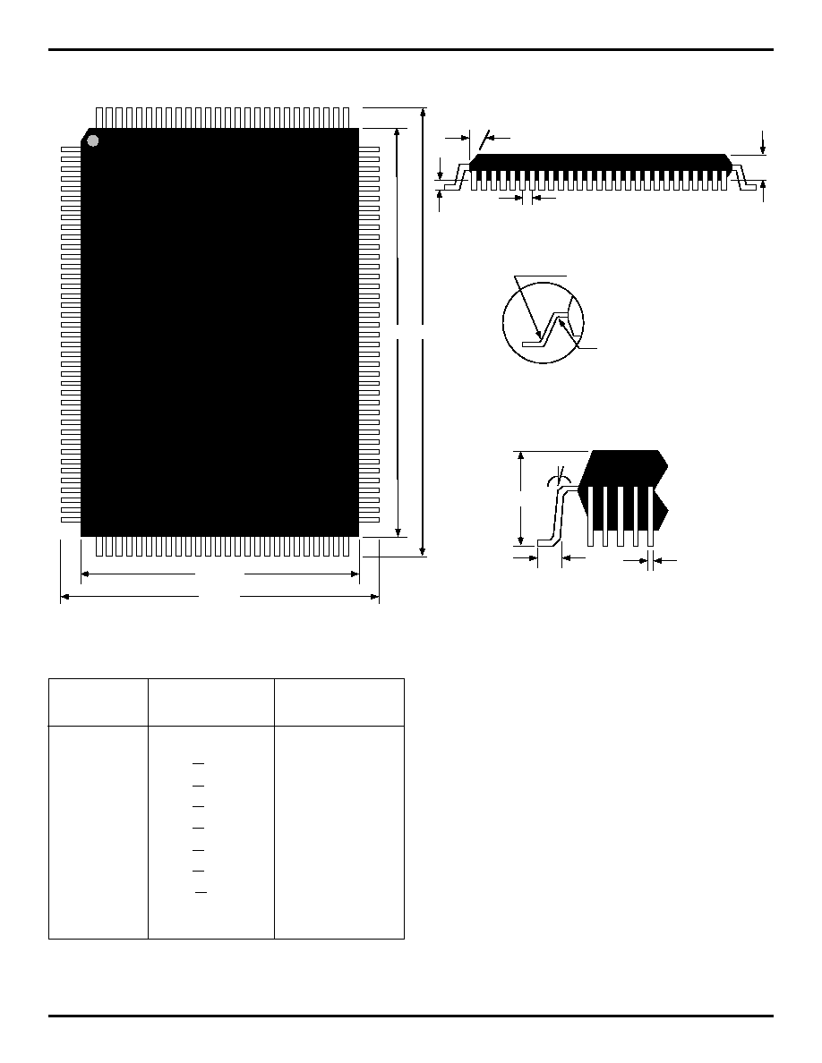
PACKAGE PINOUT
IIDT77155
ADVANCED INFORMATION
155Mbps ATM PHY (TC-PMD) USER NETWORK INTERFACE
Commercial Temperature Range
8.03
3
PACKAGE DIMENSIONS
DIMENSIONS
DIMENSIONS
DIMENSIONS
DIMENSIONS
DIMENSIONS
128-PIN PQFP
DImension
Tolerance
Dimension
Letter
(mm)
(mm)
A
Max.
3.30
A1
+.10
0.35
A2
+.17
2.70
D
+.25
17.20
D1
+.10
14.00
E
+.25
23.20
E1
+.10
20.00
L
+15
0.75
e
Basic
0.50
b
.05
0.22
8'-7"
9'-5"
E1
E
1
128
128-Pin
PQFP
6'-8"
D
5'-10"
D1
2'-0"
b
4
∞
±
4
∞
L
A
A2
e
Draft Angle = 11
∞
≠13
∞
A1
0.20 Rad Typ.
0.20 Rad Typ.
3445 drw 03

8.03
4
IDT77155
ADVANCED INFORMATION
155Mbps ATM PHY (TC-PMD) USER NETWORK INTERFACE
Commercial Temperature Range
Symbol
Name
I/O
Description
A0-A7
Address
I
Address bus to select specific registers in the register set. The address pin A7 has an
integral pull-down resistor.
Pin #: A0/119, A1/120, A2/121, A3/122, A4/123, A5/124, A6/125, A7/126
AGND
Analog Ground
G
These pins should be physically isolated from the other ground pins.
Pin #: 5, 7, 11, 29, 31, 35, 37
ALE
Address Latch
I
Latches the address bus when low, and is transparent when high. It allows interfacing to a
Enable
multiplexed address/data bus. ALE has an integral pull-up resistor.
Pin #: 127
ALOS+
Analog Loss of
I
Differential inputs indicate a loss of receive signal power. When ALOS+/- is asserted, data
ALOS-
Signal
on the RXD+/- inputs is squelched and the receive data/clock recovery PLL switches
to the reference clock. ALOS+/- has an effect only when RBYP is disabled. These inputs
must be dc-coupled.
Pin #: ALOS+ 28, ALOS- 27
ATP1
Test pin
I
Test pin for the transmit clock synthesis logic. When asserted, the TNB output of the clock
synthesis block is reflected on the LFO pin. ATP1 has an integral pull-down resistor.
Pin #: 40
ATP2
Test pin
I
Test pin for the receive clock/data recovery logic. When asserted, the CNB output of the clock
recovery block is reflected on the LF-pin. ATP2 has an integral pull-down resistor.
Pin #: 3
AVcc
Analog Power
P
These power pins should be physically isolated from the other power pins and connected to a
well coupled 5v dc source.
Pin #: 4, 6, 8, 24, 30, 32, 36
CS
Chip Select
I
Active low chip select to access registers.
Pin #: 100
D1-D7
Data
I/O
Bidirectional data bus for register access during register reads and writes.
Pin #: D0/109, D1/110, D2/111, D3/112, D4/115, D5/116, D6/117, D7/118
GND
Ground
G
Core, Ring and Thermal Grounds.
Pin #: 1, 19, 21, 38, 39, 56, 62, 64, 65, 72, 80, 102, 103, 106, 113, 128
INT
Interrupt
O
Open drain interrupt signal which goes low when an interrupt source is active and unmasked
open from within the chip. This signal is cleared by appropriate reads to the interrupt
registers. INT is an open-drain output.
Pin #: 108
LF+
Loop Filter
O
Special pin to output CAP voltage of the receive data/clock recovery logic when ATP2 is
LF-
enabled. Reference clock signal of the receive data/clock recovery logic.
Pin #: LF+/42, LF-/43
LFO
Special
O
Special pin to output CAP voltage of the transmit clock synthesis logic when ATP1 is enabled.
Pin #: 44
MPHYEN
Multi-phy Enable
I
When asserted, the multiphy enable signal converts the UTOPIA interface to be fully
compliant with the UTOPIA level-2 specification. In this mode, the TXADDR[1:0] and
RXADDR[1:0] bits determine the address of the device to be addressed. The default
operation of the chip is in single-phy UTOPIA level-1 mode. MPHYEN pin has an integral pull-
down resistor.
Pin #: 49
RALM
Receive Alarm
O
Output is asserted if line alarm indication signal (LAIS), path alarm indication signal (PAIS),
loss of signal (LOS), loss of frame (LOF), or loss of cell delineation (LOC) is detected in the
receive logic. RALM is updated on the rising edge of RCLK.
Pin #: 63
RATE0
Line Rate
I
RATE inputs select the frame format and line rates for both the transmit and receive functions
RATE1
RATE(1:0)
11
155.52 Mb/s, STS-3c / STM-1
10
51.84 Mb/s, STS-1
0X
Reserved
The RATE inputs have integral pull-up resistors, so the default is STS-3c
Pin #: RATE0/98, RATE1/97
PIN DESCRIPTIONS

IIDT77155
ADVANCED INFORMATION
155Mbps ATM PHY (TC-PMD) USER NETWORK INTERFACE
Commercial Temperature Range
8.03
5
Symbol
Name
I/O
Description
RBYP
Receive Bypass
I
Active high RBYP input disables clock recovery. If enabled, the receive different serial data
RXD+/- is sampled on the rising edged of the receive differential reference clock RRCLK+/-.
If RBYP is disabled, the receive clocks are recovered from RXD+/- bit stream. RBYP has an
integral pull down resistor.
Pin #: 41
RCA/
Receive Cell
O
This signal is asserted to indicate either 0 or a maximum of 4 morebytes are present in the
RXEMPTY
Available
tristate receive FIFO. The indication of the receive FIFO level is programmable, as is the
polarity of this signal. Signal is updated on the rising edge of RFCLK. The RCA signal is
tristated in UTOPIA level-2 mode (MPHYEN asserted) and driven as per the multi-phy
protocol.
Pin #: 69
RCLK
Receive Clock
O
Provides a timing reference, and is a divide-by-8 version of tri-covered clock when RBYP is
disabled or RRCLK+/- when RBYP is enabled.
Pin #: 57
RCP
Receive Cell
O
Receive GFC pulse indicates the start of the four generic flow control bits (GFC) in the
RGFC Pulse output. RCP is coincident with the most significant GFC bits. RCP is updated
on the rising edge of RCLK.
Pin #: 60
RD
Read
I
Active low read signal to read contents of addressed register. The data bus is driven by the
contents of the addresses register when the read signal is asserted along with the chip
select (CS) signal.
Pin #: 105
RDAT0-
Receive Data
O
The receive cell data to the ATM layer from the receive FIFO. This is updated on the rising
RDAT7
edge of RFCLK. RDAT[7:0] is tristated if TSEN is asserted or if MPHYEN is asserted. In
UTOPIA single-phy mode, it is driven if RRDENB is asserted (TSEN also asserted) or
always driven if TSEN is low. In UTOPIA multi-phy mode, RDAT[7:0] is driven following the
level-2 protocol.
Pin #: RDAT0/70, RDAT1/71, RDAT2/74, RDAT3/75, RDAT4/76, RDAT5/77, RDAT6/78,
RDAT7/79
RFCLK
Receive FIFO
I
The receive ATM clock from the ATM layer <= 40 MHz. The start of cell indication, the
Clock
transmit data, and the transmit data parity signals are updated on the rising edge of this
clock. RRDENB is sampled on the rising edge of this clock.
Pin #: 67
RFP
Receive Frame
O
An 8 KHz signal synchronized to RCLK. It is pulse high for one clock every 2430 RCLK
Pulse
cycles for STS-3c or every 810 RCLK cycles for STS-1. It is updated on the rising edge of
RCLK.
Pin #: 58
RGFC
Receive Generic
O
Outputs the extracted generic flow control bits (GFC) in a serial stream. The four GFC bits
Flow Control
are output for each receive cell, and the first of the four bits is coincident with the RCP
output, RGFC is low until cell delineation is achieved. RGFC is updated on the rising edge of
RCLK.
Pin #: 59
RRCLK+
Receive Differential I
Inputs contain a jitter-free 19.44 MHz or a 6.48 MHz reference clock when clock recovery
RRCLK-
Reference Clock
is enabled (RBYP = 0). When RBYP is enabled, RRCLK+/- is nominally a 155.52 MHz or
51.84 MHz 50% duty cycle clock and provides the timing for the internal receive functions.
RXD+/- is sampled on the rising edge of RRCLK+/-
Pin #: RRCLK+/34/ RRCLK-/33
RRDENB
Receive Read
I
Active low signal from ATM signifying that data will be sampled on RDAT[7:0] in the
Enable
following clock cycle. When sampled high, RSOC and RDAT[7:0] are tristated, if TSEN is
enabled. RRDENB must operate with RFCLK at high rate to prevent receive FIFO overflow
and loss of receive data.
Pin #: 68
PIN DESCRIPTIONS (CONTINUED)

8.03
6
IDT77155
ADVANCED INFORMATION
155Mbps ATM PHY (TC-PMD) USER NETWORK INTERFACE
Commercial Temperature Range
Symbol
Name
I/O
Description
RSOC
Receive Start
O
Indication to the ATM layer. This is asserted during the first byte of each tristate cell and is
of Cell
updated on the rising edge of RFCLK. RSOC is tristated if TSEN is asserted or if MPHYEN is
asserted. In UTOPIA single-phy mode, it is driven if RRDENB is asserted (TSEN also
asserted) or always driven if TSEN is low. In UTOPIA multi-phy mode, RSOC is driven
following the level-2 protocol.
Pin #: 83
RST
Reset
I
Active low asynchronous reset from the system. RST has integral pull-up resistor. RST need
not be asserted to reset the chip.
Pin #: 101
RXADDR[0]
Receive Address
I
Receive address indicates the ID of the device which should respond to the receive bus
RXADDR[1]
signals in UTOPIA level-2 multi-phy mode (when MPHYEN is asserted). It indicates the
device which should drive the receive cell to ATM device. The device ID may be programmed
in a receive ID register. The device ID register contain a default address of 0. RXADDR[1:0]
is sampled on the rising edge of RFCLK. RXADDR[1:0] inputs have integral pull-up resistors.
RXADDR[1:0] inputs are ignored when MPHYEN is not asserted.
Pin #: RXADDR0/46, RXADDR1/45
RXD+
Receive
I
NRZ encoded receive differential data inputs which contain STS-3c or STS-1 data, and
RXD-
Differential
sampled on the rising edge of RRCLK+/- if RBYP asserted, else the receive clock are
Data Inputs
recovered from the data stream.
Pin #: RXD+/26, RXD-/25
RXDO+
Receive
O
Sliced versions of the RXD+/- inputs, to allow decision feedback equalization (DFE) to
RXDO-
Differential
correct baseline wander. These outputs could be programmed to be pure PECL. Defaults is a
Data Outputs
rail-to-rail swing.
Pin #: RXDO+/22, RXDO-/25
RXPRTY
Receive Parity
O
Indicates the parity of the RDAT[7:0] bus. Odd or even parity may be selected. Tristate
RXPRTY is enabled on the rising edge of RFCLK, RXPRTY is tristate if TSEN is asserted or
if MPHYEN is asserted. In UTOPIA single-phy mode, it is driven if RRDENB is asserted
(TSEN also asserted) or always driven if TSEN is low. In UTOPIA multi-phy mode, RXPRTY
is driven following the level-2 protocol.
Pin #: 82
TBYP
Transmit Bypass
I
Active high transmit bypass input disables clock generator. If enabled, the clock inputs
TRCLK+/- become the transmit line lock at 155.52 MHz or 51.84 MHz. If disabled, the
transmit clock is synthesized from a 19.44 MHz or 6.48 MHz reference clock on
TRCLK+/-. TBYP has an integral pull down resistor.
Pin #: 2
TCA/
Transmit Cell
O
Signal indicates the availability of a complete cell space in the transmit FIFO. This signal
TXFULL
Available
when asserted indicates a maximum of 4 more transmit data writes will be accepted or that
the transmit FIFO is full and no more writes will be accepted. The indication of the transmit
FIFO level is programmable, as is the polarity of this signal. The FIFO depth at which the
TCA signal indicates the unavailability of data space in the FIFO may be set to one, two,
three, or four cells. TCA is updated on the rising edge of TFCLK.
Pin #: 86
TCLK
Transmit Clock
O
The transmit byte clock provides a timing reference, and is a divide-by-8 version of the
synthesized clock when TBYP is disabled or TRCLK+/- when TBYP is enabled.
Pin #: 54
TCP
Transmit Cell
O
Transmit GFC cell pulse indicates the expected place of the transmit GFC bits. TCP is
Pulse
updated on the rising edge of TCLK.
Pin #: 51
TDAT[0]-
Transmit Cell
I
The transmit cell data from the ATM layer sampled on the rising edge of TFCLK. It carries
TDAT[7]
Data
the 53 cell bytes. It is considered valid only when the TWRENB signal is asserted.
Pin #: TDAT0/87, TDAT1/88, TDAT2/89, TDAT3/90. TDAT4/91, TDAT5/92, TDAT6/93.
TDAT7/94
TFCLK
Transmit FIFO
I
The transmit ATM clock from the ATM layer <= 40 MHz. The start of cell indication, the
Clock
transmit data, the transmit data parity, and the enable signals are sampled on the rising edge
of this clock.
Pin #: 84
PIN DESCRIPTIONS (CONTINUED)

IIDT77155
ADVANCED INFORMATION
155Mbps ATM PHY (TC-PMD) USER NETWORK INTERFACE
Commercial Temperature Range
8.03
7
Symbol
Name
I/O
Description
TFPO
Transmit Framing
O
Transmit frame pulse is an 8 KHz signal synchronized to TCLK. It is pulsed high for one
Position Output
clock every 2430 TCLK cycles for STS-3c or every 810 TCLK cycles for STS-1. It is updated
on the rising edge of TCLK.
Pin #: 53
TGFC
Transmit Generic
I
Input provides the ability to insert GFC values downstream of the transmit FIFO. The four
Flow Control
TCLK periods following TCP output pulse should contain the four GFC bits to be inserted.
The GFC enable bits in a configuration register enable the insertion of each bit. By default,
the GFC values contain the header information of the default idle/unassigned cell header
register. The inserted GFC bits are input into the next immediate cell to be transmitted. TGFC
bits are sampled on the rising edge of TCLK.
Pin #: 52
TRCLK+
Transmit
I
Differential input contain a jitter-free 19.44 MHz or a 6.48 MHz reference clock when clock
TRCLK-
Reference Clock
synthesis is enabled (TBYP = 0). When TBYP is enabled, TRCLK+/- is nominally a 155.52
MHz or 51.84 MHz 50% duty cycle clock and provides the timing for the internal transmit
functions. It may be left unconnected if loop timing is enabled.
Pin #: TRCLK+/10, TRCLK-/9
TSEN
Transmit Enable
I
The tristate enable signal tristates RSOC, RDAT[7:0], and RXPRTY signals. When asserted,
RSOC, RDAT[7:0], and RXPRTY are driven only when RRDENB is asserted. When TSEN is
low, the signals RSOC, RDAT[7:0], and RXPRTY, are always asserted in single-phy UTOPIA
level-1 mode. TSEN has an integral pull-down resistor.
Pin #: 66
TSOC
Transmit Start of
I
The transmit start of cell indication from ATM layer. This should be asserted during the first
Cell
byte of each cell and is sampled on the rising edge of TFCLK. An interrupt is generated while
TSOC is asserted at any byte other than the first byte of the transmit 53 byte cell.
Pin #: 96
TWRENB
Transmit Write
I
Active low transmit enable signal used to initiate writes to the transmit FIFO from the ATM
Enable
device. When asserted low, the byte on TDAT[7:0] is written to the transmit FIFO. A complete
53 byte cell must be written to the FIFO before the cell is inserted into the SPE of the transmit
frame. Idle/unassigned cells are inserted until a complete cell is available for transmission.
Pin #: 85
TXADDR[0]
Transmit Address
I
Indicates the ID of the device which should respond to the transmit bus signals in
TXADDR[1]
transmit bus signals in UTOPIA level-2 multi-phy mode (when MPHYEN is asserted). It
indicates the device which should accept the transmit cell from ATM device. The device ID
may be programmed in a transmit ID register. The device ID register contain a default
address of 0. TXADDR[1:0] is sampled on the rising edge of TFCLK. TXADDR[1:0] inputs
have integral pull-up resistors. TXADDR[1:0] inputs are ignored when MPHYEN is not
asserted.
Pin #: TXADDR0/48, TXADDR1/47
TXC+
Transmit Clock
O
Transmit differential line negative output clock is a buffered version of the input differential
TXC-
clock. These outputs could be programmed to be pure PECL. Default is a rail-to-rail swing, If
these outputs are not programmed to be PECL, then the outputs are squelched in the STS-3c
mode.
Pin #: TSC+/13, TXC-/14
TXD+
Transmit Data
O
NRZ encoded transmit differential data outputs which contain STS-3c or STS-1 data, and
TXD-
updated on the falling edge of TXC+/-. These outputs could be programmed to be pure PECL.
Default is a rail-to-rail swing.
Pin #: TXD+/15, TXD-/16
TXPRTY
Transmit Parity
I
Indicates the parity of the TDAT[7:0] bus. Odd or even parity may be selected. TXPRTY is
sampled on the rising edge of TFCLK and considered valid only when TWRENB is asserted.
TXPRTY has an integral pull-down resistor. A maskable parity error is generated if an error is
detected, but the cells with parity errors are not filtered.
Pin #: 95
TXVcc
Power
P
Power pin for TXC+/- and TXD+/- outputs. Should be physically isolated from the other power
analog pins and connected to a well coupled 5v dc source.
Pin #: 12
PIN DESCRIPTIONS (CONTINUED)

8.03
8
IDT77155
ADVANCED INFORMATION
155Mbps ATM PHY (TC-PMD) USER NETWORK INTERFACE
Commercial Temperature Range
ABSOLUTE MAXIMUM RATINGS
(1)
Symbol
Rating
Commercial
Unit
V
TERM
Terminal Voltage
≠0.5 to +7.0
V
with respect to DVGND
T
A
Operating
0 to +70
∞
C
Temperature
T
BIAS
Temperature Under
≠55 to +125
∞
C
Bias
T
STG
Storage
≠55 to +125
∞
C
Temperature
I
OUT
DC Output Current
50
mA
NOTE:
3139 tbl 02
1. Stresses greater than those listed under ABSOLUTE MAXIMUM RAT-
INGS may cause permanent damage to the device. This is a stress rating
only and functional operation of the device at these or any other conditions
above those indicated in the operational sections of this specification is not
implied. Exposure to absolute maximum rating conditions for extended
periods may affect reliabilty.
Symbol
Parameter
Conditions
Max.
Unit
C
IN
(1)
Input
VIN = 0V
10
pF
Capacitance
C
OUT
(1)
Output
VOUT = 0V
10
pF
Capacitance
CAPACITANCE (TA = +25
∞
C)
NOTE:
3139 tbl 05
1. Characterized values, not currently tested.
Notes
1. All inputs operate at TTL levels except the PECL inputs.
2. RDAT[7:0], RXPRTY, RCP, RGFC, RSOC, TCA, TCLK, RCLK, TCP outputs have an 8 ma drive capability, while all other digital outputs have 4 ms drive.
3. All analog power/ground pins should be isolated from the digital power/ground pins, preferably with separate power supplies. It is recommanded to have
separate ground planes on the board also.
Symbol
Name
I/O
Description
TXGND
Ground
G
Ground pin for TXC+/- and TXD+/- outputs. Should be physically isolated from the other
ground analog pins.
Pin #: 17
Vcc
Power
P
Core and pad ring power connected to a decoupled 5V dc
Pin #: 18, 20, 55, 61, 73, 81, 107, 114
VCLK
Vector Clock
I
VCLK is used as a test mode input to the chip. It should be asserted only when testing the
chip on a tester. It shortens the count values for most receive error counters to enable the
testing to be done in a reasonable amount of time. VCLK has an intergral pull-down registor.
Pin #: 99
WR
Write
I
Active low write signal to update registers. The data bus contents are latched into the
addressed register on the rising edge of the write signal when the chip select (CS) is
asserted.
Pin #: 104
XOFF
Transmit Off
I
Transmit off signal prevents the insertion of cells from the transmit FIFO into the transmit
frames. If asserted, idle/unassigned cells only are transmitted irrespective of the state of the
transmit FIFO. XOFF is an asynchronous signal and has an integral pull-down registor.
Pin #: 50
PIN DESCRIPTIONS (CONTINUED)

IIDT77155
ADVANCED INFORMATION
155Mbps ATM PHY (TC-PMD) USER NETWORK INTERFACE
Commercial Temperature Range
8.03
9
Desired
Desired
Denominator
Window
BIP
Calculated
Calculated
BER
detectiion
multiple
Length
Threshold
BER
detectiopn
trigger
time
trigger
time
1e-3
0.008s
0
64
19
0.988e-3
0.008s
1e-4
0.013s
0
104
2
1.040e-4
0.013s
1e-5
0.100s
20
38
4
0.991e-5
0.0998s
1e-6
1.000s
989
8
19
0.998e-6
0.990s
1e-7
10.00s
7849
10
15
0.994e-7
9.810s
1e-8
83.00s
41615
16
7
0.875e-8
83.23s
1e-9
667.0s
52313
102
1
0.994e-9
666.99s
TABLE 1. B2 BER DETECTION CONFIGURATION TABLE
DC ELECTRICAL CHARACTERISTICS
Symbol
Parameter
Min.
Typ.
Max.
Unit
V
CC
Digital Supply Voltage
4.5
5.0
5.5
V
GND
Digital Ground Voltage
0
0
0
V
V
ILp
PECL Input Low Voltage
Vcc-1.8V
--
Vcc-1.6V
V
V
IHp
PECL Input High Voltage
Vcc-1.0V
--
Vcc-0.8V
V
V
OLp
PECL Output Low Voltage
Vcc-1.8V
--
Vcc-1.6V
V
V
OHp
PECL Outut High Voltage
Vcc-1.0V
--
Vcc-0.8V
V
V
IL
TTL Input Low Voltage
--
--
0.8
V
V
IH
TTL Input High Voltage
2.0
--
--
V
V
OL
TTL Output Low Voltage
--
--
0.4
V
V
OH
TTL Output High Voltage
2.4
--
--
V
AV
CC
Analog Supply Voltage
4.5
5.0
5.5
V
AGND
Analog Ground Voltage
0
0
0
V
I
DD1
Power Supply Current
--
--
85 (155.52Mbps) mA
55 (51.84Mbps)
I
DD2
Average Standby Current
--
--
100
µ
A

8.03
10
IDT77155
ADVANCED INFORMATION
155Mbps ATM PHY (TC-PMD) USER NETWORK INTERFACE
Commercial Temperature Range
FUNCTIONAL DESCRIPTION
CLOCK RECOVERY
The clock recovery Block recovers the clock from the
receiving serial data stream. This block can be selected to
utilize reference clocks at 6.48 MHz or 19.44 MHz. This unit
provides a status bit to indicate whether it is locked to data or
the reference clock. The clock recovery unit also provides a
loss of signal (LOS) input and a diagnostic loopback.
The PLL originally locks to the reference clock. The PPL will
lock to the data when the frequency of the recovered clock is
within 244 ppm of the reference clock. Once in data lock, the
PLL switches to the reference clock if there is no data
transition for an 80 bit period or the recovered clock drifts for
over 244 ppm of the reference clock. The transmit clock could
be derived from the recovered clock (loop timing) by configu-
ration.
SERIAL TO PARALLEL
This block performs the serial to parallel conversion of
incoming bit serial data into byte serial data.
RECEIVE SONET FRAMER
The Receive SONET Framer performs frame synchroniza-
tion, descrambling, pointer interpretation, SONET section,
line, and path overhead processing, alarm and performance
monitoring functions.
The framer determines the out-of-frame/in-frame status for
the STS-3c/STS-1 data by checking the framing pattern (A1,
A2). Out-of-frame is declared when four consecutive frames
with errored framing patterns are received. While out-of-
frame, the framer searches for the correct framing pattern, in-
frame is declared upon detecting two consecutive error-free
framing patterns.
The Loss Of Frame (LOF) status is determined by monitor-
ing the out-of-frame/in-frame conditions. This block provides
the 3 ms out-of-frame timer and in-frame timer. The in-frame
timer accumulates when the out-of-frame is absent; it stops
accumulating and is reset to zero when the out-of-frame is
present. The out-of-frame timer accumulates when the out-of-
frame is present; it stops accumulating when the out-of-frame
is terminated. For the intermittent out-of-frame conditions, it is
only reset to zero when the out-of-frame is absent continu-
ously for 3 ms (i.e., the in-frame timer reaches 3 ms).
The LOF is declared when the accumulated out-of-frame
timer reaches 3 ms. Once detected, the LOF defect is termi-
nated when the in-frame timer reaches 3 ms.
The Loss Of Signal (LOS) Block checks the incoming
scrambled data availability. LOS is declared when 20 + 3
µ
s
of all-zero pattern is detected. Loss of signal is cleared when
two consecutive valid framing patterns is detected, and during
the intervening time (one frame), no all-zero pattern qualifying
as LOS defect exits.
The incoming data stream is descrambled. The scrambling
polynomial is 1 + x
6
+ X
7
and the sequence length is 127. The
framing bytes (A1, A2) and the identity bytes (C1) are not
descrambled. The descrambling function can be disable by a
register control bit.
The B1 BER is monitored by the incoming section BIP-8
error detection code (B1). The BIP-8 code is calculated over
all bits of the complete STS-3c or STS-1 frame before
descrambling by bit interleaved parity calculation using even
parity. And obtains errors by comparing the calculated BIP-8
code with the BIP-8 code extracted from the B1 byte of the next
incoming frame. Up to 64,000 (8 x 8000) bit errors can be
detected for one second.
One 16-bit saturating counter is provided to accumulate
these BIP errors. This counter is to be read via microproces-
sor interface at least once per second for performance moni-
toring.
The B2 BER is monitored by the incoming Line BIP-8/24
error detection code (B2). The BIP-8/24 code is calculated
over all bits of the line overhead and synchronous payload
envelope after descrambling by bit interleaved parity calcula-
tion using even parity. And obtains errors by comparing the
calculated BIP-8/24 code with the BIP-8/24 code extracted
from the B2 byte of the next incoming frame. Up to 192,000 (24
x 8000) bit errors can be detected for one second. One 20-bit
saturating counter is provided to accumulate these BIP errors.
This counter is to be read via microprocessor interface at least
once per second for the performance monitoring. The defect
detection for B2 EBER is also provided.
The Receive B2 BER Detection Algorithm provides a
method for detection of a preset Bit Error Rate (BER) in the
incoming SONET/SDH data stream. Upon detection of the
preset level, the IDT77155 can optionally assert its interrupt
pin and provide status information. The algorithm provides
two identical, programmable BER detection blocks that will
allow the user to detect BER by setting two independent BER
thresholds. This can be used to provide the "warning" and
"fail" thresholds needed to comply with the SONET/SDH
specification for Automatic Protection Switching (APS).
To detect the BER for "warning" and "fail" level. Three
configuration registers are provided respectively.
Denominator (DM) register: 16-bit register, Number of
frames (frames = DM + 1) that are used to compute the BER.
Window Length (WL) register: 8-bit register, Length of the
sliding window in frames.
BIP Threshold (BT) register: 8-bit register, Value for the BIP
threshold.
The Denominator, Window Length, and BIP Threshold
registers are configured according to Table 1 for "warning" and
"fail" BER detection respectively. The first two rows are "fail"
levels, and the remaining are "warning" levels.
The Line Alarm Indication Signal (AIS) is detected in the
incoming data stream. Line AIS is declared when five con-
secutive frames "111" pattern in bits 6-8 of K2 byte are
detected. Line AIS is removed when five consecutive frames

IIDT77155
ADVANCED INFORMATION
155Mbps ATM PHY (TC-PMD) USER NETWORK INTERFACE
Commercial Temperature Range
8.03
11
of any pattern other than "111" in bits 6-8 of K2 byte are
detected.
For SDH applications, Line AIS is declared when three
consecutive frames "111" pattern in bits 6-8 of K2 byte are
detected. Line AIS is removed when three consecutive
frames of any pattern other than "111" in bits 6-8 of K2 byte
are detected. The selection of SONET or SDH detection
criteria is set by control register.
The Line Remote Defect Indication (RDI) is detected in the
incoming data stream. Line RDI is declared when five con-
secutive frames of "110" pattern in bits 6-8 of K2 byte are
detected. Line RDI is removed when five consecutive frames
of any pattern other than "110" in bits 6-8 of K2 byte are
detected.
For SDH applications, Line RDI is declared when three
consecutive frames of "110" pattern in bits 6-8 of K2 byte are
detected. Line RDI is removed when three consecutive
frames of any pattern other than "110" in bits 6-8 of K2 byte
are detected. The selection of SONET or SDH detection
criteria is set by control register.
K1 and K2 bytes are extracted if new identical values are
received for 3 consecutive frames for Automatic Switch
Protection (APS) use.
The Line Far End Block Error (LFEBE) can be monitored
by extracting the 8-bit FEBE from the incoming third Z2 byte.
the error count range is from 0 to 24 errors. Any other value
is counted as zero error. Up to 192,000 (24x 8000) bit errors
can be detected for one second,
One 20-bit saturating counter is provided to accumulate
these FEBE errors. This counter is to be read and reset via
microprocessor interface.
The Pointer Interpreter interprets the incoming pointer
byte (H1, H2) to determine the location of the J1 byte (path
overhead) in the incoming STS-3c or STS-1 data stream.
The Pointer Interpreter detects loss of pointer (LOP) and
path AIS in the incoming STS-3c or STS-1 data stream.
LOP is declared when eight consecutive invalid pointers
or eight consecutive NDF enabled indications are detected.
LOP is removed when three consecutive same valid pointers
with normal NDF are detected.
Path AIS is declared when three consecutive "all-one"
pattern in H1 and H2 byte are detected. Path AIS is removed
when three consecutive same valid pointers with normal
NDF are detected or when a valid pointer with NDF enabled
is detected.
The B3 BER is monitored by the incoming Path BIP-8
error detection code (B3). The BIP-8 code is calculated over
all bits of the synchronous payload envelope after
descrambling by bit interleaved parity calculation using even
parity. And obtains errors by comparing the calculated BIP-
8 code with the BIP-8 code extracted from the B3 byte of the
next incoming frame. Up to 64,000 (8 x 8000) bit errors can be
detected for one second.
One 16-bit saturating counter is provided to accumulate
these BIP errors. This counter is to be read via microproces-
sor interface at least once per second for performance moni-
toring.
C2 Mismatch is detected in the incoming data stream. C2
Mismatch is declared when five consecutive frames of the
value other than "13h" in C2 byte are detected. C2 Mismatch
is removed when five consecutive frames of the value "13h"
in C2 byte are detected.
The Path Far End Block Error (PFEBE) can be monitored
by extracting the 4-bit FEBE from the incoming path status
byte (G1). the error count range is from "0000" to "1000" to
represent zero to eight errors. Any other value is counted as
zero error. Up to 64,000 (8 x 8000) bit errors can be detected
for one second,
One 16-bit saturating counter is provided to accumulate
these FEBE errors. This counter is to be read and reset via
microprocessor interface.
Path Remote Defect Indication (RDI-P) is detected by
checking the bit 5 of path status byte (G1) in the incoming data
stream. Path RDI is declared when ten consecutive frames of
value "1" in bit 5 of G1 byte are detected. Path RDI is removed
when ten consecutive frames of value "0" in bit 5 of G1 byte
are detected.
RECEIVE UTOPIA CELL FIFO
The Receive UTOPIA Cell FIFO provides functions for
ATM cell delineation, HEC error verification, cell filtering, and
ATM cell payload descrambling. This block also provides a
four cell deep receive FIFO.
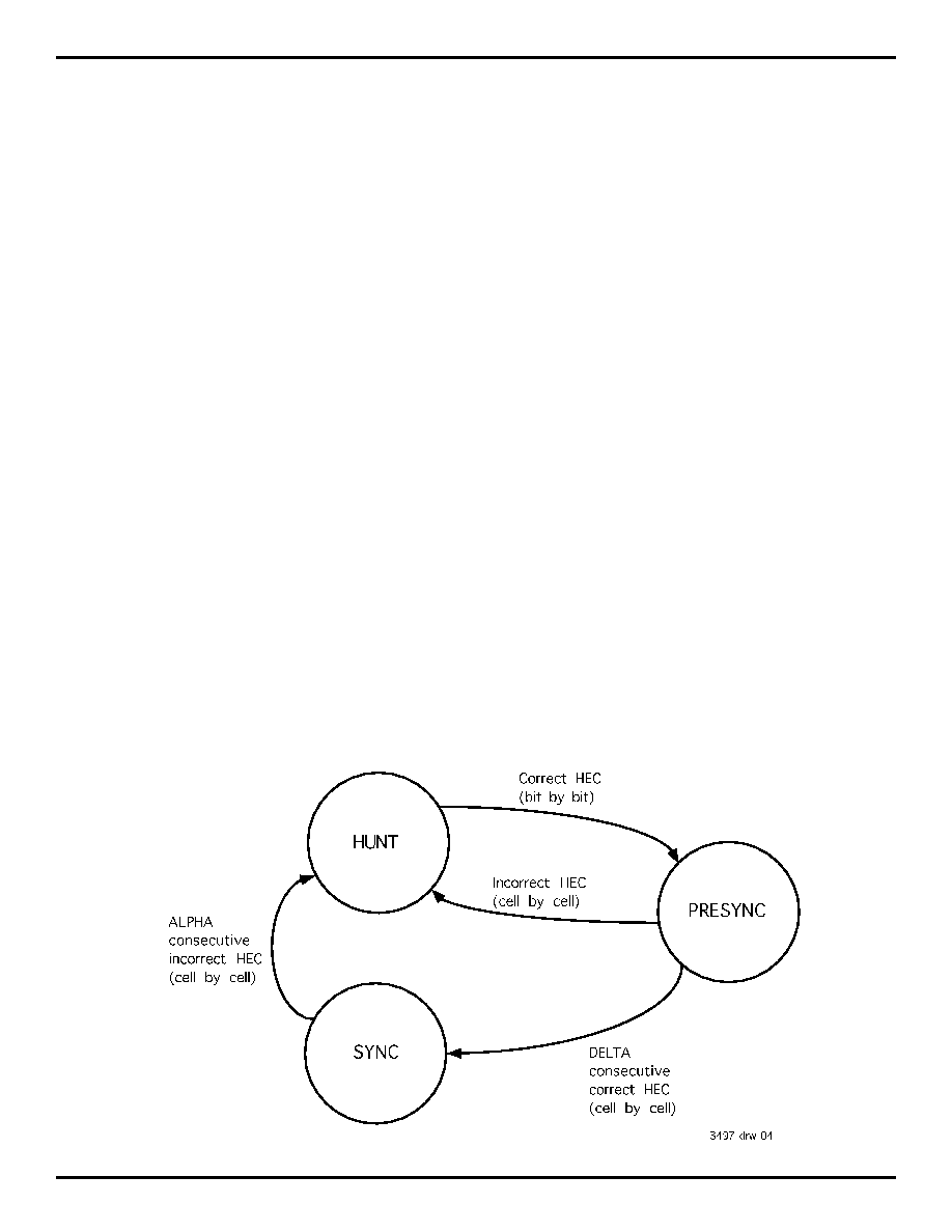
Cell Delineation is for validating the HEC of a cell header
by checking with the CRC-8 calculation over first 4 bytes of
ATM cell header; the coset value of "55h" can be optionally
added to the HEC during validation. HEC validation uses the
state machine in CCITT recommendation I.432 and is shown
in Figure 1.
The state machine shown in Figure 1 is initialized to the
HUNT state in which every byte of ATM 53 byte is checked
for a valid HEC. Once correct HEC has been found, cell
delineation state machine enters the PRESYNC state that
validates HEC on a cell by cell basis. If additional DELTA
(value is suggested to be six) consecutive correct HECs are
validated, the state machine enters the SYNC state. How-
ever, if any incorrect HEC is found in the PRESYNC state, the
state machine reverts to HUNT state. Once in SYNC state, it
stays in the SYNC state until ALPHA (value is suggested to be
seven) consecutive incorrect HECs are detected. HUNT state
is entered and the search for a correct HEC on a byte by byte
basis resumes.
Cell could be discarded with HEC errors by using HEC

8.03
12
IDT77155
ADVANCED INFORMATION
155Mbps ATM PHY (TC-PMD) USER NETWORK INTERFACE
Commercial Temperature Range
verification while in SYNC state. The HEC verification state
machine is shown in Figure 2. The state machine is initialized
to "correction mode". Cells with no HEC errors are passed to
the receive FIFO. Any single bit error detected in the incoming
cell headers are corrected and the cells are passed. It enters
into "detection mode" if any single bit or multi-bit errors in the
header are detected. In "detection mode", all cells with single
or multi-bit errors are dropped. Only cells with no errors are
passed. When a cell with no HEC error is detected in "detec-
tion mode", it enters back to "correction mode". However, if
seven consecutive cells with errored HEC are received,
HUNT state is entered from the "detection mode".
The ATM Descrambler descrambles the incoming 48 byte
cell payload only (header is not descrambled) by using poly-
nomial x
43
+ 1. The descrambling function may be disabled.
One 8-bit saturating HEC correctable error counter, one 8-
bit saturating HEC uncorrectable error counter, and a 19-bit
saturating receive cell counter are provided for ATM Cell
performance monitoring .
The HEC correctable error counter accumulates HEC
single bit errors in the header. The HEC uncorrectable error
counter accumulates HEC multiple bit errors in the header.
The receive cell counter accumulates the number of assigned
cells. All counters are active only in the SYNC state.
These three counter are to be read via microprocessor
interface at least once per second for performance monitor-
ing.
The received GFC bits are output in a serial stream via the
GFC Extraction output. GFC bits are extracted for every
received cell with the RCP output to indicate the position of the
most significant bit. The GFC output may be disabled via the
control register or no cell delineation.
The Receive FIFO has four ATM cells depth. It provides
FIFO management and the separation of STS-3c or STS-1
timing from ATM layer timing.
The FIFO management functions are to fill the receive four
cells FIFO and indicate when cells are ready to be read from
the receive FIFO and to detect FIFO overflow and underflow.
When overflow, the receive FIFO discards the incoming ATM
cells, a maskable interrupt and status register also active for
overflow condition. When underflow, the read is ignored.
When FIFO data is read out by RFCLK, the start of cell
(RSOC) is active. The cell available status (RCA) is provided
to indicate a cell is available in the receive FIFO.
CLOCK SYNTHESIS
The Clock Generator generates the 155.52 or 51.84 MHz
transmit clock by locking to a 1/8-frequency reference clock
i.e., synthesized from a 19.44 MHz or 6.48 MHz reference
clock.
PARALLEL TO SERIAL
This block performs the parallel to serial conversion to
convert the outgoing byte serial data to bit serial data.
TRANSMIT SONET FRAMER
The Transmit SONET Framer provides framing pattern
(A1, A2) insertion, scrambling, pointer generation, SONET
section, line and path overhead insertion, and alarm signal
insertion.
The Framing pattern (A1, A2) and C1 are inserted into
outgoing STS-3c or STS-1 data stream. The framing bit error
may be insert for diagnostic.
The STS Scrambler scrambles the outgoing data except
framing bytes (A1, A2) and identity byte (C1) by the using
polynomial 1 + x
6
+ x
7
. Scrambling may be disabled via control
register. An "all-zero" pattern may be inserted via micropro-
cessor interface after scrambling for diagnostic information.
The outgoing section BIP-8 error detection code (B1) is
calculated over all bits of the complete STS-3c or STS-1 frame
after scrambling by bit interleaved parity calculation using
even parity. The calculated BIP-8 code is then inserted into
the B1 byte of the next outgoing frame before scrambling.
Corrupted BIP-8 code may be inserted via control register for
diagnostic information.
The Line AIS may be set for outgoing data stream by
inserting "all-one" pattern into line overhead and Synchro-
nous Payload Envelope (SPE) of STS-3c or STS-1 frame by
control register via microprocessor interface.
The Line Remote Defect Indication (RDI) may be set for
outgoing data stream by inserting "110" pattern in bits 6-8 of
K2 byte to generate Line RDI.
K1 and K2 byte may be inserted for outgoing data stream
for automatic switch protection (APS) use.
The outgoing line BIP-8 error detection code (B2) is calcu-
lated over all bits of the line overhead and Synchronous
Payload Envelope (SPE) of STS-3c or STS-1 frame before
scrambling by bit interleaved parity calculation using even
parity. The calculated BIP-8 code is then inserted to the B2
byte of the next outgoing frame before scrambling. Corrupted
BIP-8 code may be inserted via control register for diagnostic
information.
The Line FEBE can be inserted by accumulating detected
B2 BIP-8 errors from receive direction into FEBE code of the
third Z2 byte for transmit STS-3c frame.
The Pointer Generator generates the pointer (H1, H2) for
outgoing STS-3c or STS-1 data stream. The "ss" bits of
pointer is programmable for the SDH requirement. The loca-
tion of start of the Synchronous Payload Envelope (SPE) is
according to the value of generated pointer.
IIDT77155
ADVANCED INFORMATION
155Mbps ATM PHY (TC-PMD) USER NETWORK INTERFACE
Commercial Temperature Range
8.03
13
The outgoing path BIP-8 error detection code (B3) is
calculated over all bits of Synchronous Payload Envelope
(SPE) of STS-3c or STS-1 frame before scrambling by bit
interleaved parity calculation using even parity. The calcu-
lated BIP-8 code is then inserted to the B3 byte of the next
outgoing frame before scrambling. Corrupted BIP-8 code
may be inserted via control register for diagnostic.
The C2 byte is set as "13h" by default for ATM mapping.
Value of C2 may be set by control register via microprocessor.
The Path FEBE can be inserted by accumulating detected
B3 BIP-8 errors from receive direction into FEBE code of the
path status byte (G1) for transmit STS-3c or STS-1 frame.
Path FEBE may be inserted via control register for diagnostic
information.
The Path Remote Defect Indication (RDI) may be set for
outgoing data stream by inserting "1" into bit 5 of path status
byte (G1).
H4 can be inserted by the value, which indicates the offset
between H4 byte position and the ATM cell boundary of the
first cell at the same row.
Synchronous Payload Envelope (SPE) can be mapped
into outgoing STS-3c or STS-1 frame according to the gener-
ating pointer.
TRANSMIT UTOPIA CELL FIFO
The ATM Scrambler scrambles the out going 48 byte cell
payload only (header is not scrambled) by using polynomial
x
43
+ 1. The scrambling function may be disabled.
The Idle Cell Generator Block inserts idle/unassigned
cells into the transmit cell stream if a complete ATM cell was
not written into the transmit FIFO. The GFC, PTI and CLP
may be set via control registers. The "all-zero" pattern is
inserted into the VCI/VPI of header. HEC of the idle cell is
calculated and inserted.
The HEC Generator calculates the CRC-8 code over the
first four byte of header and inserts the CRC-8 code into the
fifth byte of header. The polynomial x
8
+ x
2
+ x + 1 for HEC
generation is used. The coset polynomial x
6
+ x
4
+ x
2
+ 1 is
added to the residue. A 19-bit saturating transmit cell
counter is provided for ATM cell performacne monitoring.
The four serial GFC bits are inserted according to the
framing pulse of the transmit cell. The value of GFC bits may
be set by the control registers.
The Transmit FIFO has four ATM cells depth. It provides
FIFO management and the separation of STS-3c or STS-1
timing from ATM layer timing.
The FIFO management functions are to fill the transmit
four cells FIFO and indicate when cells are ready to be written
into the transmit FIFO and to detect FIFO overflow condition.
When the transmit FIFO contains four cells and the upstream
device still writes cell into FIFO, the overflow condition will be
indicated. A maskable interrupt and status register also
active for overflow condition. The write signal and all data
writing into FIFO are ignored until there is a space in FIFO.
MICROPROCESSOR INTERFACE
The Microprocessor Interface provides interface logic
circuit and the registers for the functions of configuration,
monitoring, control and test.
Figure 1. Cell Delineation State Diagram

8.03
14
IDT77155
ADVANCED INFORMATION
155Mbps ATM PHY (TC-PMD) USER NETWORK INTERFACE
Commercial Temperature Range
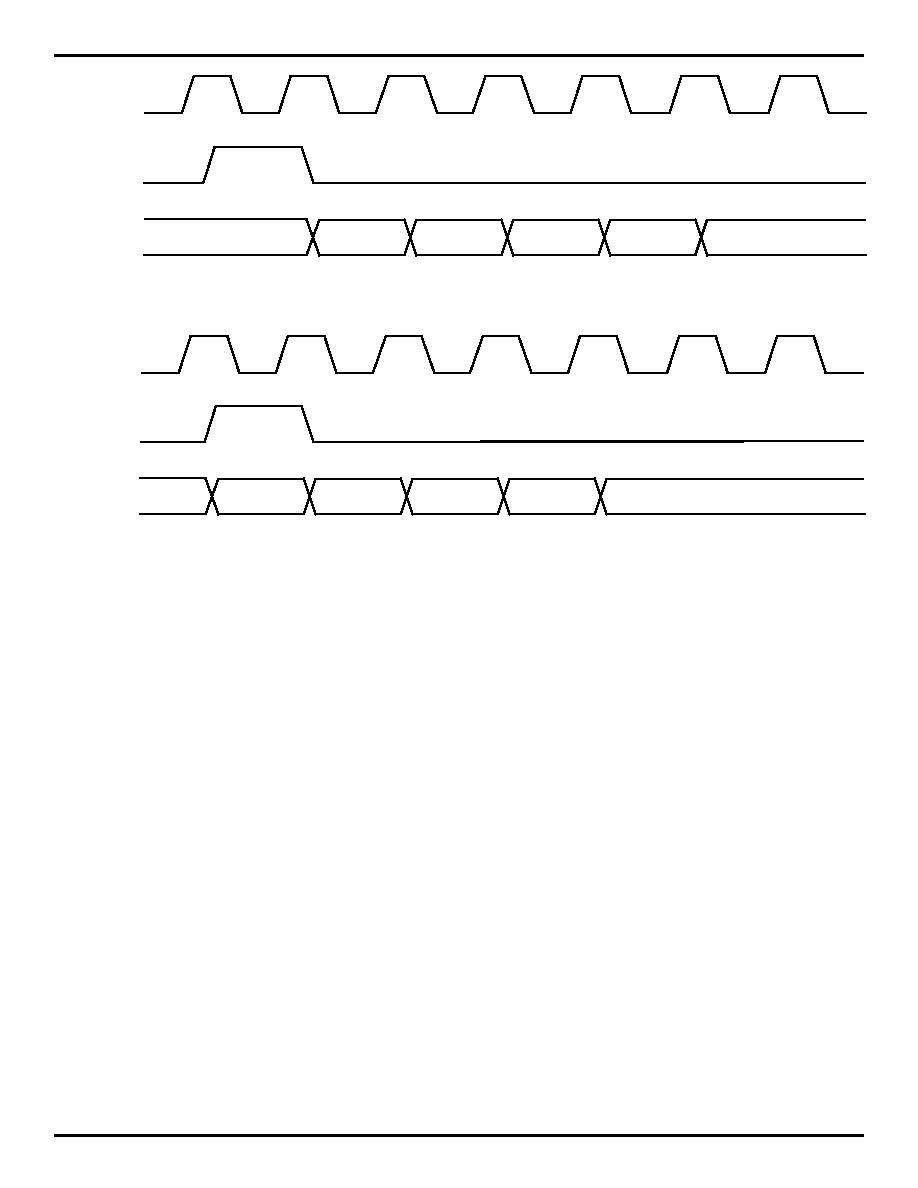
H2
P44
P45
P46
P47
P48
H1
TFCLK
TCA
TSOC
TDAT[0:7]
TXPRTY
H1
TCALEVEL0 = 1
X
X
X
3497 drw 08
X
Figure 2. HEC Verification State Diagram
Figure 3. Transmit Waveform for UTOPIA Interface
H2
P44
P45
P46
P47
P48
H1
RFCLK
RCA
RSOC
RDAT[0:7]
RXPRTY
H1
RCALEVEL0 = 0
3497 drw 09
Z
X
X
Figure 4. Re-
IIDT77155
ADVANCED INFORMATION
155Mbps ATM PHY (TC-PMD) USER NETWORK INTERFACE
Commercial Temperature Range
8.03
15
TCLK
TGFC
TCP
GFC[3]
GFC[2]
GFC[1]
GFC[0]
X
X
3497 drw 10
RCLK
RGFC
RCP
GFC[3]
GFC[2]
GFC[1]
GFC[0]
X
X
3497 drw 11
Figure 6. Receive GFC Serial Link Waveform
Figure 5. Transmit GFC Serial Link Waveform
8.03
16
IDT77155
ADVANCED INFORMATION
155Mbps ATM PHY (TC-PMD) USER NETWORK INTERFACE
Commercial Temperature Range
OPERATION MODES
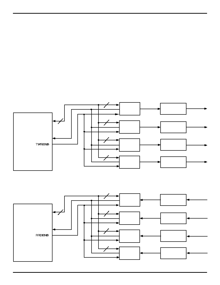
MULTI-PHY OPERATION
Multiple IDT77155s may be connected to common bus
when a Multi-PHY system architecture is needed.
Both Transmit and Receive UTOPIA busses, as well as the
utility bus, can attach to common busses.
Device selection is controlled via the UTOPIA "enable"
control signals ( TWRENB, RRDENB) and Multi-PHY ad-
dressing signals (TXADDR[1:0], RXADDR[1:0]). In transmit,
TWRENB tells the selected device (selected by TXADDR[1:0])
that the data and control signals it sees are to be used for ATM
cell transmission. In receive, when RRDENB is not asserted
(active low), RDAT[7:0], RXPRTY, RSOC, and RCA are all tri-
stated, allowing them to share a common bus. When RRDENB
is asserted, the selected device (selected by RXADDR[1:0])
drives these outputs, transferring the data to the upstream
hardware.
∑ Loopback
The IDT77155 supports two loopback functions that are
enabled by control bits in the control register.
∑ Local Loopback
The local loopback mode provides a connection within the
PHY between transmit and receive data. This loopback con-
nects the high speed transmit data and clock to the high speed
receive data and clock as shown in Figure 9. Note that while
this mode is operating, no data is forwarded to or received
from the line interface.
∑ Line Loopback
The line loopback might also be called "remote loopback"
since it provides for a means to test the overall system,
including the line. The line loopback connects the high speed
receive data and clock to the transmit data and clock as shown
in Figure 10.
"Upstream"
Hardware
77155#1
Optical
Transceiver
77155#2
77155#3
77155#4
"UTOPIA Transmit Bus"
--TDAT[7:0]
--TXPRTY
--TSOC
--TXADDR[1:0]
77155 drw 12
12
12
12
12
12
Optical
Transceiver
Optical
Transceiver
Optical
Transceiver
TCA
"Upstream"
Hardware
77155#1
Optical
Transceiver
77155#2
77155#3
77155#4
"UTOPIA Receive Bus"
--RDAT[7:0]
--RXPRTY
--RSOC
--RXADDR[1:0]
77155 drw 13
12
12
12
12
12
Optical
Transceiver
Optical
Transceiver
Optical
Transceiver
RCA
Figure 7. Multi-PHY: Transmit Direction
Figure 8. Multi-PHY: Receive Direction

IIDT77155
ADVANCED INFORMATION
155Mbps ATM PHY (TC-PMD) USER NETWORK INTERFACE
Commercial Temperature Range
8.03
17
Figure 10. Line Loopback
Encoder
Parallel
to
Serial
Transmit
SONET
Framer
Clk Gen.
Transmit
ATM
Cell
FIFO
Clk Rec.
Serial
to
Parallel
Receive
SONET
Framer
Decoder
Receive
UTOPIA
Cell
FIFO
Encoder
Clk Rec.
RRCLK+
RRCLK-
ALOS+
ALOS-
RXD+
RXD-
RXDO+
RXDO-
RBYP
RCLK
RGFC
RCA
TxADDR[1:0]
TRCLK+
TRCLK-
TXD+
TXD-
TXC+
TXC-
TBYP
RATE0
TCLK
TCP
Transmit
UTOPIA
Cell
FIFO
MPHYEN
APT1
LF≠
LF+
LFO
RALM
RFP
RCP
ATP2
RATE1
TFPO
XOFF
TGFC
TCA
TSOC
TDAT[7:0]
TXPRTY
TFCLK
RSOC
RDAT[7:0]
RXPRTY
RFCLK
TSEN
RxADDR[1:0]
3497 drw 07
Micoprocessor
Interface
D[7:0]
A[7:0]
ALE
Encoder
Parallel
to
Serial
Transmit
SONET
Framer
Clk Gen.
Transmit
ATM
Cell
FIFO
Clk Rec.
Serial
to
Parallel
Receive
SONET
Framer
Decoder
Receive
UTOPIA
Cell
FIFO
Encoder
Clk Rec.
RRCLK+
RRCLK-
ALOS+
ALOS-
RXD+
RXD-
RXDO+
RXDO-
RBYP
RCLK
RGFC
RCA
TxADDR[1:0]
TRCLK+
TRCLK-
TXD+
TXD-
TXC+
TXC-
TBYP
RATE0
TCLK
TCP
Transmit
UTOPIA
Cell
FIFO
MPHYEN
APT1
LF≠
LF+
LFO
RALM
RFP
RCP
ATP2
RATE1
TFPO
XOFF
TGFC
TCA
TSOC
TDAT[7:0]
TXPRTY
TFCLK
RSOC
RDAT[7:0]
RXPRTY
RFCLK
TSEN
RxADDR[1:0]
3497 drw 06
Micoprocessor
Interface
D[7:0]
A[7:0]
ALE
RST
Figure 9. Local Loopback

8.03
18
IDT77155
ADVANCED INFORMATION
155Mbps ATM PHY (TC-PMD) USER NETWORK INTERFACE
Commercial Temperature Range
REGISTER LISTING
Address Register
0X00
Master Reset & ID Register
0X01
Configuration Register
0X02
Interrupt Register
0X04
Master Clock Monitor Register
0X05
Master Control Register
0X06
Transmit Clock Synthesis Control/Status Register
0X07
Receive Clock/Data Recovery Control/Stuts Register
0X10
Receive Section Overhead Control Register
0X11
Receive Section Overhead Status Register
0X12
Receive Section BIP Error Counter (LSB)
0X13
Receive Section BIP Error Counter (MSB)
0X14
Transmit Section Overhead Control Register
0X15
Transmit Section Overhead Control Register
0X18
Receive Line Overhead Status Register
0X19
Receive Line Overhead Interrupt Register
0X1A
Receive Line BIP Error Counter (LSB)
0X1B
Receive Line BIP Error Counter
0X1C
Receive Line BIP Error Counter (MSB)
0X1D
Receive Line FEBE Counter (LSB)
0X1E
Receive Line FEBE Counter
0X1F
Receive Line FEBE Counter (MSB)
0X20
Transmit Line Overhead Stutus Register
0X21
Transmit Line Overhead Control Register
0X24
Transmit K1 Byte Register
0X25
Transmit K2 Byte Register
0X26
Receive K1 Byte Register
0X27
Receive K2 Byte Register
0X30
Receive Path Overhead Status Register
0X31
Receive Path Overhead Interrupt Register
0X33
Receive Path Overhead Interrupt Enable Register
0X37
Receive Path Signal Lable Byte Register
0X38
Receive Path BIP Error Counter (LSB)
0X39
Receive Path BIP Error Counter (MSB)
0X3A
Receive Path FEBE Counter (LSB)
0X3B
Receive Path FEBE Counter (MSB)
0X3D
Receive Path BIP Error Control Register
Address Register
0X40
Transmit Path Overhead Control Register
0X41
Tramsmit Pointer Control Register
0X45
Transmit Pointer LSB Register
0X46
Transmit Pointer MSB Register
0X48
Transmit Path Signal Lable Byte Register
0X49
Transmit Path Overhead Control Register
0X50
Receive Cell Control Register
0X51
Receive Cell Interrupts & Interrupt Enable Register
0X52
Receive Cell Match Header Register
0X53
Receive Cell Match Header Mask Register
0X54
Receive Cell Correctable Error Counter
0X55
Receive Cell Uncorrectable Error Counter
0X56
Receive Cell Counter (LSB)
0X57
Receive Cell Counter
0X58
Receive Cell Counter (MSB)
0X59
Receive Cell Configuration Register
0X5A
Receive ID Address Register
0X60
Transmit Cell Control Register
0X61
Transmit Cell Idle/Unassigned Cell Header Pattern
0X62
Transmit Cell Idle/Unassigned Cell Header Pattern
0X63
Transmit Cell Configuration Register
0X64
Transmit Cell Counter (LSB)
0X65
Transmit Cell Counter
0X66
Transmit Cell Counter (MSB)
0X67
Transmit Cell Configuration Register
0X68
Transmit ID Address Register
0X70
Receive BER Status/Control Register
0X71
Receive BER Fail Threshold Register
0X72
Receive BER Fail Window Register
0X73
Receive BER Fail Denominator Register (LSB)
0X74
Receive BER Fail Denominator Register (MSB)
0X75
Receive BER Warning Threshold Register
0X76
Receive BER Warning Window Register
0X77
Receive BER Warning Denominator Register (LSB)
0X78
Receive BER Warning Denominator Register (MSB)
0X7F
Output PECL Control Register

IIDT77155
ADVANCED INFORMATION
155Mbps ATM PHY (TC-PMD) USER NETWORK INTERFACE
Commercial Temperature Range
8.03
19
CONFIGURATION, CONTROL AND STATUS REGISTERS
MASTER RESET & ID REGISTER
DEFAULT = 8'B00110000
ADDRESS 0X00
Bit
Type
Symbol
Function
Bit 7
R/W
mstReset
Software reset control. A logic one resets entire sonet digital logic, and a
logic zero has to be written to clear software reset. It resets the whole
chip into a low-power stand-by mode. A hardware reset sets the whole
register to its default state.
Bit 6
R
type[2]
Type value for the identification of chip.
Bit 5
R
type[1]
Type value for the identification of chip.
Bit 4
R
type[0]
Type value for the identification of chip.
Bit 3
R
id[3]
Revision ID number.
Bit 2
R
id[2]
Revision ID number.
Bit 1
R
id[1]
Revision ID number.
Bit 0
R
id[0]
Revision ID number.
CONFIGURATION REGISTER DEFAULT = 8'B01110000
ADDRESS 0X01
Bit
Type
Symbol
Function
Bit 7
--
--
Reserved
Bit 6
R/W
autoFEBE
Controls assertion of far end block errors (FEBE) in the transmit stream
upon detection of line and path error events. When set to logic one, path
FEBE errors are inserted in the transmit stream for each line or path BIP
error event in the receive stream. When deasserted, no such errors are
inserted.
Bit 5
R/W
autoLRDI
Controls assertion of line remote defect indication (LRDI) upon detection
of alarms. When set to a logic one, a line RDI is inserted into the transmit
stream upon detection of LOS, LOF, or LAIS in the receive stream.
Bit 4
R/W
autoPRDI
Controls assertion of path remote defect indication (PRDI) upon detection
of alarms. When set to a logic one, PRDI is inserted into the transmit
stream upon detection of an LOS, LOF, LAIS, LOP, PAIS, or LOC
signal.
Bit 3
R/W
TCAInv
Select active polarity of TCA signal. Default is the TCA signal being
active high.
Bit 2
R/W
RCAInv
Select active polarity of RCA signal. Default is the RCA signal being
active high.
Bit 1
R/W
RXDInv
Select active polarity of the RXD+/- inputs. Default selects RXD+ to be
active high and RXD- to be active low.
Bit 0
--
--
Reserved

8.03
20
IDT77155
ADVANCED INFORMATION
155Mbps ATM PHY (TC-PMD) USER NETWORK INTERFACE
Commercial Temperature Range
INTERRUPT REGISTER
DEFAULT = 8'BXXXXXXXX
ADDRESS 0X02
Bit
Type
Symbol
Function
Bit 7
R
txOOLInt
Transmit reference out of lock interrupt status indication. It indicates the
transmit clock synthesis PLL is unable to lock to the reference frequency
TRCLK+/-. This bit is cleared when the register is read.
Bit 6
R
rxLOCInt
Asserted when the loss of cell delineation (LOC) signal changes state.
This bit is reset after a read to this register.
Bit 5
R
rxOOLInt
Receive data out of lock interrupt status indication. It indicates the receive
clock/data recovery PLL's recovered clock is not within Bellcore's
requirement of frequency variation with respect to the reference clock
RRCLK+/-. It is also asserted if no transitions have occurred on the
RXD+/- inputs for 80 bit periods. This bit is cleared when the register is
read.
Bit 4
R
txCDi
Interrupt is asserted upon the detection of an interrupt from the tx cell
delineation block.
Bit 3
R
rxCDi
Interrupt is asserted upon the detection of an interrupt from the rx cell
delineation block.
Bit 2
R
rxPOHi
Interrupt is asserted upon the detection of an interrupt from the rx path
overhead section of the transmission convergence block.
Bit 1
R
rxLOHi
Interrupt is asserted upon the detection of an interrupt from the rx line
overhead section of the transmission convergence block.
Bit 0
R
rxSOHi
Interrupt is asserted upon the detection of an interrupt from the rx section
overhead section of the transmission convergence block.
MASTER CLOCK MONITOR REGISTER
DEFAULT = 8'BXXXXXXXX
ADDRESS 0X04
Bit
Type
Symbol
Function
Bit 7
--
--
Reserved
Bit 6
--
--
Reserved
Bit 5
--
--
Reserved
Bit 4
--
--
Reserved
Bit 3
R
rrclkReg
RRCLK+/- monitor. Set on the rising edge of RRCLK+/-. Cleared when
this register is read.
Bit 2
R
trclkReg
TRCLK+/- monitor. Set on the rising edge of TRCLK+/-. Cleared when
this register is read.
Bit 1
R
rclkReg
RCLK monitor. Set on the rising edge of the output clock RCLK. Cleared
when this register is read.
Bit 0
R
tclkReg
TCLK monitor. Set on the rising edge of the output clock TCLK. Cleared
when this register is read.

IIDT77155
ADVANCED INFORMATION
155Mbps ATM PHY (TC-PMD) USER NETWORK INTERFACE
Commercial Temperature Range
8.03
21
MASTER CONTROL REGISTER
DEFAULT = 8'B00100000
ADDRESS 0X05
Bit
Type
Symbol
Function
Bit 7
R/W
rxLOCIEn
Loss of cell delineation interrupt enable. When set to a logic one, the
INTB signal of the chip is asserted when a change in the LOC signal
occurs.
Bit 6
R
LOC
Loss of cell delineation (LOC) indication.
Bit 5
R/W
txFixptr
Set payload pointer at 522 and disable any pointer movement. (Default = 1)
Bit 4
--
--
Reserved
Bit 3
--
--
Reserved
Bit 2
R/W
txLLoop
Line loopback enable. When a logic one, TXD+/- are connected internally
to RXD+/-.
Bit 1
R/W
rxDLoop
Diagnostic loopback enable. The serial output and clock streams are
connected internally to the serial input streams.
Bit 0
R/W
rxLoopT
Loop time operation enable. When a logic one, the transmitter clock is the
recovered receive clock when RBYP is disabled, or RRCLK+/- when
RBYP is asserted. By default, the transmit clock is derived from TRCLK+/-.
TRANSMIT CLOCK SYNTHESIS CONTROL/STATUS REGISTER
DEFAULT = 8'B0000X000
ADDRESS 0X06
Bit
Type
Symbol
Function
Bit 7
--
--
Reserved
Bit 6
--
--
Reserved
Bit 5
--
--
Reserved
Bit 4
--
--
Reserved
Bit 3
R
txOOL
Transmit out of lock status signal indicating the transmit clock synthesis
logic is unable to lock to the reference clock TRCLK+/-.
Bit 2
--
--
Reserved
Bit 1
R/W
txOOLIEn
Interrupt enable for the transmit out of lock indication.
Bit 0
R/W
txrefSel
Selects the expected frequency of TRCLK+/-. If a logic 0, the reference
frequency is 19.44 MHz, else the reference frequency must be 6.48 MHz.
It affects the clock synthesis frequency only when TBYP is deasserted.
RECEIVE CLOCK/DATA RECOVERY CONTROL/STATUS REGISTER
DEFAULT = 8'B0000X000
ADDRESS 0X07
Bit
Type
Symbol
Function
Bit 7
--
--
Reserved
Bit 6
--
--
Reserved
Bit 5
--
--
Reserved
Bit 4
--
--
Reserved
Bit 3
R
rxOOL
Receive out of lock status signal indicating the receive clock/data recovery
logic is unable to lock to the input data stream. It is asserted if the
recovered clock is not within 244ppm of the reference clock RRCLK+/- or
if there are no transitions on the RXD+/- inputs for 80n bit periods.
Bit 2
--
--
Reserved
Bit 1
R/W
rxOOLIEn
Interrupt enable for the receive out of lock indication.
Bit 0
R/W
rxrefSel
Selects the expected frequency of RRCLK+/-. If a logic 0, the reference
frequency is 19.44 MHz, else the reference frequency must be 6.48 MHz.
It affects the clock/data recovery logic frequency only when RBYP is
deasserted.

8.03
22
IDT77155
ADVANCED INFORMATION
155Mbps ATM PHY (TC-PMD) USER NETWORK INTERFACE
Commercial Temperature Range
RECEIVE SECTION OVERHEAD CONTROL REGISTER
DEFAULT = 8'B00000000
ADDRESS 0X10
Bit
Type
Symbol
Function
Bit 7
--
--
Reserved
Bit 6
R/W
scrDis
Disable receive frame scrambler if set to logic one.
Bit 5
W
frcOOF
When set to logic one, the receive section overhead logic is forced out of
frame at the next frame boundary.
Bit 4
--
--
Reserved
Bit 3
R/W
B1ErrIEn
Interrupt enable for rx section BIP (B1) error. When asserted, an interrupt
is generated if section BIP (B1) error is detected.
Bit 2
R/W
LOSIEn
Receive loss of signal interrupt enable. When asserted, an interrupt is
generated if LOS alarm changes state.
Bit 1
R/W
LOFIEn
Receive loss of frame interrupt enable. When set to logic one, an interrupt
is generated if LOF alarm changes state.
Bit 0
R/W
OOFIEn
Receive out of frame interrupt enable. When set to logic one, an interrupt
is generated if OOF alarm changes state.
RECEIVE SECTION OVERHEAD STATUS REGISTER DEFAULT = 8'BXXXXXXXX
ADDRESS 0X11
Bit
Type
Symbol
Function
Bit 7
R
C1Int
Interrupt bit set if received C1 bytes received do not correspond to 1, 2, 3
respectively. This bit is cleared when this register is read.
Bit 6
R
B1ErrInt
Interrupt is asserted if section BIP (B1) errors received. This bit is cleared
when this register is read.
Bit 5
R
LOSInt
Loss of signal interrupt is asserted if LOS changes state. This bit is
cleared when this register is read.
Bit 4
R
LOFInt
Loss of frame interrupt is asserted if LOF changes state. This bit is
cleared when this register is read.
Bit 3
R
OOFInt
Out of frame interrupt is asserted if OOF changes state. This bit is
cleared when this register is read.
Bit 2
R
LOS
Loss of signal status indication. Asserted high.
Bit 1
R
LOF
Loss of frame status indication. Asserted high.
Bit 0
R
OOF
Out of frame status indication. Asserted high.
RECEIVE SECTION BIP ERROR COUNTER
DEFAULT = 16'HXXXX
ADDRESS 0X12
Bit
Type
Symbol
Function
Bit 7
R
B1ErrCnt[7]
B1 error counter bit
Bit 6
R
B1ErrCnt[6]
B1 error counter bit
Bit 5
R
B1ErrCnt[5]
B1 error counter bit
Bit 4
R
B1ErrCnt[4]
B1 error counter bit
Bit 3
R
B1ErrCnt[3]
B1 error counter bit
Bit 2
R
B1ErrCnt[2]
B1 error counter bit
Bit 1
R
B1ErrCnt[1]
B1 error counter bit
Bit 0
R
B1ErrCnt[0]
B1 error counter bit

IIDT77155
ADVANCED INFORMATION
155Mbps ATM PHY (TC-PMD) USER NETWORK INTERFACE
Commercial Temperature Range
8.03
23
ADDRESS 0X13
Bit
Type
Symbol
Function
Bit 7
R
B1ErrCnt[15]
B1 error counter bit
Bit 6
R
B1ErrCnt[14]
B1 error counter bit
Bit 5
R
B1ErrCnt[13]
B1 error counter bit
Bit 4
R
B1ErrCnt[12]
B1 error counter bit
Bit 3
R
B1ErrCnt[11]
B1 error counter bit
Bit 2
R
B1ErrCnt[10]
B1 error counter bit
Bit 1
R
B1ErrCnt[9]
B1 error counter bit
Bit 0
R
B1ErrCnt[8]
B1 error counter bit
NOTE:
1. B1ErrCnt[15:0] Receive section overhead BIP (B1) error counter. Cumulative error counter keeping track of errors from the previous poll of these registers.
The error count is polled by writing to either register or to address `h00. Such a write transfers accumulated errors to a holding register which may be read
later, and the registers are cleared. This transfer and reset of the registers are done such that coincident events are not lost. All error registers in the receive
sections of the transmission convergence block or the cell delineation block may be polled by a write to the master register `h00.
TRANSMIT SECTION OVERHEAD CONTROL REGISTER
DEFAULT = 8'B00000000
ADDRESS 0X14
Bit
Type
Symbol
Function
Bit 7
--
--
Reserved
Bit 6
R/W
scrDis
Disable transmit frame scrambler. Scrambling enabled if logic zero.
Bit 5
--
--
Reserved
Bit 4
--
--
Reserved
Bit 3
--
--
Reserved
Bit 2
--
--
Reserved
Bit 1
--
--
Reserved
Bit 0
R/W
LAISIns
Insert line alarm signal (LAIS) in transmit stream. Line alarm results in all bits
except the section overhead bytes being set to logic 1 prior to scrambling.
TRANSMIT SECTION OVERHEAD CONTROL REGISTER
DEFAULT = 8'B00000000
ADDRESS 0X15
Bit
Type
Symbol
Function
Bit 7
--
--
Reserved
Bit 6
--
--
Reserved
Bit 5
--
--
Reserved
Bit 4
--
--
Reserved
Bit 3
--
--
Reserved
Bit 2
R/W
LOSIns
Insert loss of signal into transmit stream. The transmit stream is forced to
all zeroes if this bit is asserted.
Bit 1
R/W
B1Inv
Invert B1 byte before insertion into transmit stream. controls error
insertion into the section B1 byte.
Bit 0
R/W
frErrIns
Insert framing error. Inserts a single bit error continuously into the most
significant bit of the A1 section overhead byte. When this bit is set to
logic one, the A1 bytes transmitted are 0x76 instead of 0xf6.

8.03
24
IDT77155
ADVANCED INFORMATION
155Mbps ATM PHY (TC-PMD) USER NETWORK INTERFACE
Commercial Temperature Range
RECEIVE LINE OVERHEAD STATUS REGISTER
DEFAULT = 8'B00000000
ADDRESS 0X18
Bit
Type
Symbol
Function
Bit 7
R/W
B2Word
Controls accumulation of B2 errors. If set to logic one, the B2 error counter
is incremented only once per frame for one or more errors received during
that frame. When disabled, the B2 error counter is incremented by the
received error count during that frame. Max B2 errors is 8 per frame for
STS-1 and 24 for STS-3c per frame.
Bit 6
--
--
Reserved
Bit 5
--
--
Reserved
Bit 4
--
--
Reserved
Bit 3
--
--
Reserved
Bit 2
--
--
Reserved
Bit 1
R
LAIS
Receive line alarm signal status indication.
Bit 0
R
LRDI
Receive line remote defect indication status indication.
RECEIVE LINE OVERHEAD INTERRUPT REGISTER DEFAULT = 8'B0000XXXX
ADDRESS 0X19
Bit
Type
Symbol
Function
Bit 7
R/W
LFEBEIEn
Receive line FEBE (Z2) error interrupt enable. If set to logic one, an
interrupt is generated if a line FEBE is detected.
Bit 6
R/W
B2ErrIEn
Receive line BIP (B2) error interrupt enable. If set to logic one, an
interrupt is generated if a line BIP (B2) error is detected.
Bit 5
R/W
LAISIEn
Receive line alarm indication signal interrupt enable. If set to logic one, an
interrupt is generated if LAIS changes state.
Bit 4
R/W
LRDIIEn
Receive line RDI error interrupt enable. If set to logic one, an interrupt is
generated if line RDI signal changes state.
Bit 3
R
LFEBEInt
Receive line FEBE (Z2) error interrupt is asserted when a line FEBE
is detected. Cleared when this register is read.
Bit 2
R
B2ErrInt
Receive line BIP error interrupt is asserted when a B2 error is detected.
Cleared when this register is read.
Bit 1
R
LAISInt
Receive line alarm interrupt is asserted when a change in the line alarm
signal (LAIS) occurs. Cleared when this register is read.
Bit 0
R
LRDIInt
Receive line RDI interrupt is asserted when a change in the line RDI
signal occurs. Cleared when this register is read.
RECEIVE LINE OVERHEAD BIP ERROR COUNTER
DEFAULT = 20'HXXXXX
ADDRESS 0X1A
Bit
Type
Symbol
Function
Bit 7
R
B2ErrCnt[7]
B2 error counter bit
Bit 6
R
B2ErrCnt[6]
B2 error counter bit
Bit 5
R
B2ErrCnt[5]
B2 error counter bit
Bit 4
R
B2ErrCnt[4]
B2 error counter bit
Bit 3
R
B2ErrCnt[3]
B2 error counter bit
Bit 2
R
B2ErrCnt[2]
B2 error counter bit
Bit 1
R
B2ErrCnt[1]
B2 error counter bit
Bit 0
R
B2ErrCnt[0]
B2 error counter bit

IIDT77155
ADVANCED INFORMATION
155Mbps ATM PHY (TC-PMD) USER NETWORK INTERFACE
Commercial Temperature Range
8.03
25
ADDRESS 0X1B
Bit
Type
Symbol
Function
Bit 7
R
B2ErrCnt[15]
B2 error counter bit
Bit 6
R
B2ErrCnt[14]
B2 error counter bit
Bit 5
R
B2ErrCnt[13]
B2 error counter bit
Bit 4
R
B2ErrCnt[12]
B2 error counter bit
Bit 3
R
B2ErrCnt[11]
B2 error counter bit
Bit 2
R
B2ErrCnt[10]
B2 error counter bit
Bit 1
R
B2ErrCnt[9]
B2 error counter bit
Bit 0
R
B2ErrCnt[8]
B2 error counter bit
ADDRESS 0X1C
Bit
Type
Symbol
Function
Bit 7
--
--
Reserved
Bit 6
--
--
Reserved
Bit 5
--
--
Reserved
Bit 4
--
--
Reserved
Bit 3
R
B2ErrCnt[19]
B2 error counter bit
Bit 2
R
B2ErrCnt[18]
B2 error counter bit
Bit 1
R
B2ErrCnt[17]
B2 error counter bit
Bit 0
R
B2ErrCnt[16]
B2 error counter bit
NOTE:
1. B2ErrCnt[19:0] BIP error counter of the receive line overhead section (B2
errors). Cumulative error counter keeping track of errors from the previous
poll of these registers. The error count is polled by writing to either of the
registers, or either of the Z2 error registers, or to address `h00. Such a write
transfers accumulated errors to a holding register which may be read later,
and the registers are cleared. This transfer and reset of the registers are
done such that coincident events are not lost. All error registers in the
receive sections of the transmission convergence block or the cell
delineation block may be polled by a write to the master register `h00.
RECEIVE LINE FEBE COUNTER
DEFAULT = 20'HXXXXX
ADDRESS 0X1D
Bit
Type
Symbol
Function
Bit 7
R
FEBECnt[7]
FEBE counter bit
Bit 6
R
FEBECnt[6]
FEBE counter bit
Bit 5
R
FEBECnt[5]
FEBE counter bit
Bit 4
R
FEBECnt[4]
FEBE counter bit
Bit 3
R
FEBECnt[3]
FEBE counter bit
Bit 2
R
FEBECnt[2]
FEBE counter bit
Bit 1
R
FEBECnt[1]
FEBE counter bit
Bit 0
R
FEBECnt[0]
FEBE counter bit
ADDRESS 0X1E
Bit
Type
Symbol
Function
Bit 7
R
FEBECnt[15]
FEBE counter bit
Bit 6
R
FEBECnt[14]
FEBE counter bit
Bit 5
R
FEBECnt[13]
FEBE counter bit
Bit 4
R
FEBECnt[12]
FEBE counter bit
Bit 3
R
FEBECnt[11]
FEBE counter bit
Bit 2
R
FEBECnt[10]
FEBE counter bit
Bit 1
R
FEBECnt[9]
FEBE counter bit
Bit 0
R
FEBECnt[8]
FEBE counter bit
ADDRESS 0X1F
Bit
Type
Symbol
Function
Bit 7
--
--
Reserved
Bit 6
--
--
Reserved
Bit 5
--
--
Reserved
Bit 4
--
--
Reserved
Bit 3
R
FEBECnt[19]
FEBE counter bit
Bit 2
R
FEBECnt[18]
FEBE counter bit
Bit 1
R
FEBECnt[17]
FEBE counter bit
Bit 0
R
FEBECnt[16]
FEBE counter bit
NOTE:
1. FEBECnt[19:0] FEBE (Far End Block Error in receive Z2) counter of the
receive line overhead section. Cumulative error counter keeping track of
errors from the previous poll of these registers. The error count is polled
by writing to either of the registers, or either of the B2 error registers, or to
address `h00. Such a write transfers accumulated errors to a holding
register which may be read later, and the registers are cleared. This
transfer and reset of the registers are done such that coincident events are
not lost. All error registers in the receive sections of the transmission
convergence block or the cell delineation block may be polled by a write
to the master register `h00

8.03
26
IDT77155
ADVANCED INFORMATION
155Mbps ATM PHY (TC-PMD) USER NETWORK INTERFACE
Commercial Temperature Range
TRANSMIT K2 BYTE REGISTER
DEFAULT = 8'B00000000
ADDRESS 0X25
Bit
Type
Symbol
Function
Bit 7
R/W
K2Ins[7]
K2 Insertion Bit 7
Bit 6
R/W
K2Ins[5]
K2 Insertion Bit 5
Bit 4
R/W
K2Ins[4]
K2 Insertion Bit 4
Bit 3
R/W
K2Ins[3]
K2 Insertion Bit 3
Bit 2
R/W
K2Ins[2]
K2 Insertion Bit 2
Bit 1
R/W
K2Ins[1]
K2 Insertion Bit 1
Bit 0
R/W
K2Ins[0]
K2 Insertion Bit 0
NOTE:
1. k2Ins[7:0] Value to be inserted into the K2 byte of transmit stream.
Continuously inserts this value into the transmit stream. However, the
least significant 4 bits of the K2 byte in the transmit stream is overridden
by the path RDI value and the line FERF value if error conditions are
detected in the receive section of the transmission convergence logic.
RECEIVE K1 BYTE REGISTER
DEFAULT = 8'BXXXXXXXX
ADDRESS 0X26
Bit
Type
Symbol
Function
Bit 7
R
K1[7]
Receive K1 Bit 7
Bit 6
R
K1[6]
Receive K1 Bit 6
Bit 5
R
K1[5]
Receive K1 Bit 5
Bit 4
R
K1[4]
Receive K1 Bit 4
Bit 3
R
K1[3]
Receive K1 Bit 3
Bit 2
R
K1[2]
Receive K1 Bit 2
Bit 1
R
K1[1]
Receive K1 Bit 1
Bit 0
R
K1[0]
Receive K1 Bit 0
NOTE:
1. k1[7:0] K1 byte of receive stream. Updated if new K1 byte received for 3
consecutive frames.
RECEIVE K2 BYTE REGISTER
DEFAULT = 8'BXXXXXXXX
ADDRESS 0X27
Bit
Type
Symbol
Function
Bit 7
R
K2[7]
Receive K2 Bit 7
Bit 6
R
K2[6]
Receive K2 Bit 6
Bit 5
R
K2[5]
Receive K2 Bit 5
Bit 4
R
K2[4]
Receive K2 Bit 4
Bit 3
R
K2[3]
Receive K2 Bit 3
Bit 2
R
K2[2]
Receive K2 Bit 2
Bit 1
R
K2[1]
Receive K2 Bit 1
Bit 0
R
K2[0]
Receive K2 Bit 0
NOTE:
1. k2[7:0] K2 byte of receive stream. Updated if new K2 byte received for 3
consecutive frames
TRANSMIT LINE OVERHEAD STATUS REGISTER
DEFAULT = 8'B00000000
ADDRESS 0X20
Bit
Type
Symbol
Function
Bit 7
--
--
Reserved
Bit 6
--
--
Reserved
Bit 5
--
--
Reserved
Bit 4
--
--
Reserved
Bit 3
--
--
Reserved
Bit 2
--
--
Reserved
Bit 1
--
--
Reserved
Bit 0
R/W
LRDI
Transmit line RDI
insertion into transmit
stream. When set to
logic one, line RDI is
inserted by transmitting
the code 110 into the 3
least significant bits of
the K2 byte of the
transmit stream.
TRANSMIT LINE OVERHEAD CONTROL REGISTER
DEFAULT = 8'B00000000
ADDRESS 0X21
Bit
Type
Symbol
Function
Bit 7
--
--
Reserved
Bit 6
--
--
Reserved
Bit 5
--
--
Reserved
Bit 4
--
--
Reserved
Bit 3
--
--
Reserved
Bit 2
--
--
Reserved
Bit 1
--
--
Reserved
Bit 0
R/W
B2Inv
When set to logic one,
B2 byte is inverted
before insertion into
transmit stream.
TRANSMIT K1 BYTE REGISTER
DEFAULT = 8'B00000000
ADDRESS 0X24
Bit
Type
Symbol
Function
Bit 7
R/W
K1Ins[7]
K1 Insertion Bit 7
Bit 6
R/W
K1Ins[6]
K1 Insertion Bit 6
Bit 5
R/W
K1Ins[5]
K1 Insertion Bit 5
Bit 4
R/W
K1Ins[4]
K1 Insertion Bit 4
Bit 3
R/W
K1Ins[3]
K1 Insertion Bit 3
Bit 2
R/W
K1Ins[2]
K1 Insertion Bit 2
Bit 1
R/W
K1Ins[1]
K1 Insertion Bit 1
Bit 0
R/W
K1Ins[0]
K1 Insertion Bit 0
NOTE:
1. k1Ins[7:0] Value to be inserted into the K1 byte of transmit stream.
Continuously inserts this value into the transmit stream.

IIDT77155
ADVANCED INFORMATION
155Mbps ATM PHY (TC-PMD) USER NETWORK INTERFACE
Commercial Temperature Range
8.03
27
RECEIVE PATH OVERHEAD STATUS REGISTER
DEFAULT = 8'B00X0XX00
ADDRESS 0X30
Bit
Type
Symbol
Function
Bit 7
--
--
Reserved
Bit 6
--
--
Reserved
Bit 5
R
LOP
Receive loss of pointer (LOP) status indication.
Bit 4
--
--
Reserved
Bit 3
R
PAIS
Receive path alarm indication (PAIS) status signal.
Bit 2
R
PRDI
Receive path remote path indication status indication.
Bit 1
--
--
Reserved
Bit 0
--
--
Reserved
RECEIVE PATH OVERHEAD INTERRUPT REGISTER DEFAULT = 8'BX0X0XXXX
ADDRESS 0X31
Bit
Type
Symbol
Function
Bit 7
R
C2Int
C2 label bytes error interrupt. Asserted when the expected C2 value is
not received for 5 consecutive frames. The C2byte register (`h37) stores
the most recently received C2 byte.
Bit 6
--
--
Reserved
Bit 5
R
LOPInt
Loss of pointer interrupt et when a change in LOP signal occurs. Cleared
when this register is read.
Bit 4
--
--
Reserved
Bit 3
R
PAISInt
Path alarm indication signal interrupt is asserted when a change in the
PAIS signal occurs. Cleared when this register is read.
Bit 2
R
PRDIInt
Path RDI interrupt is asserted when a change in the path RDI signal
occurs. Cleared when this register is read.
Bit 1
R
B3ErrInt
Path BIP (B3) error interrupt is asserted when a path BIP (B3) error is
detected. Cleared when this register is read.
Bit 0
R
PFEBEInt
Path FEBE (bit 1-4 of G1) interrupt is asserted when a path FEBE is
detected. Cleared when this register is read.
RECEIVE PATH OVERHEAD INTERRUPT ENABLE REGISTER
DEFAULT = 8'B00000000
ADDRESS 0X33
Bit
Type
Symbol
Function
Bit 7
R/W
C2IEn
C2 signal label bytes error interrupt enable If set to logic one, an interrupt
is generated if a C2 error is detected. C2 error occurs when unexpected
C2 bytes are received for 5 consecutive frames.
Bit 6
--
--
Reserved
Bit 5
R/W
LOPIEn
Loss of pointer interrupt enable. If set to logic one, an interrupt is generated
if a LOP change is detected.
Bit 4
--
--
Reserved
Bit3
R/W
PAISIEn
Path alarm indication signal interrupt enable. If set to logic one, an
interrupt is generated if a PAIS change is detected.
Bit 2
R/W
PRDIIEn
Path RDI interrupt enable. If set to logic one, an interrupt is generated if a
path RDI change is detected.
Bit 1
R/W
B3ErrIEn
Path BIP (B3) error interrupt enable. If set to logic one, an interrupt is
generated if a path BIP (B3) error is detected.
Bit 0
R/W
PFEBEIEn
Path FEBE (bit 1-4 of G1) interrupt enable. If set to logic one, an interrupt
is generated if a path FEBE is detected.

8.03
28
IDT77155
ADVANCED INFORMATION
155Mbps ATM PHY (TC-PMD) USER NETWORK INTERFACE
Commercial Temperature Range
RECEIVE PATH SIGNAL LABEL BYTE REGISTER
DEFAULT = 8'BXXXXXXXX
ADDRESS 0X37
Bit
Type
Symbol
Function
Bit 7
R
C2rx[7]
Receive C2 Bit 7
Bit 6
R
C2rx[6]
Receive C2 Bit 6
Bit 5
R
C2rx[5]
Receive C2 Bit 5
Bit 4
R
C2rx[4]
Receive C2 Bit 4
Bit 3
R
C2rx[3]
Receive C2 Bit 3
Bit 2
R
C2rx[2]
Receive C2 Bit 2
Bit 1
R
C2rx[1]
Receive C2 Bit 1
Bit 0
R
C2rx[0]
Receive C2 Bit 0
NOTE:
1. C2rx[7:0] most recent errored path label byte received which led to the C2
interrupt.
RECEIVE PATH OVERHEAD BIP ERROR COUNTER
DEFAULT = 16'HXXXX
ADDRESS 0X38
Bit
Type
Symbol
Function
Bit 7
R
B3ErrCnt[7]
B3 error counter bit
Bit 6
R
B3ErrCnt[5]
B3 error counter bit
Bit 4
R
B3ErrCnt[4]
B3 error counter bit
Bit 3
R
B3ErrCnt[3]
B3 error counter bit
Bit 2
R
B3ErrCnt[2]
B3 error counter bit
Bit 1
R
B3ErrCnt[1]
B3 error counter bit
Bit 0
R
B3ErrCnt[0]
B3 error counter bit
ADDRESS 0X39
Bit
Type
Symbol
Function
Bit 7
R
B3ErrCnt[15]
B3 error counter bit
Bit 6
R
B3ErrCnt[14]
B3 error counter bit
Bit 5
R
B3ErrCnt[13]
B3 error counter bit
Bit 4
R
B3ErrCnt[12]
B3 error counter bit
Bit 3
R
B3ErrCnt[11]
B3 error counter bit
Bit 2
R
B3ErrCnt[10]
B3 error counter bit
Bit 1
R
B3ErrCnt[9]
B3 error counter bit
Bit 0
R
B3ErrCnt[8]
B3 error counter bit
NOTE:
1. B3ErrCnt Receive path overhead BIP (B3) error counter. Cumulative
error counter keeping track of errors from the previous poll of these
registers. The error count is polled by writing to either of the registers, or
either of the RDI error registers, or to address `h00. Such a write transfers
accumulated errors to a holding register which may be read later, and the
registers are cleared. This transfer and reset of the registers are done
such that coincident events are not lost. All error registers in the receive
sections of the transmission convergence block or the cell delineation
block may be polled by a write to the master register `h00
RECEIVE PATH FEBE COUNTER
DEFAULT = 16'HXXXX
ADDRESS 0X3A
Bit
Type
Symbol
Function
Bit 7
R
PFEBECnt[7]
Path FEBE counter bit
Bit 6
R
PFEBECnt[5]
Path FEBE counter bit
Bit 4
R
PFEBECnt[4]
Path FEBE counter bit
Bit 3
R
PFEBECnt[3]
Path FEBE counter bit
Bit 2
R
PFEBECnt[2]
Path FEBE counter bit
Bit 1
R
PFEBECnt[1]
Path FEBE counter bit
Bit 0
R
PFEBECnt[0]
Path FEBE counter bit
ADDRESS 0X3B
Bit
Type
Symbol
Function
Bit 7
R
PFEBECnt[15]
Path FEBE counter bit
Bit 6
R
PFEBECnt[14]
Path FEBE counter bit
Bit 5
R
PFEBECnt[13]
Path FEBE counter bit
Bit 4
R
PFEBECnt[12]
Path FEBE counter bit
Bit 3
R
PFEBECnt[11]
Path FEBE counter bit
Bit 2
R
PFEBECnt[10]
Path FEBE counter bit
Bit 1
R
PFEBECnt[9]
Path FEBE counter bit
Bit 0
R
PFEBECnt[8]
Path FEBE counter bit
NOTE:
1. PFEBECnt[15:0] Receive path FEBE (Bit 1-4 of G1 byte) counter. Cumu-
lative error counter keeping track of errors from the previous poll of these
registers. The error count is polled by writing to either of the registers, or
either of the BIP (B3) error registers, or to address `h00. Such a write
transfers accumulated errors to a holding register which may be read later,
and the registers are cleared. This transfer and reset of the registers are
done such that coincident events are not lost. All error registers in the
receive sections of the transmission convergence block or the cell
delineation block may be polled by a write to the master register`h00.

IIDT77155
ADVANCED INFORMATION
155Mbps ATM PHY (TC-PMD) USER NETWORK INTERFACE
Commercial Temperature Range
8.03
29
RECEIVE PATH BIP ERROR CONTROL REGISTER
DEFAULT = 8'B00000000
ADDRESS 0X3D
Bit
Type
Symbol
Function
Bit 7
--
--
Reserved
Bit 6
--
--
Reserved
Bit 5
R/W
blkBIP
Controls accumulation of B3 errors. If set to logic one, the B3 error counter
is incremented only once per SPE for one or more errors received during
that frame. When disabled, the B3 error counter is incremented by the
received error count during that SPE. Max B3 errors is 8 per SPE.
Bit 4
--
--
Reserved
Bit 3
--
--
Reserved
Bit 2
--
--
Reserved
Bit 1
--
--
Reserved
Bit 0
--
--
Reserved
TRANSMIT PATH OVERHEAD CONTROL REGISTER
DEFAULT = 8'B00000000
ADDRESS 0X40
Bit
Type
Symbol
Function
Bit 7
--
--
Reserved
Bit 6
--
--
Reserved
Bit 5
--
--
Reserved
Bit 4
--
--
Reserved
Bit 3
--
--
Reserved
Bit 2
--
--
Reserved
Bit 1
R/W
B3Inv
Invert B3 byte before insertion into the transmission stream. When
set to a logic one, the B3 byte is inverted causing the insertion of 8 BIP
errors per frame. The B3 byte is uncorrupted when this bit is a logic zero.
Bit 0
R/W
PAISIns
Insert path alarm indication signal into the transmit stream. When a logic
one, the complete SPE, and the pointer bytes (H1, H2, & H3) are
overwritten with the all ones pattern.

8.03
30
IDT77155
ADVANCED INFORMATION
155Mbps ATM PHY (TC-PMD) USER NETWORK INTERFACE
Commercial Temperature Range
TRANSMIT POINTER CONTROL REGISTER
DEFAULT = 8'B00000000
ADDRESS 0X41
Bit
Type
Symbol
Function
Bit 7
--
--
Reserved
Bit 6
R/W
frcPtr
Force the insertion of the pointer values (H1 & H2 bytes) in the pointer registers
(`h45, `h46) into the transmit stream for diagnostics. The SPE
and other overheads are transmitted in a normal fashion although it would
not be extracted by the receiving logic due to an incorrect pointer. At least
one corrupted pointer is guaranteed to be sent.
Bit 5
R/W
stuffCtl
Stuff opportunity spacing between consecutive SPE stuff events. When
asserted to a logic one, stuff events controlled by
incPtr and decPtr is
generated at a maximum rate of once every four frames. Else, stuff
events may be generated every frame.
Bit 4
R/W
Ptr
Initialize pointer value of next frame with pointer value contained in `h45
and `h46. The registers at `h45 and `h46 are initialized before this bit is set
to a logic one. If a legal pointer value is loaded (0 <= pointer <= 782) then
the transmit pointer value is changed to this value with the SPE being
modified to this position appropriately. This bit is cleared once the new
pointer is loaded.
Bit 3
R/W
NDF
Controls insertion of the new data flags in `h46 into the transmit stream.
When asserted to a logic one, the pattern in `h46 is inserted continuously
in the payload pointer. When disabled, the normal pointer value (`b0110)
is inserted.
Bit 2
R/W
decPtr
Decrement pointer in the next immediate frame. This bit is cleared when
the new pointer value is inserted in the transmit stream. This bit has no
effect if the transmit
fixPtr bit is asserted.
Bit 1
R/W
incPtr
Increment pointer in the next immediate stream. This bit is cleared when
the new pointer value is inserted in the transmit stream. This bit has no
effect if the transmit
fixPtr bit is asserted.
Bit 7
--
--
Reserved
TRANSMIT POINTER LSB REGISTER
DEFAULT = 8'B00000000
ADDRESS 0X45
Bit
Type
Symbol
Function
Bit 7
R/W
arbPtr[7]
Arbitrary pointer Bit 7
Bit 6
R
arbPtr[6]
Arbitrary pointer Bit 6
Bit 5
R
arbPtr[5]
Arbitrary pointer Bit 5
Bit 4
R
arbPtr[4]
Arbitrary pointer Bit 4
Bit 3
R
arbPtr[3]
Arbitrary pointer Bit 3
Bit 2
R
arbPtr[2]
Arbitrary pointer Bit 2
Bit 1
R
arbPtr1]
Arbitrary pointer Bit 1
Bit 0
R
arbPtr[0]
Arbitrary pointer Bit 0
NOTE:
1. arbPtr[7:0] Payload pointer to be inserted into frame if
Ptr is set. A legal
value results in the transmit payload pointer changing to the correspond-
ing byte position. If the
frcPtr bit is set, the payload pointer changes to
this arbitrary value but the SPE position remains unchanged.

IIDT77155
ADVANCED INFORMATION
155Mbps ATM PHY (TC-PMD) USER NETWORK INTERFACE
Commercial Temperature Range
8.03
31
TRANSMIT POINTER MSB REGISTER DEFAULT = 8'B10010000
ADDRESS 0X46
Bit
Type
Symbol
Function
Bit 7
R/W
NDFVal[3]
New data flag field value to be inserted into the transmit stream if
ldPtr is
set or if
NDF bit is set.
Bit 6
R/W
NDFVal[2]
Bit 5
R/W
NDFVal[1]
Bit 4
R/W
NDFVal[0]
Bit 3
R/W
ssBit[1]
SONET/SDH switch bit and
ss bits value of the transmit stream. If
ssBit[1] is a logic high, then the chip transforms to full SDH mode. By
default (ssBit[1] = `0'), the chip follows the SONET specifications.
SONET mode: ssBit[1] = `0'
(1)
ss bits of pointer is set to "00" for transmit direction.
(2) Line AIS detection criteria.
AIS-L enter state: 5 consecutive frames with "111" in bits 6-8
of K2 byte are detected.
AIS-L exit state: 5 consecutive frames with pattern other than
"111" in bits 6-8 of K2 byte are detected.
(3) Line RDI detection criteria.
RDI-L enter state: 5 consecutive frames with "110" in bits 6-8
of K2 byte are detected.
RDI-L exit state: 5 consecutive frames with pattern other than
"110" in bits 6-8 of K2 byte are detected.
(4) Path BIP-8 calculation for STS-1 applications
Count 87 columns of SPE including 2 fixed stuffs column
(column 30 and 59).
(5) No consequent actions Line RDI for transmit direction by detection
of B2 EBER (refer to register address `h70 BERfail)
SDH mode: ssBit[1] = `1'
(1)
ss bits of pointer is set to "10" for transmit direction.
(2) Line AIS detection criteria.
AIS-L enter state: 3 consecutive frames with "111" in bits 6-8
of K2 byte are detected.
AIS-L exit state: 3 consecutive frames with pattern other than
"111" in bits 6-8 of K2 byte are detected.
(3) Line RDI detection criteria.
RDI-L enter state: 3 consecutive frames with "110" in bits 6-8
of K2 byte are detected.
RDI-L exit state: 3 consecutive frames with pattern other than
"110" in bits 6-8 of K2 byte are detected.
(4) Path BIP-8 calculation for STS-1 applications
Count 85 columns of SPE excluding 2 fixed stuffs column
(column 30 and 59).
(5) Generate consequent actions Line RDI for transmit direction by
detection of B2 EBER (refer to register address `h70 BERfail)
Bit 2
R/W
ssBit[0]
ss bits value of the transmit stream. ssBit[0] is set to `0'.
Bit 1
R/W
arbPtr[9]
most significant bits of the arbitrary payload pointer to be inserted into
frame if
ldPtr is set. A legal value results in the transmit payload pointer
changing to the corresponding byte position. If the
frcPtr bit is set, the
payload pointer changes to this arbitrary value but the SPE position
remains unchanged.
Bit 0
R/W
arbPtr[8]

8.03
32
IDT77155
ADVANCED INFORMATION
155Mbps ATM PHY (TC-PMD) USER NETWORK INTERFACE
Commercial Temperature Range
TRANSMIT PATH SIGNAL LABLE BYTE REGISTER
DEFAULT = 8'B00010011
ADDRESS 0X48
Bit
Type
Symbol
Function
Bit 7
R/W
C2tr[7]
Transmit C2 Bit 7
Bit 6
R/W
C2tr[6]
Transmit C2 Bit 6
Bit 5
R/W
C2tr[5]
Transmit C2 Bit 5
Bit 4
R/W
C2tr[4]
Transmit C2 Bit 4
Bit 3
R/W
C2tr[3]
Transmit C2 Bit 3
Bit 2
R/W
C2tr[2]
Transmit C2 Bit 2
Bit 1
R/W
C2tr[1]
Transmit C2 Bit 1
Bit 0
R/W
C2tr[0]
Transmit C2 Bit 0
NOTE:
1. C2tr[7:0]C2 value to be inserted into the transmit stream. Default value
is `h13 for ATM applications. Value may be changed for diagnostics
purposes.
TRANSMIT PATH OVERHEAD CONTROL REGISTER
DEFAULT = 8'B00000000
ADDRESS 0X49
Bit
Type
Symbol
Function
Bit 7
R/W
PFEBEIns[3]
Insert FEBE value into path status byte. This value is cleared after it has
been inserted into the path status byte for transmission. Any non-zero value
overrides the accumulated error values during the previous received frame.
If a non-zero value is read from this register, it implies that the transmission is
still pending.
Bit 6
R/W
PFEBEIns[2]
Bit 5
R/W
PFEBEIns[1]
Bit 4
R/W
PFEBEIns[0]
Bit 3
R/W
PRDIIns
Insert path remote defect indication into transmit stream. When set to a logic
one, the PRDI bit in the status byte is asserted. Once a PRDI indication is
sent, it is guaranteed to be sent asserted for 10 consecutive frames.
Bit 2
R/W
G1Ins[2]
G1 bits to be inserted into path status byte least significant bits.
Bit 2
R/W
G1Ins[1]
Bit 2
R/W
G1Ins[0]

IIDT77155
ADVANCED INFORMATION
155Mbps ATM PHY (TC-PMD) USER NETWORK INTERFACE
Commercial Temperature Range
8.03
33
RECEIVE CELL CONTROL REGISTER
DEFAULT = 8'B00000100
ADDRESS 0X50
Bit
Type
Symbol
Function
Bit 7
R
OCD
Out of cell delineation status indication. When asserted high, the cell
delineation state machine is in the
hunt or presync state.
Bit 6
R/W
parity
Select odd or even parity for RXPRTY output. When set to logic one, it is
even parity over the outputs RDAT[7:0], else it is odd parity.
Bit 5
R/W
pass
When enabled, filtering of cells with matching the pattern in cell header
register `h52 masked with the mask register `h53 is disabled. Filtering of field
with VPI = VCI = 0 is ignored and all cells are passed to the ATM layer.
Bit 4
R/W
corDis
Disables the HEC error correction algorithm. any error detected in the
incoming cell is treated as an uncorrectable error, and the cell is dropped.
Bit 3
R/W
HECdis
Controls the dropping of cells when an incorrectable HEC error is
detected. When disabled, cells with uncorrectable errors are dropped.
However, when set to a logic one, cells are passed to the TM layer
regardless of the errors detected. The HEC verification state machine is
always in the correction mode. cells are always dropped when the cell
delineation state machine is in the hunt or presync states.
Bit 2
R/W
csetAdd
Controls the addition of the coset polynomial. When a logic one, the coset
polynomial is added to the header prior to comparison.
Bit 1
R/W
scrDis
Controls the descrambling of the cell payload. When asserted high,
payload scrambling is disabled.
Bit 0
R/W
rxFIFOrst
Reset rx FIFO. Used to reset the four cell receive FIFO when asserted to
a logic one.The FIFO ignores all writes until this bit is cleared.
RECEIVE CELL INTERRUPTS & INTERRUPT ENABLE REGISTER
DEFAULT = 8'B000XXXX0
ADDRESS 0X51
Bit
Type
Symbol
Function
Bit 7
R/W
OCDIEn
Out of cell delineation interrupt enable. If set to logic one, an interrupt is
generated if an OCD change is detected
Bit 6
R/W
HECIEn
Correctable or incorrectable HEC error interrupt enable. If set to logic one,
an interrupt is generated if a correctable or uncorrectable error is detected
Bit 5
R/W
ovfIEn
FIFO overflow interrupt enable. If set to logic one, an interrupt is
generated if a FIFO overrun is detected
Bit 4
R
OCDInt
Out of cell delineation interrupt. Set when the OCD signal changes
value. This bit is cleared following a read to this register.
Bit 3
R
corInt
Correctable HEC error interrupt is asserted when a correctable HEC error is
detected. This bit is cleared following a read to this register.
Bit 2
R
uncorInt
Uncorrectable HEC error interrupt is asserted when an uncorrectable HEC error
is detected. This bit is cleared following a read to this register.
Bit 1
R
ovfInt
FIFO overflow interrupt is asserted when a receive FIFO overflow occurs. This
bit is cleared following a read to this register.
Bit 0
--
--
Reserved

8.03
34
IDT77155
ADVANCED INFORMATION
155Mbps ATM PHY (TC-PMD) USER NETWORK INTERFACE
Commercial Temperature Range
RECEIVE CELL MATCH HEADER REGISTER
DEFAULT = 8'B00000000
ADDRESS 0X52
Bit
Type
Symbol
Function
Bit 7
R/W
GFC[3]
GFC Bit 3 to match GFC of receive header
Bit 6
R/W
GFC[2]
GFC Bit 2 to match GFC of receive header
Bit 5
R/W
GFC[1]
GFC Bit 1 to match GFC of receive header
Bit 4
R/W
GFC[0]
GFC Bit 0 to match GFC of receive header
Bit 3
R/W
PTI[2]
PTI Bit 2 to match PTI of receive header
Bit 2
R/W
PTI[1]
PTI Bit 1 to match PTI of receive header
Bit 1
R/W
PTI[0]
PTI Bit 0 to match PTI of receive header
Bit 0
R/W
CLP
CLP value to match CLP of receive header
NOTE:
1. GFC[3:0], PTI[2:0], CLPMatch header pattern to match in the GFC, PTI, & CLP portion of the received header. Cells matching the unmasked bits of this
pattern, along with the criteria of VPI = VCI = 0, will be dropped. The receive pass bit control must be disabled to enable the dropping of idle/unassigned
cells.
RECEIVE CELL MATCH HEADER MASK REGISTER
DEFAULT = 8'B00000000
ADDRESS 0X53
Bit
Type
Symbol
Function
Bit 7
R/W
GFCmsk[3]
Mask GFC Bit 3
Bit 6
R/W
GFCmsk[2]
Mask GFC Bit 2
Bit 5
R/W
GFCmsk[1]
Mask GFC Bit 1
Bit 4
R/W
GFCmsk[0]
Mask GFC Bit 0
Bit 3
R/W
PTImsk[2]
Mask PTI Bit 2
Bit 2
R/W
PTImsk[1]
Mask PTI Bit 1
Bit 1
R/W
PTImsk[0]
Mask PTI Bit 0
Bit 0
R/W
CLPmsk
Mask CLP
NOTE:
1. GFCmsk[3:0], PTImsk[2:0], CLPmsk Mask bits for GFC, PTI, & CLP portion of the match header pattern. Cells matching the unmasked bits of the header
pattern register (`h52) will be dropped. A logic one in any bit position enables the corresponding bit in the pattern register to be compared. Note that the
VPI and VCI bits do not have a mask register. The pattern in them have to be a logic zero.
RECEIVE CELL CORRECTABLE ERROR COUNTER
DEFAULT = 8'BXXXXXXXX
ADDRESS 0X54
Bit
Type
Symbol
Function
Bit 7
R
corCnt[7]
Correctable HEC error count bit
Bit 6
R
corCnt[6]
Correctable HEC error count bit
Bit 5
R
corCnt[5]
Correctable HEC error count bit
Bit 4
R
corCnt[4]
Correctable HEC error count bit
Bit 3
R
corCnt[3]
Correctable HEC error count bit
Bit 2
R
corCnt[2]
Correctable HEC error count bit
Bit 1
R
corCnt[1]
Correctable HEC error count bit
Bit 0
R
corCnt[0]
Correctable HEC error count bit
NOTE:
1. corCnt [7:0] Correctable HEC error count register. This is a cumulative error counter keeping track of errors from the previous poll of these registers. The
error count is polled by writing to either of the HEC error registers (`h54 or `h55), or to address `h00. Such a write transfers accumulated errors to a holding
register which may be read later, and the registers are cleared. This transfer and reset of the registers are done such that coincident events are not lost.
All error registers in the receive sections of the transmission convergence block or the cell delineation block may be polled by a write to the master register
`h00.

IIDT77155
ADVANCED INFORMATION
155Mbps ATM PHY (TC-PMD) USER NETWORK INTERFACE
Commercial Temperature Range
8.03
35
RECEIVE CELL UNCORRECTABLE ERROR COUNTER
DEFAULT = 8'BXXXXXXXX
ADDRESS 0X55
Bit
Type
Symbol
Function
Bit 7
R
uncorCnt[7]
Uncorrectable HEC error count bit
Bit 6
R
uncorCnt[6]
Uncorrectable HEC error count bit
Bit 5
R
uncorCnt[5]
Uncorrectable HEC error count bit
Bit 4
R
uncorCnt[4]
Uncorrectable HEC error count bit
Bit 3
R
uncorCnt[3]
Uncorrectable HEC error count bit
Bit 2
R
uncorCnt[2]
Uncorrectable HEC error count bit
Bit 1
R
uncorCnt[1]
Uncorrectable HEC error count bit
Bit 0
R
uncorCnt[0]
Uncorrectable HEC error count bit
NOTE:
1. uncorCnt[7:0] Uncorrectable HEC error count register. This is a cumulative error counter keeping track of errors from the previous poll of these registers.
The error count is polled by writing to either of the HEC error registers (`h54 or `h55), or to address `h00. Such a write transfers accumulated errors to a
holding register which may be read later, and the registers are cleared. This transfer and reset of the registers are done such that coincident events are
not lost. All error registers in the receive sections of the transmission convergence blockor the cell delineation block may be polled by a write to the master
register `h00.
RECEIVE CELL COUNTER
DEFAULT = 19'H00000
ADDRESS 0X56
Bit
Type
Symbol
Function
Bit 7
R
cellCnt[7]
Receive cell counter bit
Bit 6
R
cellCnt[6]
Receive cell counter bit
Bit 5
R
cellCnt[5]
Receive cell counter bit
Bit 4
R
cellCnt[4]
Receive cell counter bit
Bit 3
R
cellCnt[3]
Receive cell counter bit
Bit 2
R
cellCnt[2]
Receive cell counter bit
Bit 1
R
cellCnt[1]
Receive cell counter bit
Bit 0
R
cellCnt[0]
Receive cell counter bit
ADDRESS 0X57
Bit
Type
Symbol
Function
Bit 7
R
cellCnt[15]
Receive cell counter bit
Bit 6
R
cellCnt[14]
Receive cell counter bit
Bit 5
R
cellCnt[13]
Receive cell counter bit
Bit 4
R
cellCnt[12]
Receive cell counter bit
Bit 3
R
cellCnt[11]
Receive cell counter bit
Bit 2
R
cellCnt[10]
Receive cell counter bit
Bit 1
R
cellCnt[9]
Receive cell counter bit
Bit 0
R
cellCnt[8]
Receive cell counter bit

8.03
36
IDT77155
ADVANCED INFORMATION
155Mbps ATM PHY (TC-PMD) USER NETWORK INTERFACE
Commercial Temperature Range
ADDRESS 0X58
Bit
Type
Symbol
Function
Bit 7
--
--
Reserved
Bit 6
--
--
Reserved
Bit 5
--
--
Reserved
Bit 4
--
--
Reserved
Bit 3
--
--
Reserved
Bit 2
R
cellCnt[18]
Receive cell counter bit
Bit 1
R
cellCnt[17]
Receive cell counter bit
Bit 0
R
cellCnt[16]
Receive cell counter bit
NOTE:
1.cellCnt [18:0] Receive cell counter of the number of cells passed thru' to the ATM. Cells filtered due to HEC errors or idle/unassigned cells are not counted.
This is a cumulative counter keeping track of rx cells from the previous poll of these registers. The count is polled by writing to either of these registers
(`h56, `h57, or `h58), the HEC error registers, or to address `h00. Such a write transfers accumulated errors to a holding register which may be read later,
and the registers are cleared. This transfer and reset of the registers are done such that coincident events are not lost. All error/count registers in the receive
sections of the transmission convergence block or the cell delineation block may be polled by a write to the master register `h00.
RECEIVE CELL CONFIGURATION REGISTER
DEFAULT = 8'B11111100
ADDRESS 0X59
Bit
Type
Symbol
Function
Bit 7
R/W
GFCen[3]
GFC enable bits. This determines which GFC bits are presented on the
RGFC output. If a GFCen bit is a logic one, the RGFC output presents
appropriate bit location the state of the associated GFC bit in the
current cell.
Bit 6
R/W
GFCen[2]
Bit 5
R/W
GFCen[1]
Bit 4
R/W
GFCen[0]
Bit 3
R/W
FixSen
Fixed stuff column control for STS-1 mode. When asserted high, the column
30 and 59 of the received SPE are assigned as fixed stuff columns. If FixSen is
low, Column 30 and 59 are assigned as ATM payload columns.
Bit 2
R/W
RCA level
RCA level control. When asserted to a logic one, a high to low transition on
RCA indicates the receive FIFO is empty. When a logic zero, a high to low
transition on RCA indicates the receive FIFO in almost empty and contains
only 4 more bytes to be read.
Bit 1
R/W
HECftr[1]
HEC filter bits. It indicates the number of consecutive error free cells
required in the detection mode before reverting back to the correction
mode, of the HEC verification state machine.
HECfltr[1:0]
Cell acceptance threshold
00
one ATM cell with correct HEC to revert to the
connection mode. This cell is accepted.
01
two ATM cells with correct HEC to revert to the
correction mode. The last cell is accepted
10
four ATM cells with correct HEC to revert to the
correction mode. The last cell is accepted
11
eight ATM cells with correct HEC to revert to the
correction mode. The last cell is accepted
Bit 0
R/W
HECftr[0]

IIDT77155
ADVANCED INFORMATION
155Mbps ATM PHY (TC-PMD) USER NETWORK INTERFACE
Commercial Temperature Range
8.03
37
RECEIVE ID ADDRESS REGISTER
DEFAULT = 8'B00000000
ADDRESS 0X5A
Bit
Type
Symbol
Function
Bit 7
--
--
Reserved
Bit 6
--
--
Reserved
Bit 5
--
--
Reserved
Bit 4
--
--
Reserved
Bit 3
--
--
Reserved
Bit 2
--
--
Reserved
Bit 1
R/W
IDAddr[1]
Device ID value for the receive portion of the receive UTOPIA logic. In
multi-PY mode, the appropriate receive UTOPIA signals are driven as
per UTOPIA level 2 protocol when the RXADDR bus value matches the
value in this register. This has no effect in single-PHY mode.
Bit 0
R/W
IDAddr[0]
TRANSMIT CELL CONTROL REGISTER
DEFAULT = 8'B00000100
ADDRESS 0X60
Bit
Type
Symbol
Function
Bit 7
R/W
fovrIEn
Transmit FIFO overrun interrupt enable. Enables the generation of an
interrupt due to a FIFO overrun or when the TSOC input is sampled high
during any position other than the first byte.
Bit 6
R
socInt
Start of cell interrupt. This bit is set high when the TSOC input is sampled high
during any position other than the first byte. When such a condition occurs, the
cell delineation logic assumes the new SOC signal is the start of a new cell,
and the previous few bytes are discarded.
Thus, cell delineation is performed in the transmit direction also. This bit is
cleared after a read of this register.
Bit 5
R
fovrInt
Transmit FIFO overrun interrupt. This bit is cleared after a read to this
register.
Bit 4
R/W
HECInv
Invert the HEC bytes before transmission for diagnostic purposes
when this bit is set to a logic one.
Bit 3
R/W
HECdis
Disables the generation & insertion of the of the header error check
sequence.
Bit 2
R/W
csetAdd
Controls the addition of the coset polynomial. When a logic one, the coset
polynomial is added to the header prior to transmission.
Bit 1
R/W
scrDis
Controls the descrambling of the cell payload. When asserted high,
payload scrambling is disabled.
Bit 0
R/W
txFIFOrst
Reset tx FIFO. Used to reset the four cell transmit FIFO when asserted
to a logic one. The FIFO ignores all writes until this bit is cleared.

8.03
38
IDT77155
ADVANCED INFORMATION
155Mbps ATM PHY (TC-PMD) USER NETWORK INTERFACE
Commercial Temperature Range
TRANSMIT CELL IDLE/UNASSIGNED CELL HEADER PATTERN
DEFAULT = 8'B00000000
ADDRESS 0X61
Bit
Type
Symbol
Function
Bit 7
R/W
GFCtx[3]
GFC Bit 3 to be inserted in GFC of transmit header for idle cell
Bit 6
R/W
GFCtx[2]
GFC Bit 2 to be inserted in GFC of transmit header for idle cell
Bit 5
R/W
GFCtx[1]
GFC Bit 1 to be inserted in GFC of transmit header for idle cell
Bit 4
R/W
GFCtx[0]
GFC Bit 0 to be inserted in GFC of transmit header for idle cell
Bit 3
R/W
PTItx[2]
PTI Bit 2 to be inserted in PTI of transmit header for idle cell
Bit 2
R/W
PTItx[1]
PTI Bit 1 to be inserted in PTI of transmit header for idle cell
Bit 1
R/W
PTItx[0]
PTI Bit 0 to be inserted in PTI of transmit header for idle cell
Bit 0
R/W
CLPtx
CLP value to be inserted in CLP of transmit header for idle cell
TRANSMIT CELL IDLE/UNASSIGNED CELL PAYLOAD PATTERN
DEFAULT = 8'B01101010
ADDRESS 0X62
Bit
Type
Symbol
Function
Bit 7
R/W
idlePaylaod[7]
Payload value bit 7 for transmit idle/unassigned cells
Bit 6
R/W
idlePaylaod[6]
Payload value bit 6 for transmit idle/unassigned cells
Bit 5
R/W
idlePaylaod[5]
Payload value bit 5 for transmit idle/unassigned cells
Bit 4
R/W
idlePaylaod[4]
Payload value bit 4 for transmit idle/unassigned cells
Bit 3
R/W
idlePaylaod[3]
Payload value bit 3 for transmit idle/unassigned cells
Bit 2
R/W
idlePaylaod[2]
Payload value bit 2 for transmit idle/unassigned cells
Bit 1
R/W
idlePaylaod[1]
Payload value bit 1 for transmit idle/unassigned cells
Bit 0
R/W
idlePaylaod[0]
Payload value bit 0 for transmit idle/unassigned cells
NOTE
1. idlePyload[7:0] payload octet of idle/unassigned cells. Idle/unassigned cells are transmitted when data cells are available to b transmitted in the tx FIFO.

IIDT77155
ADVANCED INFORMATION
155Mbps ATM PHY (TC-PMD) USER NETWORK INTERFACE
Commercial Temperature Range
8.03
39
TRANSMIT CELL CONFIGURATION REGISTER
DEFAULT = 8'B000X0000
ADDRESS 0X63
Bit
Type
Symbol
Function
Bit 7
R/W
parity
Select odd or even parity for TXPRTY input. When set to logic one, it is
even parity over the inputs TDAT[7:0], else it is odd parity.
Bit 6
R/W
parIEn
Transmit parity interrupt enable. When asserted, an interrupt is indicated
on the INTB output if a parity error is detected.
Bit 5
--
--
Reserved
Bit 4
R/W
parInt
tx parity interrupt. Set when a parity interrupt is detected. This bit is
cleared when this register is read.
Bit 3
R/W
FIFOdpth[1]
txFIFO depth control. When FIFO is filled to the specified depth, TCA is
disabled. TCA is asserted only when a complete cell has been read for
transmission. It is not recommended to set the FIFO depth to one cell. For
minimum latency and maximum throughput, set the FIFO depth to 2 cells.
FIFOdpth[1:0]
FIFO depth
00
4 cells
01
3 cells
10
2 cells
11
1 cell
Bit 2
R/W
FIFOdpth[0]
Bit 1
R/W
TCA level
TCA level control. When asserted to a logic one, a high to low transition
on TCA indicates the transmit FIFO is full. When a logic zero, a high to
low transition on TCA indicates the transmit FIFO in almost full and can
accept only 4 more bytes.
Bit 0
--
--
Reserved
TRANSMIT CELL COUNTER
DEFAULT = 19'H00000
ADDRESS 0X64
Bit
Type
Symbol
Function
Bit 7
R
txcellCnt[7]
Transmit cell counter bit
Bit 6
R
txcellCnt[6]
Transmit cell counter bit
Bit 5
R
txcellCnt[5]
Transmit cell counter bit
Bit 4
R
txcellCnt[4]
Transmit cell counter bit
Bit 3
R
txcellCnt[3]
Transmit cell counter bit
Bit 2
R
txcellCnt[2]
Transmit cell counter bit
Bit 1
R
txcellCnt[1]
Transmit cell counter bit
Bit 0
R
txcellCnt[0]
Transmit cell counter bit
ADDRESS 0X65
Bit
Type
Symbol
Function
Bit 7
R
txcellCnt[15]
Transmit cell counter bit
Bit 6
R
txcellCnt[14]
Transmit cell counter bit
Bit 5
R
txcellCnt[13]
Transmit cell counter bit
Bit 4
R
txcellCnt[12]
Transmit cell counter bit
Bit 3
R
txcellCnt[11]
Transmit cell counter bit
Bit 2
R
txcellCnt[10]
Transmit cell counter bit
Bit 1
R
txcellCnt[9]
Transmit cell counter bit
Bit 0
R
txcellCnt[8]
Transmit cell counter bit

8.03
40
IDT77155
ADVANCED INFORMATION
155Mbps ATM PHY (TC-PMD) USER NETWORK INTERFACE
Commercial Temperature Range
ADDRESS 0X66
Bit
Type
Symbol
Function
Bit 7
--
--
Reserved
Bit 6
--
--
Reserved
Bit 5
--
--
Reserved
Bit 4
--
--
Reserved
Bit 3
--
--
Reserved
Bit 2
R
txcellCnt[18]
Transmit cell counter bit
Bit 1
R
txcellCnt[17]
Transmit cell counter bit
Bit 0
R
txcellCnt[16]
Transmit cell counter bit
NOTE:
1. txcellCnt Transmit cell counter of the number of cells read from the transmit FIFO and inserted into the SPE. Idle/unassigned cells are not counted. This
is a cumulative counter keepingtrack of tx cells from the previous poll of these registers. The count is polled by writing to either of these registers (`h64,
`h65, or `h66), or to address `h00. Such a write transfers accumulated errors to a holding register which may be read later, and the registers are cleared.
This transfer and reset of the registers are done such that coincident events are not lost. All error/count registers in the transmit sections of the transmission
convergence block or the cell delineation block may be polled by a write tothe master register `h00.
TRANSMIT CELL CONFIGURATION REGISTER
DEFAULT = 8'B00001000
ADDRESS 0X67
Bit
Type
Symbol
Function
Bit 7
R/W
txGFCen[3]
GFC enable bits. This determines which GFC bits on the TGFC input are
accepted to be inserted into the transmit stream. If a GFCen bit is a logic one,
the corresponding GFC input is inserted into the appropriate bit position.
Bit 6
R/W
txGFCen[2]
Bit 5
R/W
txGFCen[1]
Bit 4
R/W
txGFCen[0]
Bit 3
R/W
txFixSen
Fixed stuff column control enable in STS-1. When asserted high, the
columns 30 and 59 of the transmitted SPE contains stuff bytes. The value
of the stuff byte is a fixed pattern selected by the
fixByte control.
Bit 2
R/W
H4InsDis
Disable the insertion of the calculated H4 byte. A value of 0 is inserted for
the H4 byte in the SPE.
Bit 1
R/W
fixByte[1]
byte pattern to be inserted into the fixed stuff columns of STS-1 SPE.
fixByte[1:0]
stuff bype pattern
00
`h00
01
`h55
10
`hAA
11
`hFF
Bit 0
R/W
fixByte[0]

IIDT77155
ADVANCED INFORMATION
155Mbps ATM PHY (TC-PMD) USER NETWORK INTERFACE
Commercial Temperature Range
8.03
41
TRANSMIT ID ADDRESS REGISTER
DEFAULT = 8'B00000000
ADDRESS 0X68
Bit
Type
Symbol
Function
Bit 7
--
--
Reserved
Bit 6
--
--
Reserved
Bit 5
--
--
Reserved
Bit 4
--
--
Reserved
Bit 3
--
--
Reserved
Bit 2
--
--
Reserved
Bit 1
R/W
txIDAddr[1]
Device ID value for the transmit portion of the transmit UTOPIA logic. In
multi-PHY mode, the appropriate transmit UTOPIA signals are driven as
per UTOPIA level 2 protocol when the TXADDR bus value matches the
value in this register. This has no effect in single-PHY mode.
Bit 0
R/W
txIDAddr[0]
RECEIVE BER STATUS/CONTROL REGISTER
DEFAULT = 8'B00000011
ADDRESS 0X70
Bit
Type
Symbol
Function
Bit 7
--
--
Reserved
Bit 6
--
--
Reserved
Bit 5
--
--
Reserved
Bit 4
--
--
Reserved
Bit 3
R/W
FailIEn
Interrupt enable for BER failure. Enables the generation of an interrupt
upon the detection of a BER failure condition.
Bit 2
R/W
WarnIEn
Interrupt enable for BER warning. Enables the generation of an interrupt
upon the detection of a BER warning condition.
Bit 1
R/W
BERfail
BER failure status indication. It is initially asserted at reset. Clearing this
bit triggers the BER failure algorithm. This bit is cleared when the register
is read. It is also as the indication of B2 EBER.
Bit 0
R/W
BERwarn
BER warning status indication. It is initially asserted at reset. Clearing this
bit triggers the BER warning algorithm. This bit is cleared when the
register is read.
RECEIVE BER FAIL THRESHOLD REGISTER
DEFAULT = 8'B00000000
ADDRESS 0X71
Bit
Type
Symbol
Function
Bit 7
R/W
ThldFail[7]
Value for the failure threshold of the BER fail algorithm.
Bit 6
R/W
ThldFail[6]
Bit 5
R/W
ThldFail[5]
Bit 4
R/W
ThldFail[4]
Bit 3
R/W
ThldFail[3]
Bit 2
R/W
ThldFail[2]
Bit 1
R/W
ThldFail[1]
Bit 0
R/W
ThldFail[0]

8.03
42
IDT77155
ADVANCED INFORMATION
155Mbps ATM PHY (TC-PMD) USER NETWORK INTERFACE
Commercial Temperature Range
RECEIVE BER FAIL WINDOW REGISTER
DEFAULT = 8'B00000000
ADDRESS 0X72
Bit
Type
Symbol
Function
Bit 7
R/W
WinFail[7]
Value for the window length of the BER fail algorithm.
Bit 6
R/W
WinFail[6]
Bit 5
R/W
WinFail[5]
Bit 4
R/W
WinFail[4]
Bit 3
R/W
WinFail[3]
Bit 2
R/W
WinFail[2]
Bit 1
R/W
WinFail[1]
Bit 0
R/W
WinFail[0]
RECEIVE BER FAIL DENOMINATOR REGISTER
DEFAULT = 16'H0000
ADDRESS 0X73
Bit
Type
Symbol
Function
Bit 7
R/W
DenFail[7]
LSB value for the deniminator count for the BER fail algorithm.
Bit 6
R/W
DenFail[6]
Bit 5
R/W
DenFail[5]
Bit 4
R/W
DenFail[4]
Bit 3
R/W
DenFail[3]
Bit 2
R/W
DenFail[2]
Bit 1
R/W
DenFail[1]
Bit 0
R/W
DenFail[0]
ADDRESS 0X74
Bit
Type
Symbol
Function
Bit 7
R/W
DenFail[15]
MSB value for the deniminator count for the BER fail algorithm.
Bit 6
R/W
DenFail[14]
Bit 5
R/W
DenFail[13]
Bit 4
R/W
DenFail[12]
Bit 3
R/W
DenFail[11]
Bit 2
R/W
DenFail[10]
Bit 1
R/W
DenFail[9]
Bit 0
R/W
DenFail[8]
RECEIVE BER WARNING THRESHOLD REGISTER
DEFAULT = 8'B00000000
ADDRESS 0X75
Bit
Type
Symbol
Function
Bit 7
R/W
ThldWarn[7]
Value for the failure threshold of the BER warning algorithm.
Bit 6
R/W
ThldWarn[6]
Bit 5
R/W
ThldWarn[5]
Bit 4
R/W
ThldWarn[4]
Bit 3
R/W
ThldWarn[3]
Bit 2
R/W
ThldWarn[2]
Bit 1
R/W
ThldWarn[1]
Bit 0
R/W
ThldWarn[0]

IIDT77155
ADVANCED INFORMATION
155Mbps ATM PHY (TC-PMD) USER NETWORK INTERFACE
Commercial Temperature Range
8.03
43
RECEIVE BER WARNING WINDOW REGISTER
DEFAULT = 8'B00000000
ADDRESS 0X76
Bit
Type
Symbol
Function
Bit 7
R/W
WinWarn[7]
Value for the window length of the BER warning algorithm.
Bit 6
R/W
WinWarn[6]
Bit 5
R/W
WinWarn[5]
Bit 4
R/W
WinWarn[4]
Bit 3
R/W
WinWarn[3]
Bit 2
R/W
WinWarn[2]
Bit 1
R/W
WinWarn[1]
Bit 0
R/W
WinWarn[0]
RECEIVE BER WARNING DENOMINATOR REGISTER
DEFAULT = 16'H0000
ADDRESS 0X77
Bit
Type
Symbol
Function
Bit 7
R/W
DenWarn[7]
LSB value for the deniminator count for the BER warning algorithm.
Bit 6
R/W
DenWarn[6]
Bit 5
R/W
DenWarn[5]
Bit 4
R/W
DenWarn[4]
Bit 3
R/W
DenWarn[3]
Bit 2
R/W
DenWarn[2]
Bit 1
R/W
DenWarn[1]
Bit 0
R/W
DenWarn[0]
ADDRESS 0X78
Bit
Type
Symbol
Function
Bit 7
R/W
DenWarn[15]
MSB value for the deniminator count for the BER warning algorithm.
Bit 6
R/W
DenWarn[14]
Bit 5
R/W
DenWarn[13]
Bit 4
R/W
DenWarn[12]
Bit 3
R/W
DenWarn[11]
Bit 2
R/W
DenWarn[10]
Bit 1
R/W
DenWarn[9]
Bit 0
R/W
DenWarn[8]
OUTPUT PECL CONTROL REGISTER
DEFAULT = 8'B00000000
ADDRESS 0X7F
Bit
Type
Symbol
Function
Bit 7
--
--
Reserved
Bit 6
--
--
Reserved
Bit 5
--
--
Reserved
Bit 4
--
--
Reserved
Bit 3
--
--
Reserved
Bit 2
R/W
pcctl_tc
PECL output control for TXC+/- output. If set to logic one, the output is
true PECL. the default is a rail-to-rail swing.
Bit 1
R/W
pcctl_td
PECL output control for TXD+/- output. If set to logic one, the output is
true PECL. the default is a rail-to-rail swing.
Bit 0
R/W
pcctl_r
PECL output control for RXDO+/- output. If set to logic one, the output is
true PECL. the default is a rail-to-rail swing.

8.03
44
IDT77155
ADVANCED INFORMATION
155Mbps ATM PHY (TC-PMD) USER NETWORK INTERFACE
Commercial Temperature Range
SYMBOL DISCRIPTION MIN. MAX. UNITS
TFCLK frequency
40
MHz
TFCLK duty cycle
40%
60%
%
RFCLK frequency
40
MHz
RFCLK duty cycle
40%
60%
%
Receive line clock duty cycle
40%
60%
%
Receive line clock duty cycle
40%
60%
%
tRSO
Receive clock RCLK to RCP/RGFC valid
2
15
ns
tALHD
Address to latch enable hold time
10
ns
tALSU
Address to latch enable setup time
20
ns
tARHD
Address to read hold time
5
ns
tARSU
Address to read setup time
25
ns
tAWHD
Address to write hold time
5
ns
tAWSU
Address to write setup time
25
ns
tBB
Time between consecutive operations
150
ns
tDT
Read to output data tristate
20
ns
tDWHD
Data to write hold time
1
ns
tDWSU
Data to write setup time
5
ns
tGHD
TGFC hold to TCLK
1
ns
tTHD
Input hold to TFCLK applies to TSOC, TWRENB, TDAT, and TXPRTY
1
ns
tRHD
Input hold to RFCLK applies to RRDENB
1
ns
tLRHD
Latch enable to read hold time
5
ns
tLRSU
Latch enable to read setup time
5
ns
tLW
Latch enable pulse width
20
ns
tLWHD
Latch enable to write hold time
5
ns
tLWSU
Latch enable to write setup time
5
ns
tTOV
TFCLK to output valid applies to TCA
1
20
ns
tROV
RFCLK to output valid applies to RSOC, RDAT, RCA, and RXPRTY
1
20
ns
tRD
Valid read to data propagation delay
80
ns
tRDHD
Receive data hold time (RBYP high)
1
ns
tGSO
Transmit clock TCLK to RCP valid
2
15
ns
tSOV
Transmit line clock output low to transmit differential data output
-2
2
ns
tRDSU
Receive data setup time (RBYP high)
2
ns
tTSU
Input setup to TFCLK applies to TSOC, TWRENB, TDAT, and TXPRTY
8
ns
tRSU
Input setup to RFCLK applies to RRDENB
8
ns
tGSU
TGFC set up to TCLK
10
ns
tWW
Write pulse width
40
ns
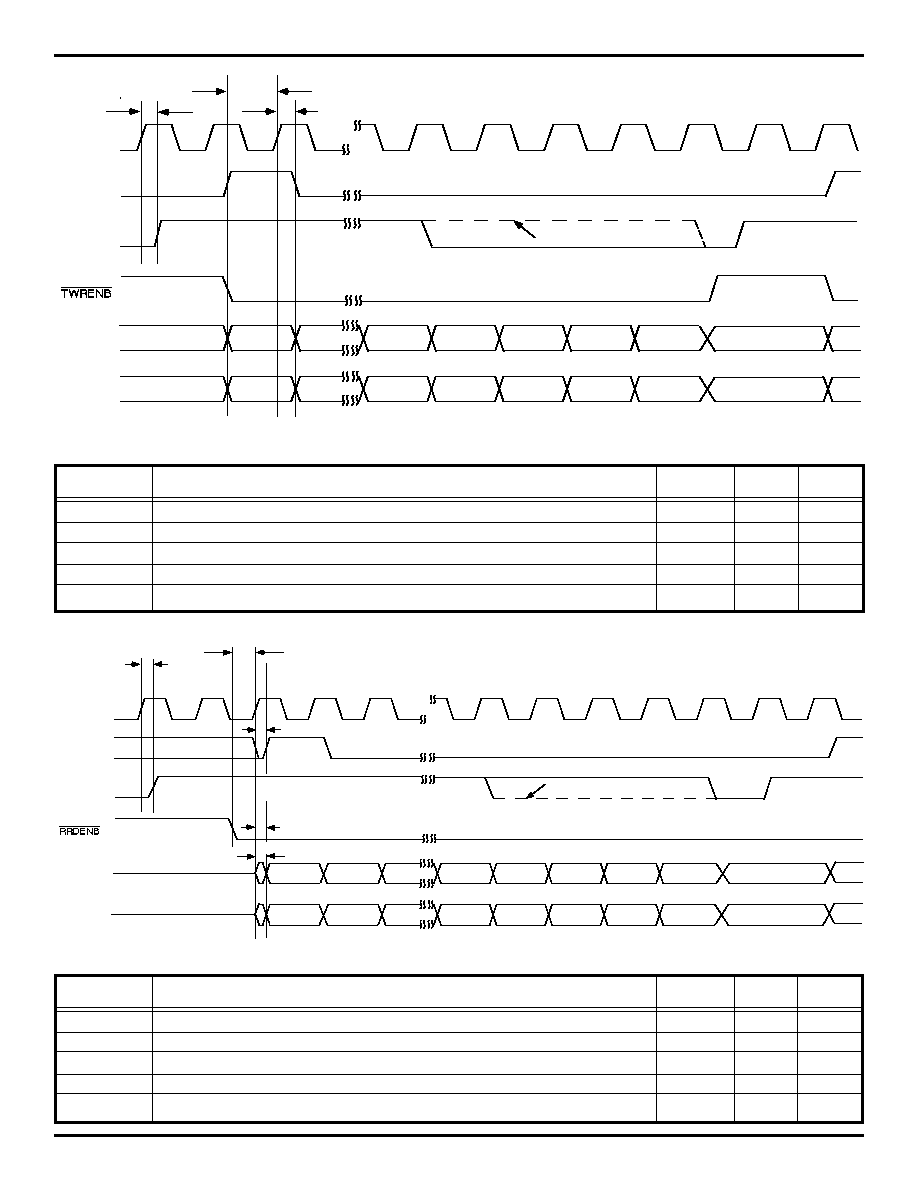
IIDT77155
ADVANCED INFORMATION
155Mbps ATM PHY (TC-PMD) USER NETWORK INTERFACE
Commercial Temperature Range
8.03
45
H2
P44
P45
P46
P47
P48
H1
TFCLK
TCA
TSOC
TDAT[0:7]
TXPRTY
H1
TCALEVEL0 = 1
X
X
X
3497 drw 14
X
t
TSU
t
THD
t
TOV
Figure 11. Transmit Timing for UTOPIA Interface
Figure 12. Receive Timing for UTOPIA Interface
SYMBOL DISCRIPTION MIN. MAX. UNITS
TFCLK frequency
40
MHz
TFCLK duty cycle
40%
60%
%
tTHD
Input hold to TFCLK applies to TSOC, TWRENB, TDAT, and TXPRTY
1
ns
tTOV
TFCLK to output valid applies to TCA
1
20
ns
tTSU
Input setup to TFCLK applies to TSOC, TWRENB, TDAT, and TXPRTY
8
ns
SYMBOL DISCRIPTION MIN. MAX. UNITS
RFCLK frequency
40
MHz
RFCLK duty cycle
40%
60%
%
tRHD
Input hold to RFCLK applies to RRDENB
1
ns
tROV
RFCLK to output valid applies to RSOC, RDAT, RCA, and RXPRTY
1
20
ns
tRSU
Input setup to RFCLK applies to RRDENB
8
ns
H3
P44
P45
P46
P47
P48
H1
RFCLK
RCA
RSOC
RDAT[0:7]
RXPRTY
H2
RCALEVEL0 = 0
3497 drw 15
Z
X
X
t
ROV
t
ROV
t
RSU
t
RHD
H1
t
ROV
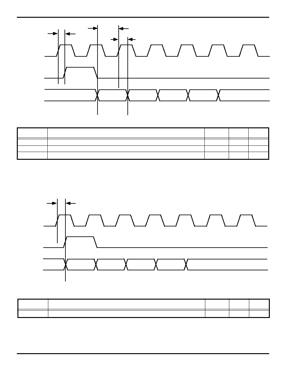
8.03
46
IDT77155
ADVANCED INFORMATION
155Mbps ATM PHY (TC-PMD) USER NETWORK INTERFACE
Commercial Temperature Range
RCLK
RGFC
RCP
GFC[3]
GFC[2]
GFC[1]
GFC[0]
X
X
3497 drw 17
t
RSO
TCLK
TGFC
TCP
GFC[3]
GFC[2]
GFC[1]
GFC[0]
X
X
3497 drw 16
t
GSO
t
GSU
t
GHD
Figure 13. Transmit GFC Serial Link Timing
Figure 14. Receive GFC Serial Link Timing
SYMBOL DISCRIPTION MIN. MAX. UNITS
tGHD
TGFC hold to TCLK
1
ns
tGSO
Transmit clock TCLK to TCP valid
2
15
ns
tGSU
TGFC set up to TCLK
10
ns
SYMBOL DISCRIPTION MIN. MAX. UNITS
tRSO
Receive clock RCLK to RCP/RGFC valid
2
15
ns

IIDT77155
ADVANCED INFORMATION
155Mbps ATM PHY (TC-PMD) USER NETWORK INTERFACE
Commercial Temperature Range
8.03
47
TXD+
TXD-
TXC+
TXC-
3497 drw 18
t
SOV
Figure 15. Line Interface Transmit Timing
Figure 16. Line Interface Receive Timing
SYMBOL DISCRIPTION MIN. MAX. UNITS
Receive line clock duty cycle
40%
60%
%
(155.52 MHz or 51.84 MHz - RBYP high)
( 19.44 MHz or 6.48 MHz - RBYP low )
tSOV
Transmit line clock output low to transmit differential data output
-2
2
ns
SYMBOL DISCRIPTION MIN. MAX. UNITS
Receive line clock duty cycle
40%
60%
%
(155.52 MHz or 51.84 MHz - RBYP high)
( 19.44 MHz or 6.48 MHz - RBYP low )
tRDHD
Receive data hold time (RBYP high)
1
ns
tRDSU
Receive data setup time (RBYP high)
2
ns
RXD+
RXD-
RRCLK+
RRCLK-
3497 drw 19
t
RDHD
t
RDSU
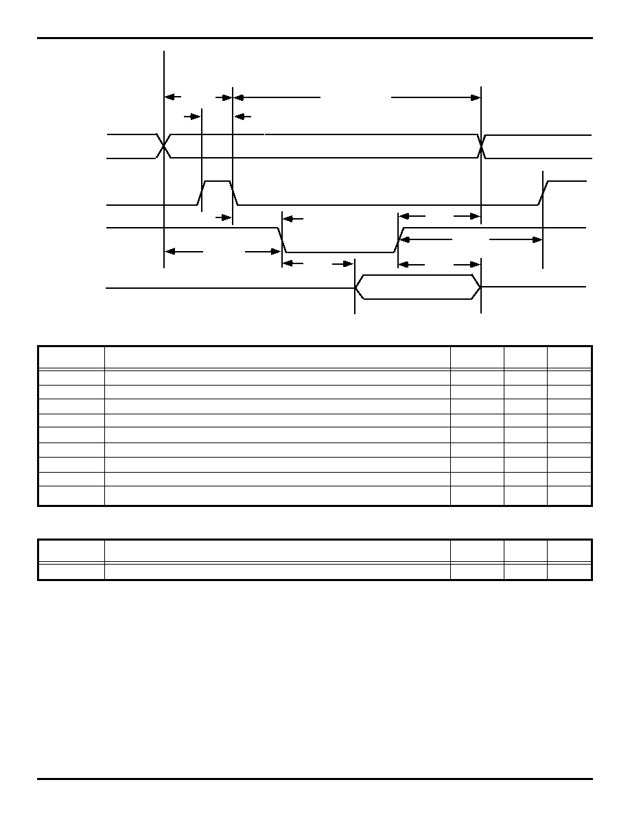
8.03
48
IDT77155
ADVANCED INFORMATION
155Mbps ATM PHY (TC-PMD) USER NETWORK INTERFACE
Commercial Temperature Range
ALE
D[7:0]
CS / RD
3497 drw 20
A[7:0]
X
X
Valid Address
t
LW
t
ALSU
t
ALHD
Valid Data
t
ARSU
t
RD
t
LRSU
t
ARHD
t
LRHD
t
DT
Figure 17. Microporcessor Read Timing
SYMBOL DISCRIPTION MIN. MAX. UNITS
tALHD
Address to latch enable hold time
10
ns
tALSU
Address to latch enable setup time
20
ns
tARHD
Address to read hold time
5
ns
tARSU
Address to read setup time
25
ns
tDT
Read to output data tristate
20
ns
tLRHD
Latch enable to read hold time
5
ns
tLRSU
Latch enable to read setup time
5
ns
tLW
Latch enable pulse width
20
ns
tRD
Valid read to data propagation delay
80
ns
SYMBOL DISCRIPTION MIN. MAX. UNITS
tBB
Time between consecutive operations
150
ns
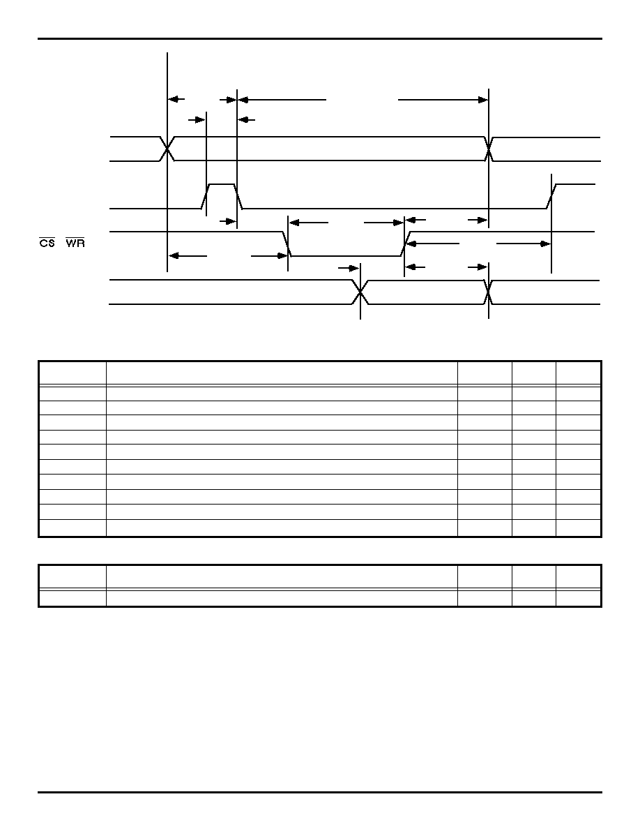
IIDT77155
ADVANCED INFORMATION
155Mbps ATM PHY (TC-PMD) USER NETWORK INTERFACE
Commercial Temperature Range
8.03
49
ALE
D[7:0]
/
X
X
3497 drw 21
A[7:0]
X
X
Valid Address
t
LW
t
ALSU
t
ALHD
Valid Data
t
AWSU
t
LWSU
t
AWHD
t
LWHD
t
DWHD
t
DWSU
t
WW
Figure 18. Microprocessor Write Timing
SYMBOL DISCRIPTION MIN. MAX. UNITS
tALHD
Address to latch enable hold time
10
ns
tALSU
Address to latch enable setup time
20
ns
tAWHD
Address to write hold time
5
ns
tAWSU
Address to write setup time
25
ns
tDWHD
Data to write hold time
1
ns
tDWSU
Data to write setup time
5
ns
tLW
Latch enable pulse width
20
ns
tLWHD
Latch enable to write hold time
5
ns
tLWSU
Latch enable to write setup time
5
ns
tWW
Write pulse width
40
ns
SYMBOL DISCRIPTION MIN. MAX. UNITS
tBB
Time between consecutive operations
150
ns

8.03
50
IDT77155
ADVANCED INFORMATION
155Mbps ATM PHY (TC-PMD) USER NETWORK INTERFACE
Commercial Temperature Range
ORDERING INFORMATION
ADVANCE INFORMATION DATASHEET: DEFINITION
"Advance Information" datasheets contain initial descriptions, subject to change, for products that are in development,
including features and block diagrams.
Datasheet Document History
1/10/96:
Initial Public Release
2/16/96:
Corrected Package Designator to PQF
4/9/96:
Revised Public Release
9/16/96:
Corrected block diagrams, made minor text clearifications.
11/26/95:
Added timing diagrams and corrected signals that are active low.
Integrated Device Technology, Inc.
2975 Stender Way, Santa Clara, CA 95054-3090
Telephone: (408) 727-6116
FAX 408-492-8674
Integrated Device Technology, Inc. reserves the right to make changes to the specifications in this data sheet in order to improve design or performance and to supply the best possible product.
Package
IDT
XXXXX
Device Type
A
Power
NNN
Speed
A
A
Process/
Temp. Range
Blank
155
Speed in Mb/s
77155
155Mb/s ATM PHY SONET/SDH
Framer with Clock Recovery User
Network Interface
Commercial
3497 drw 22
PX
128-pin Plastic Quad Flatpack
L
Low Power CMOS