COMMERCIAL TEMPERATURE RANGE
JUNE 2000
©1998 Integrated Device Technology, Inc.
DSC-5349/2
1
KEY FEATURES
∑ Full-duplex Segmentation and Reassembly (SAR) at
155 Mbps "wire-speed" (310 Mbps aggregate speed).
∑ Performs ATM layer protocol functions.
∑ Supports AAL5, AAL3/4, AAL0 and Raw Cell formats.
∑ Supports Constant Bit Rate (CBR), Variable Bit Rate
(VBR), and Unassigned Bit Rate (UBR), and Available Bit
Rate (ABR) service classes.
∑ Segments and reassembles CS-PDUs into host memory.
∑ Four buffer pools for independent or chained reassembly
∑ PCI 2.1 compliant.
∑ Operates with ATM networks up to 155.52 Mbps.
∑ Up to 256 active transmit connections.
∑ Up to 256 active receive connections.
∑ UTOPIA Level 1 Interface to PHY.
∑ Utility & Management Interface to PHY.
∑ Stand-alone controller: embedded processor not re-
quired.
∑ Supports high-performance, lowest-cost ATM NIC
solution.
∑ Supports any buffer alignment condition.
∑ Supports Big and Little Endian data transfers.
∑ Free Bufffer Queues mapped into PCI memory space.
∑ Configurable transmit FIFO depth for reduced latency.
∑ Null cell disable option during transmit.
∑ Supports greater local memory size.
∑ Large Rx FIFO size (configurable to 1024 Kbytes).
∑ Meets Power Management specification.
∑ Automatic AAL5 padding.
∑ UNI 3.1, TM 4.0 compliant.
∑ Pin compatible with IDT 77211 SAR
Integrated Device Technology, Inc.
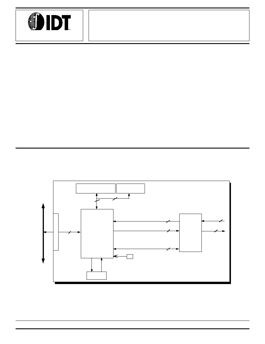
SYSTEM-LEVEL FUNCTIONAL BLOCK DIAGRAM
155 Mbps ATM SAR CONTROLLER
WITH ABR SUPPORT FOR PCI-BASED
NETWORKING APPLICATIONS
PRELIMINARY
INFORMATION
IDT77222
The IDT logo is a registered trademark of Integrated Device Technology, Inc.
32
33 M H Z
IDT77222
155Mbps
P C I A T M
ABR SAR
P H Y
Rx U TO PIA B us
Tx U TO P IA B us
U tility B u s
8
8
8
2
2
155M bps
1 6 K x 3 2
S R A M
EEPROM
32
80.0M HZ O S C.
PCI BUS
PROM
8
5349 drw 01
P
C
I
I
n
t
er
f
a
ce
IDT77222 155Mb/s ATM Segmentation & Reassembly (SAR) Controller
PRELIMINARY
with ABR for the PCI Local Bus
COMMERCIAL TEMPERATURE RANGE
2
.
/
8
P C I
In terface
PCI Bus
T ra nsm it
C o n tro l
T x
U to p ia
In terface
S R A M IN T E R F A C E
R eceive
C o n tro l
R x
U top ia
Interface
T x U to p ia
Bus
S R A M
Bus
R x U to p ia
Bus
U tilit y
E E P R O M O U T
5 3 4 9 d rw 0 2
/
32
E E P R O M IN
/
8
/
8
/
32
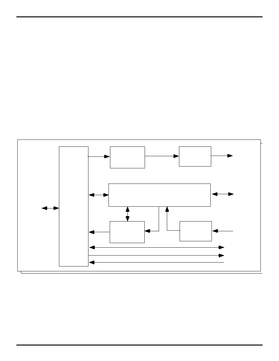
Block Diagram of the IDT77222
DESCRIPTION
The IDT77222 is a member of IDT's family of SAR products
for Asynchronous Transfer Mode (ATM) networks. The
IDT77222 performs both the ATM Adaptation Layer (AAL)
Segmentation and Reassembly (SAR) function and the ATM
layer protocol functions.
A Network Interface Card (NIC) or internetworking product
based on the IDT77222 uses host memory, rather than local
memory, to reassemble Convergence Sublayer Protocol Data
Units (CS-PDUs) from ATM cell payloads received from the
network. When transmitting, as CS-PDUs become ready,
they are queued in host memory and segmented by the
IDT77222 into ATM cell payloads. From this, the IDT77222
then creates complete 53-byte ATM cells which are sent
through the network. The IDT77222's on-chip PCI bus master
interface provides efficient, low latency DMA transfers with the
host system, while its UTOPIA interface provides direct con-
nection to PHY components used in 25.6 Mbps to 155 Mbps
ATM networks.
The IDT77222 is fabricated using state-of-the-art CMOS
technology, providing the highest levels of integration, perfor-
mance and reliability, with the low-power consumption char-
acteristics of CMOS.
IDT77222 155Mb/s ATM Segmentation & Reassembly (SAR) Controller
PRELIMINARY
with ABR for the PCI Local Bus
COMMERCIAL TEMPERATURE RANGE
3
PACKAGE PINOUT
1
Vcc
2
AD(31)
3
AD(30)
4
AD(29)
5
AD(28)
6
AD(27)
7
AD(26)
8
GND
9
GND
10
AD(25)
11
AD(24)
12
C/BE(3)
13
IDSEL
14
AD(23)
15
AD(22)
16
GND
17
GND
18
AD(21)
19
Vcc
20
AD(20)
21
AD(19)
22
AD(18)
23
AD(17)
24
AD(16)
25
GND
26
GND
27
C/BE(2)
28
Vcc
29
FRAME
30
IRDY
31
TRDY
32
DEVSEL
33
STOP
34
GND
35
GND
36
INTA
37
Vcc
38
PERR
39
SERR
40
PAR
41
C/BE(1)
42
AD(15)
43
GND
44
GND
45
AD(14)
46
AD(13)
47
AD(12)
48
AD(11)
49
AD(10)
50
AD(9)
51
AD(8)
52
GND
156
155
154
153
152
151
150
149
148
147
146
145
144
143
142
141
140
139
138
137
136
135
134
133
132
131
130
129
128
127
126
125
124
123
122
121
120
119
118
117
116
115
114
113
112
111
110
109
108
107
106
105
GND
PHY_INT
PHY_RST
UTL_ALE
UTL_RD
UTL_WR
GND
UTL_AD(7)
UTL_AD(6)
UTL_AD(5)
UTL_AD(4)
Vcc
UTL_AD(3)
GND
UTL_AD(2)
UTL_AD(1)
UTL_AD(0)
Vcc
SAR_CLK
GND
SR_I/O(30)
SR_I/O(29)
GND
SR_I/O(28)
SR_I/O(27)
SR_I/O(26)
SR_I/O(25)
SR_I/O(24)
Vcc
SR_I/O(23)
GND
SR_I/O(22)
SR_I/O(21)
EEDO
EEDI
EESCLK
EECS
Vcc
E_CE
SR_I/O(31)
SR_I/O(20)
SR_I/O(19)
SR_I/O(18)
SR_I/O(17)
GND
SR_I/O(16)
SR_I/O(15)
SR_I/O(14)
SR_I/O(13)
SR_I/O(12)
SR_I/O(11)
Vcc
5
3
5
4
5
5
5
6
5
7
5
8
5
9
6
0
6
1
6
2
6
3
6
4
6
5
6
6
6
7
6
8
6
9
7
0
7
1
7
2
7
3
7
4
7
5
7
6
7
7
7
8
7
9
8
0
8
1
8
2
8
3
8
4
8
5
8
6
8
7
8
8
8
9
9
0
9
1
9
2
9
3
9
4
9
5
9
6
9
7
9
8
9
9
1
0
0
1
0
1
1
0
2
1
0
3
1
0
4
V
c
c
G
N
D
C
/
B
E
(
0
)
A
D
(
7
)
V
c
c
A
D
(
6
)
A
D
(
5
)
A
D
(
4
)
G
N
D
G
N
D
A
D
(
3
)
A
D
(
2
)
A
D
(
1
)
A
D
(
0
)
G
N
D
N
/
C
S
R
_
WE
S
R
_
A
1
3
S
R
_
A
8
S
R
_
A
9
S
R
_
A
1
1
S
R
_
O
E
S
R
_
A
1
0
S
R
_
C
S
N
/
C
G
N
D
N
/
C
V
c
c
S
R
_
A
1
2
S
R
_
A
7
S
R
_
A
6
S
R
_
A
5
S
R
_
A
4
S
R
_
A
3
S
R
_
A
2
S
R
_
A
1
S
R
_
A
0
G
N
D
G
N
D
S
R
_
I
/
O
(
0
)
S
R
_
I
/
O
(
1
)
S
R
_
I
/
O
(
2
)
S
R
_
I
/
O
(
3
)
S
R
_
I
/
O
(
4
)
S
R
_
I
/
O
(
5
)
S
R
_
I
/
O
(
6
)
G
N
D
S
R
_
I
/
O
(
7
)
S
R
_
I
/
O
(
8
)
S
R
_
I
/
O
(
9
)
S
R
_
I
/
O
(
1
0
)
G
N
D
208 2
0
7
2
0
6
2
0
5
2
0
4
2
0
3
2
0
2
2
0
1
2
0
0
1
9
9
1
9
8
1
9
7
1
9
6
1
9
5
1
9
4
1
9
3
1
9
2
1
9
1
1
6
1
1
9
0
1
8
9
1
8
8
1
8
7
1
8
6
1
8
5
1
8
4
1
8
3
1
8
2
1
8
1
1
8
0
1
7
9
1
7
8
1
7
7
1
7
6
1
7
5
1
7
4
1
7
3
1
7
2
1
7
1
1
7
0
1
6
9
1
6
8
1
6
7
1
6
6
1
6
5
1
6
4
1
6
3
1
6
2
1
6
0
1
5
9
1
5
8
1
5
7
G
N
D
V
c
c
R
E
Q
G
N
T
C
L
K
R
S
T
G
N
D
G
N
D
G
N
D
V
c
c
V
c
c
G
N
D
G
N
D
T
X
P
A
R
I
T
Y
P
H
Y
_
C
L
K
R
X
C
L
K
G
N
D
R
X
E
M
P
T
Y
/
R
x
C
L
A
V
R
X
E
N
B
R
X
D
A
T
A
(
7
)
R
X
D
A
T
A
(
6
)
R
X
D
A
T
A
(
5
)
R
X
D
A
T
A
(
4
)
G
N
D
R
X
D
A
T
A
(
3
)
R
X
D
A
T
A
(
2
)
R
X
D
A
T
A
(
1
)
R
X
D
A
T
A
(
0
)
G
N
D
T
X
C
L
K
T
X
F
U
L
L
/
T
x
C
L
A
V
T
X
E
N
B
T
X
S
O
C
G
N
D
T
X
D
A
T
A
(
7
)
T
X
D
A
T
A
(
6
)
V
C
C
T
X
D
A
T
A
(
5
)
T
X
D
A
T
A
(
4
)
G
N
D
T
X
D
A
T
A
(
3
)
T
X
D
A
T
A
(
2
)
T
X
D
A
T
A
(
1
)
T
X
D
A
T
A
(
0
)
U
T
L
_
C
S
(
1
)
U
T
L
_
C
S
(
0
)
V
c
c
Index
5349 drw 03
R
X
S
O
C
N
A
N
D
_E
N
C
LK
_O
U
T
G
N
D
N
A
N
D
_O
U
T
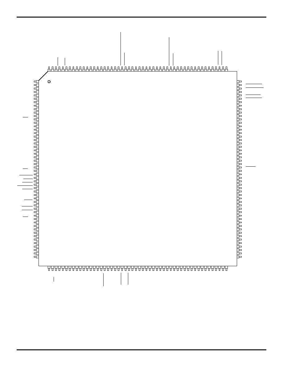
IDT77222 SAR Controller
With ABR Support
208 Pin PQFP
Pinout
PU-208
Refer to PSC-4053 for
detailed package drawing
IDT77222 155Mb/s ATM Segmentation & Reassembly (SAR) Controller
PRELIMINARY
with ABR for the PCI Local Bus
COMMERCIAL TEMPERATURE RANGE
4
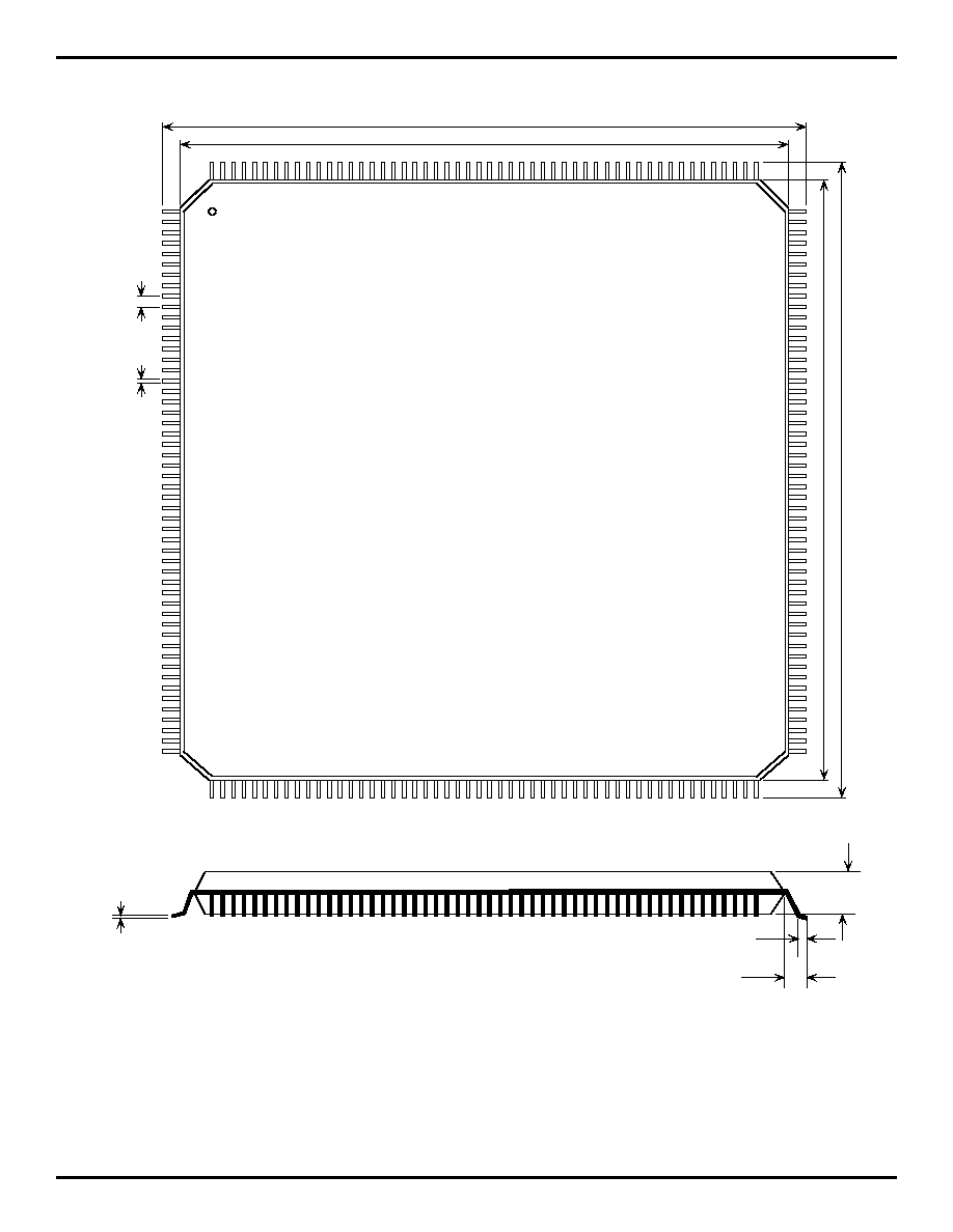
PACKAGE DRAWING
1
52
156
105
53
104
208
157
Index
1.228 ±0.016 (31.2 ±0.4)
1.10 ±0.004 (28.0 ±0.1)
1
.
228
±0
.0
16
(3
1.
2
±
0
.4
)
1.
1
0
±
0
.0
04
(28.
0
±0
.1
)
0.02 ±0.004
(0.5 ±0.1)
0.008 ±0.004
(0.2 ±0.1)
0.024 ±0.008
(0.6 ±0.2)
0.063 (1.6)
0.013 ±0.002
(0.33 ±0.06)
0.133 ±0.004
(3.37 ±0.1)
5349 drw 04

IDT77222 155Mb/s ATM Segmentation & Reassembly (SAR) Controller
PRELIMINARY
with ABR for the PCI Local Bus
COMMERCIAL TEMPERATURE RANGE
5
PIN DEFINITIONS
Pin #
Name
I/O
Bus Name
Description
1
V
CC
I
power
2
AD(31)
I/O
PCI
address/data line
3
AD(30)
I/O
PCI
address/data line
4
AD(29)
I/O
PCI
address/data line
5
AD(28)
I/O
PCI
address/data line
6
AD(27)
I/O
PCI
address/data line
7
AD(26)
I/O
PCI
address/data line
8
GND
I
power
9
GND
I
power
10
AD(25)
I/O
PCI
address/data line
11
AD(24)
I/O
PCI
address/data line
12
C/BE(3)
I/O
PCI
bus command
13
IDSEL
I
PCI
bus ID select
14
AD(23)
I/O
PCI
address/data line
15
AD(22)
I/O
PCI
address/data line
16
GND
I
power
17
GND
I
power
18
AD(21)
I/O
PCI
address/data line
19
V
CC
I
power
20
AD(20)
I/O
PCI
address/data line
21
AD(19)
I/O
PCI
address/data line
22
AD(18)
I/O
PCI
address/data line
23
AD(17)
I/O
PCI
address/data line
24
AD(16)
I/O
PCI
address/data line
25
GND
I
power
26
GND
I
power
27
C/BE(2)
I/O
PCI
bus command
28
V
CC
I
power
29
Frame
I/O
PCI
cycle frame
30
IRDY
I/O
PCI
initiator ready
31
TRDY
I/O
PCI
target ready
32
DEVSEL
I/O
PCI
target indicating address decode
33
STOP
I/O
PCI
target requesting master to stop
34
GND
I
power
35
GND
I
power
36
INTA
O
PCI
"interrupt" "A" "request"
37
V
CC
I
power
38
PERR
I/O
PCI
data parity error
39
SERR
O
PCI
system error
40
PAR
I/O
PCI
parity (for AD[0:31] and C/BE[0:3])
41
C/BE(1)
I/O
PCI
bus command
42
AD(15)
I/O
PCI
address/data line
43
GND
I
power
44
GND
I
power
45
AD(14)
I/O
PCI
address/data line
46
AD(13)
I/O
PCI
address/data line
47
AD(12)
I/O
PCI
address/data line
48
AD(11)
I/O
PCI
address/data line
5349 tbl 01

IDT77222 155Mb/s ATM Segmentation & Reassembly (SAR) Controller
PRELIMINARY
with ABR for the PCI Local Bus
COMMERCIAL TEMPERATURE RANGE
6
PIN DEFINITIONS (CON'T.)
Pin #
Name
I/O
Bus Name
Description
49
AD(10)
I/O
PCI
address/data line
50
AD(9)
I/O
PCI
address/data line
51
AD(8)
I/O
PCI
address/data line
52
GND
I
power
53
V
CC
I
power
54
GND
I
power
55
C/
BE
(0)
I/O
PCI
bus command
56
AD(7)
I/O
PCI
address/data line
57
V
CC
I
power
58
AD(6)
I/O
PCI
address/data line
59
AD(5)
I/O
PCI
address/data line
60
AD(4)
I/O
PCI
address/data line
61
GND
I
power
62
GND
I
power
63
AD(3)
I/O
PCI
address/data line
64
AD(2)
I/O
PCI
address/data line
65
AD(1)
I/O
PCI
address/data line
66
AD(0)
I/O
PCI
address/data line
67
GND
I
power
68
N/C
No connect
69
SR_WE
O
SRAM
Write enable
70
SR_A13
O
SRAM
Address line
71
SR_A8
O
SRAM
Address line
72
SR_A9
O
SRAM
Address line
73
SR_A11
O
SRAM
Address line
74
SR_OE
O
SRAM
Output Enable control
75
SR_A10
O
SRAM
Address line
76
SR_CS
O
SRAM
Chip Select
77
N/C
No connect
78
GND
I
power
79
N/C
No connect
80
V
CC
I
power
81
SR_A12
O
SRAM
Address line
82
SR_A7
O
SRAM
Address line
83
SR_A6
O
SRAM
Address line
84
SR_A5
O
SRAM
Address line
85
SR_A4
O
SRAM
Address line
86
SR_A3
O
SRAM
Address line
87
SR_A2
O
SRAM
Address line
88
SR_A1
O
SRAM
Address line
89
SR_A0
O
SRAM
Address line
90
GND
I
power
91
GND
I
power
92
SR_I/O(0)
I/O
SRAM
Data input/output line
93
SR_I/O(1)
I/O
SRAM
Data input/output line
94
SR_I/O(2)
I/O
SRAM
Data input/output line
95
SR_I/O(3)
I/O
SRAM
Data input/output line
96
SR_I/O(4)
I/O
SRAM
Data input/output line
5349 tbl 02

IDT77222 155Mb/s ATM Segmentation & Reassembly (SAR) Controller
PRELIMINARY
with ABR for the PCI Local Bus
COMMERCIAL TEMPERATURE RANGE
7
PIN DEFINITIONS (CON'T.)
Pin #
Name
I/O
Bus Name
Description
97
SR_I/O(5)
I/O
SRAM
Data input/output line
98
GND
I
power
99
SR_I/O(6)
I/O
SRAM
Data input/output line
100
SR_I/O(7)
I/O
SRAM
Data input/output line
101
SR_I/O(8)
I/O
SRAM
Data input/output line
102
SR_I/O(9)
I/O
SRAM
Data input/output line
103
SR_I/O(10)
I/O
SRAM
Data input/output line
104
GND
I
power
105
V
CC
I
power
106
SR_I/O(11)
I/O
SRAM
Data input/output line
107
SR_I/O(12)
I/O
SRAM
Data input/output line
108
SR_I/O(13)
I/O
SRAM
Data input/output line
109
SR_I/O(14)
I/O
SRAM
Data input/output line
110
SR_I/O(15)
I/O
SRAM
Data input/output line
111
SR_I/O(16)
I/O
SRAM
Data input/output line
112
GND
I
power
113
SR_I/O(17)
I/O
SRAM
Data input/output line
114
SR_I/O(18)
I/O
SRAM
Data input/output line
115
SR_I/O(19)
I/O
SRAM
Data input/output line
116
SR_I/O(20)
I/O
SRAM
Data input/output line
117
SR_I/O(21)
I/O
SRAM
Data input/output line
118
SR_I/O(22)
I/O
SRAM
Data input/output line
119
GND
I
power
120
SR_I/O(23)
I/O
SRAM
Data input/output line
121
V
CC
I
power
122
SR_I/O(24)
I/O
SRAM
Data input/output line
123
SR_I/O(25)
I/O
SRAM
Data input/output line
124
SR_I/O(26)
I/O
SRAM
Data input/output line
125
SR_I/O(27)
I/O
SRAM
Data input/output line
126
SR_I/O(28)
I/O
SRAM
Data input/output line
127
GND
I
power
128
SR_I/O(29)
I/O
SRAM
Data input/output line
129
SR_I/O(30)
I/O
SRAM
Data input/output line
130
SR_1/O(31)
I/O
SRAM
Data input/output line
131
E_CE
O
EPROM
EPROM chip select
132
V
CC
I
power
133
EECS
O
EEPROM
chip select
134
EESCLK
O
EEPROM
clock
135
EEDI
I
EEPROM
Data input
136
EEDO
O
EEPROM
Data output
137
GND
I
power
138
SAR_CLK
I
SAR clock input
139
V
CC
I
power
140
UTL_AD(0)
I/O
Utility
address/data bus
141
UTL_AD(1)
I/O
Utility
address/data bus
142
UTL_AD(2)
I/O
Utility
address/data bus
143
GND
I
power
144
UTL_AD(3)
I/O
Utility
address/data bus
5349 tbl 03

IDT77222 155Mb/s ATM Segmentation & Reassembly (SAR) Controller
PRELIMINARY
with ABR for the PCI Local Bus
COMMERCIAL TEMPERATURE RANGE
8
PIN DEFINITIONS (CON'T.)
Pin #
Name
I/O
Bus Name
Description
145
V
CC
I
power
146
UTL_AD(4)
I/O
Utility
address/data bus
147
UTL_AD(5)
I/O
Utility
address/data bus
148
UTL_AD(6)
I/O
Utility
address/data bus
149
UTL_AD(7)
I/O
Utility
address/data bus
150
GND
I
power
151
UTL_WR
O
Utility
write control
152
UTL_RD
O
Utility
read control
153
UTL_ALE
O
Utility
address latch enable
154
PHY_RST
O
PHY
rest control
155
PHY_INT
I
PHY
interrupt input from PHY
156
GND
I
power
157
V
CC
I
power
158
UTL_CS(0)
O
Utility
chip select (0)
159
UTL_CS(1)
O
Utility
chip select (1)
160
TxData(0)
O
UTOPIA
transmit data bit 0
161
TxData(1)
O
UTOPIA
transmit data bit 1
162
TxData(2)
O
UTOPIA
transmit data bit 2
163
TxData(3)
O
UTOPIA
transmit data bit 3
164
GND
I
power
165
TxData(4)
O
UTOPIA
transmit data bit 4
166
TxData(5)
O
UTOPIA
transmit data bit 5
167
V
CC
I
power
168
TxData(6)
O
UTOPIA
transmit data bit 6
169
TxData(7)
O
UTOPIA
transmit data bit 7
170
GND
I
power
171
TxSOC
O
UTOPIA
transmit start of cell
172
TxEnb
O
UTOPIA
transmit enable control
173
TxFull
/TxCLAV
I
UTOPIA
transmit buffer full
174
TxCLK
O
UTOPIA
transmit data sync clock
175
GND
I
power
176
RxData(0)
I
UTOPIA
receive data bit 0
177
RxData(1)
I
UTOPIA
receive data bit 1
178
RxData(2)
I
UTOPIA
receive data bit 2
179
RxData(3)
I
UTOPIA
receive data bit 3
180
GND
I
power
181
RxData(4)
I
UTOPIA
receive data bit 4
182
RxData(5)
I
UTOPIA
receive data bit 5
183
RxData(6)
I
UTOPIA
receive data bit 6
184
RxData(7)
I
UTOPIA
receive data bit 7
185
RxSOC
I
UTOPIA
receive start of cell
186
RxEnb
O
UTOPIA
receive enable control
187
RxEmpty
/RxCLAV
I
UTOPIA
receive buffer empty
188
GND
I
power
189
RxClk
O
UTOPIA
receive data sync clock
190
PHY_Clk
I
UTOPIA
Transmit sync clock input
191
TxParity
O
UTOPIA
transmit data parity bit
192
GND
I
power
5349 tbl 04

IDT77222 155Mb/s ATM Segmentation & Reassembly (SAR) Controller
PRELIMINARY
with ABR for the PCI Local Bus
COMMERCIAL TEMPERATURE RANGE
9
PIN DEFINITIONS (CON'T.)
Pin #
Name
I/O
Bus Name
Description
193
NAND_OUT
O
power
NAND output chain
194
GND
I
power
195
GND
I
power
196
V
CC
I
power
197
V
CC
I
power
198
CLK_OUT
O
power
SAR_Clk divided by 3
199
GND
I
power
200
GND
I
power
201
NAND_EN
I
power
NAND input chain
202
GND
I
power
203
RST
I
PCI
system bus reset
204
CLK
I
PCI
bus clock
205
GNT
I
PCI
bus grant signal from arbiter
206
REQ
O
PCI
bus request
207
V
CC
I
power
208
GND
I
power
5349 tbl 05

IDT77222 155Mb/s ATM Segmentation & Reassembly (SAR) Controller
PRELIMINARY
with ABR for the PCI Local Bus
COMMERCIAL TEMPERATURE RANGE
10
ABSOLUTE MAXIMUM RATINGS
RECOMMENDED OPERATING CONDITIONS
Symbol
Parameter
Min.
Max.
Unit
V
CC
Supply Voltage
-0.3
6.5
V
V
IN
Input Voltage
V
SS
- 0.3
V
CC
+ 0.3
V
V
OUT
Output Voltage
V
SS
- 0.3
V
CC
+ 0.3
V
T
stg
Storage Temperature
-55
125
deg.C
5349 tbl 06
CLOCKING
Symbol
Parameter
Min.
Max.
Unit
V
CC
Supply Voltage
4.75
5.25
V
V
I
Input Voltage
0
V
CC
V
T
A
Operating temperature
0
70
deg.C
titr
Input TTL rise time
____
2
ns
titf
Input TTL rall time
____
2
ns
5349 tbl 07
CAPACITANCE
Symbol
Parameter
Rate
Min.
Max.
Unit
SAR_CLK
SAR clock input freq.
155Mb/s
77
80
MHz
25Mb/s
25
80
MHz
PHY_CLK
PHY clock input freq.
155Mb/s
19.44
40
MHz
25Mb/s
3
40
MHz
PCI_CLK
PCI clock input freq.
33MHz
0
33.3
MHz
5349 tbl 08
Symbol
Parameter
Condition
Min.
Max.
Typical
Unit
C
IN
Input Capacitance
except PCI Bus
____
____
4
pF
C
OUT
Output Capacitance
all outputs
____
____
6
pF
C
bid
Bi-Directional Capacitance
all bi-directional pins
____
____
10
pF
C
inpci
PCI Bus Input Capacitance
PCI Bus inputs
____
10
____
pF
C
clkpci
PCI Bus Clock Input Capacitance
____
5
12
____
pF
C
idsel
PCI Bus ID Select Input Capacitance
____
____
8
____
pF
5349 tbl 09

IDT77222 155Mb/s ATM Segmentation & Reassembly (SAR) Controller
PRELIMINARY
with ABR for the PCI Local Bus
COMMERCIAL TEMPERATURE RANGE
11
DC OPERATING CONDITIONS
Symbol
Parameter
Condition
Min.
Max.
Typical
Unit
Vil
Low-level TTL input voltage
____
-0.7V
0.8
____
V
Vih
High-level TTL input voltage
____
2
V
CC
+ 0.2V
____
V
Vol
Low-level TTL output voltage
except PCI Bus
____
0.4
____
V
Vol
PCI Bus Low-level TTL output voltage
PCI Bus voltage
____
0.55
____
V
Voh
High-level TTL output voltage
____
2.4
____
____
V
Iol
Low-level TTL output current:
SR_A(18-0)
V
SS
+ 0.4V
12
____
____
mA
Ioh
High-level TTL output current:
SR_A(18-0)
2.4V
-4
____
____
mA
Iol
Low-level TTL output current:
RxEnb
, RxClk, TxSOC,
TxData (7-0),
TxEnb
, TxParity,
TxClk,
WE
,
OE
,
CS
,
SR_D31-0
V
SS
+ 0.4V
6
____
____
mA
Ioh
High-level TTL output current:
RxEnb
, RxClk, TxSoc,
TxData7-0,
TxEnb
, TxParity,
TxClk,
SR_WE
,
SR
,
OE
,
SR_CS
,
SR_I/O(31-0)
2.4V
-2
____
____
mA
Iol
Low-level TTL output current:
UTL_AD(7-0),
UTL_RD
,
UTL_WR
,
UTL_ALE
,
UTL_CS0/1
, EESCLK, EECS,
EEDO,
PHY_RST
V
SS
+ 0.4V
3
____
____
mA
Ioh
High-level TTL output current:
UTL_AD(7-0),
UTL_RD
,
UTL_WR
, UTL_ALE,
UTL_CS0/1
, EESCLK, EECS,
EEDO,
PHY_RST
2.4V
-1
____
____
mA
Iil
Input leakage current
V
SS
< V
IN
< Vdd
-1
1
____
uA
Ityp
Dynamic Supply Current
____
____
300
250
mA
5349 tbl 10
IDT77222 155Mb/s ATM Segmentation & Reassembly (SAR) Controller
PRELIMINARY
with ABR for the PCI Local Bus
COMMERCIAL TEMPERATURE RANGE
12
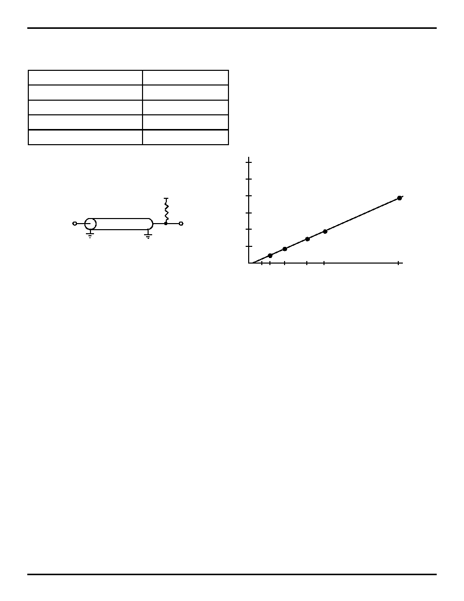
AC OPERATING CONDITIONS
AC TEST CONDITIONS
Input Pulse Levels
0 to 3.0V
Input Rise/Fall Times
2ns
Input Timing Ref. Level
1.5V
Output Ref. Level
1.5V
AC Test Load
See Figure Below
5349 tbl 11
1.5V
50
I/O
Z
0
= 50
1
2
3
4
20 30 50
100
200
tCD
(Typical, ns)
Capacitance (pF)
80
5
6
5349 drw 05
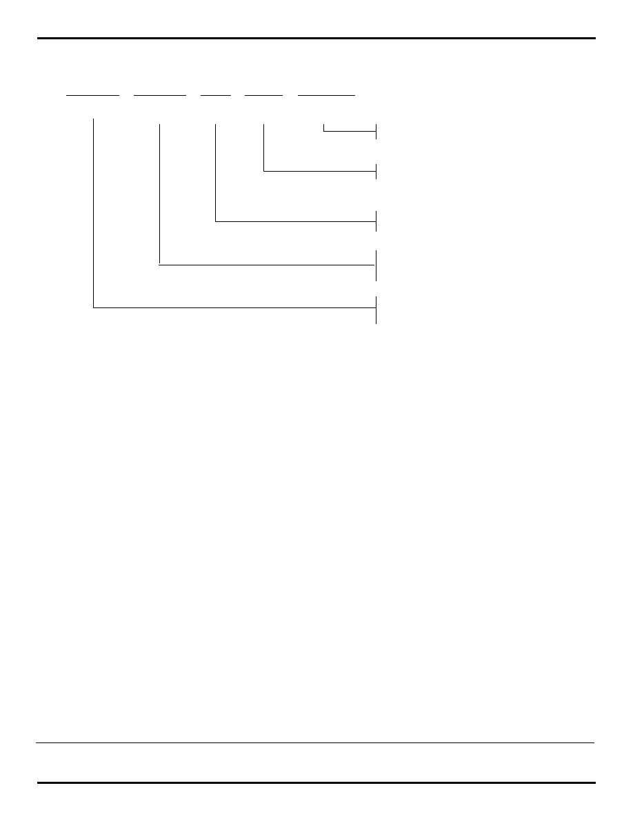
NAND TREE
The NAND Chain provides a simple test to verify that all bond wires are installed correctly and that all pads are correctly
soldered on a PCB.
All signal pads are linked in a NAND chain, which is enabled by asserting a high, or "1", on NAND_EN (pin 201). Asserting
a "1" on the other inputs forces NAND_OUT (pin 193) to "1". By successively setting the inputs to "0", starting at CLK_OUT
(pin 198) and moving to TXPARITY (pin 191), NAND_OUT will toggle with each change.
1. Apply a "1" to NAND_EN.
2. Set all the I/O's in the chain to "0" and NAND_OUT should be a "1".The connection order of the pins in the chain are
shown in the NAND Tree Pin Order table located on the following page.
3. Set CLK_OUT to a "0" and the NAND_OUT should be a "0".
4. Leaving pin 198 at a "1" set
RST
(pin 203) to "1" and NAND_OUT should be a "1".
5. Repeat for all remaining I/O's in the NAND chain.

IDT77222 155Mb/s ATM Segmentation & Reassembly (SAR) Controller
PRELIMINARY
with ABR for the PCI Local Bus
COMMERCIAL TEMPERATURE RANGE
13
Signal Name
Pin
Num ber
Signal Name
Pin
Num ber
Signal Name
Pin
Num ber
Signal Name
Pin
Num ber
C L K _ O UT
1 9 8
A D [1 2 ]
4 7
S R _I/O [0 6 ]
9 9
UT L _ A D [5 ]
1 4 7
RST
2 0 3
A D [11 ]
4 8
S R _I/O [0 7 ]
1 0 0
UT L _ A D [6 ]
1 4 8
C L K
2 0 4
A D [1 0 ]
4 9
S R _I/O [0 8 ]
1 0 1
UT L _ A D [7 ]
1 4 9
GNT
2 0 5
A D [9 ]
5 0
S R _I/O [0 9 ]
1 0 2
UTL_WR
1 5 1
REQ
2 0 6
A D [8 ]
5 1
S R _I/O [1 0 ]
1 0 3
UTL_RD
1 5 2
A D [3 1 ]
2
C /
BE
[0 ]
5 5
S R _ I/O [11]
1 0 6
UT L _ A L E
1 5 3
A D [3 0 ]
3
A D [7 ]
5 6
S R _I/O [1 2 ]
1 0 7
PHY_RST
1 5 4
A D [2 9 ]
4
A D [6 ]
5 8
S R _I/O [1 3 ]
1 0 8
PHY_INT
1 5 5
A D [2 8 ]
5
A D [5 ]
5 9
S R _I/O [1 4 ]
1 0 9
UTL_CS[0]
1 5 8
A D [2 7 ]
6
A D [4 ]
6 0
S R _I/O [1 5 ]
110
UTL_CS[1]
1 5 9
A D [2 6 ]
7
A D [3 ]
6 3
S R _I/O [1 6 ]
111
T xD ata[0]
1 6 0
A D [2 5 ]
1 0
A D [2 ]
6 4
S R _I/O [1 7 ]
113
T xD ata[1]
1 6 1
A D [2 4 ]
11
A D [1 ]
6 5
S R _I/O [1 8 ]
114
T xD ata[2]
1 6 2
C /
BE
[3 ]
1 2
A D [0 ]
6 6
S R _I/O [1 9 ]
115
T xD ata[3]
1 6 3
IDSEL
1 3
SR_WE
6 9
S R _I/O [2 0 ]
116
T xD ata[4]
1 6 5
A D [2 3 ]
1 4
S R _ A [1 3 ]
7 0
S R _I/O [2 1 ]
117
T xD ata[5]
1 6 6
A D [2 2 ]
1 5
S R _ A [8 ]
7 1
S R _I/O [2 2 ]
118
T xD ata[6]
1 6 8
A D [2 1 ]
1 8
S R _ A [9 ]
7 2
S R _I/O [2 3 ]
1 2 0
T xD ata[7]
1 6 9
A D [2 0 ]
2 0
S R _ A [11 ]
7 3
S R _I/O [2 4 ]
1 2 2
T xS O C
1 7 1
A D [1 9 ]
2 1
S R _ O E
7 4
S R _I/O [2 5 ]
1 2 3
TxEnb
1 7 2
A D [1 8 ]
2 2
S R _ A [1 0 ]
7 5
S R _I/O [2 6 ]
1 2 4
T xC L AV
1 7 3
A D [1 7 ]
2 3
SR_CS
7 6
S R _I/O [2 7 ]
1 2 5
T xC LK
1 7 4
A D [1 6 ]
2 4
S R _ A [1 2 ]
8 1
S R _I/O [2 8 ]
1 2 6
R xD a ta [0]
1 7 6
C /
BE
[2 ]
2 7
S R _ A [7 ]
8 2
S R _I/O [2 9 ]
1 2 8
R xD a ta [1]
1 7 7
Frame
2 9
S R _ A [6 ]
8 3
S R _I/O [3 0 ]
1 2 9
R xD a ta [2]
1 7 8
IRDY
3 0
S R _ A [5 ]
8 4
S R _I/O [3 1 ]
1 3 0
R xD a ta [3]
1 7 9
TRDY
3 1
S R _ A [4 ]
8 5
E_CE
1 3 1
R xD a ta [4]
1 8 1
DEVSEL
3 2
S R _ A [3 ]
8 6
E E C S
1 3 3
R xD a ta [5]
1 8 2
STOP
3 3
S R _ A [2 ]
8 7
E E S C LK
1 3 4
R xD a ta [6]
1 8 3
INITA
3 6
S R _ A [1 ]
8 8
E E D I
1 3 5
R xD a ta [7]
1 8 4
PERR
3 8
S R _ A [0 ]
8 9
E E D O
1 3 6
R xS O C
1 8 5
SERR
3 9
S R _I/O [0 0 ]
9 2
S A R _C LK
1 3 8
RxEnb
1 8 6
PA R
4 0
S R _I/O [0 1 ]
9 3
UT L _ A D [0 ]
1 4 0
R xC L AV
1 8 7
C /
BE
[1 ]
4 1
S R _I/O [0 2 ]
9 4
UT L _ A D [1 ]
1 4 1
R xC L K
1 8 9
A D [1 5 ]
4 2
S R _I/O [0 3 ]
9 5
UT L _ A D [2 ]
1 4 2
P HY _C LK
1 9 0
A D [1 4 ]
4 5
S R _I/O [0 4 ]
9 6
UT L _ A D [3 ]
1 4 4
T xP a rity
1 9 1
A D [1 3 ]
4 6
S R _I/O [0 5 ]
9 7
UT L _ A D [4 ]
1 4 6
53 49 tbl 12
NAND TREE PIN OREDER

IDT77222 155Mb/s ATM Segmentation & Reassembly (SAR) Controller
PRELIMINARY
with ABR for the PCI Local Bus
COMMERCIAL TEMPERATURE RANGE
14
Symbol
Parameter
Min.
Max.
Unit
tval
CLK to Output Signal Valid Delay: AD31-0, C/
BE
3-0, PAR,
FRAME
,
IRDY
,
DEVSEL
,
TRDY
,
STOP
,
PERR
,
SERR
2
11
ns
tval(ptp)
CLK to Output Signal Valid Delay:
REQ
2
12
ns
ton
Float to Signal Active Delay: AD31-0, C/
BE
3-0, PAR,
FRAME
,
IRDY
,
DEVSEL
,
TRDY
,
STOP
,
PERR
,
SERR
2
____
ns
toff
Signal Active to Float Delay: AD31-0, C/
BE
3-0, PAR,
FRAME
,
IRDY
,
DEVSEL
,
TRDY
,
STOP
,
PERR
,
SERR
____
28
ns
tsu
Input Setup Time to CL
K :
AD31-0, C/
BE
3-0, PAR,
FRAME
,
IRDY
,
DEVSEL
,
TRDY
,
STOP
,
PERR
7
____
ns
tsu(ptp)
Input Setup Time to CLK:
GNT
, (
REQ
)
10(12)
____
ns
th
Input Hold Time from CLK: AD31-0, C/
BE
3-0, PAR,
FRAME
,
IRDY
,
DEVSEL
,
TRDY
,
STOP
,
PERR
,
GNT
2 *
____
ns
trst-pwr
Reset Active Time After Power Stable
1
____
ns
trst-clk
Reset Active Time After CLK Stable
100
____
ns
trst-off
Reset Active to Output Float Delay: AD31-0, C/
BE
3-0, PAR,
FRAME
,
IRDY
,
DEVSEL
,
TRDY
,
STOP
,
PERR
,
SERR
____
40
ns
thigh
Clock high time
11n
____
ns
tlow
Clock low time
11n
____
ns
5349 tbl 13
* - Does not meet PCI Local Bus revision 2.1 timing specification
PCI BUS (SEE FIGURE 1& 2)

IDT77222 155Mb/s ATM Segmentation & Reassembly (SAR) Controller
PRELIMINARY
with ABR for the PCI Local Bus
COMMERCIAL TEMPERATURE RANGE
15
UTOPIA BUS (SEE FIGURE 3)
S ym b ol
P aram eter
M in.
M ax.
U nit
t1
T xC lk , R xC lk D e la y fro m P HY _ C L K
_ __ _
5
ns
t2
T xD a ta (7 -0 ), T xS O C ,
TxEnb
, T xP a rity O utp ut Va lid fro m T xC lk
1
1 5
ns
t3
TxFull
/T xC L AV S e tup Tim e to T xC lk
1 0
_ __ _
ns
t4
TxFull
/T xC L AV Ho ld Tim e fro m T xC lk
3 * *
_ __ _
ns
t5
RxEnb
O ut p ut Va lid fro m R xC lk
1
1 5
ns
t6
R xD a ta (7 -0 ), R xS O C S e tup Tim e to R xC lk
1 0
_ __ _
ns
t7
R xD a ta (7 -0 ), R xS O C Ho ld Tim e fro m R xC lk
2 * *
_ __ _
ns
t8
RxEmpty
/R xC L AV S e tup Tim e to R xC lk
1 0
_ __ _
ns
t9
RxEmpty
/R xC L AV Ho ld Tim e fro m T xC lk
2 * *
_ __ _
ns
53 49 tb l 1 4
** - Do es no t me et UTO PIA 1 tim ing s p ec ific ation (A f- phy- 0 017 .00)
UTILITY BUS WRITE CYCLE (SEE FIGURE 4)
UTILITY BUS READ CYCLE (SEE FIGURE 5)
Symbol
Parameter
M in.
M ax.
Unit
tr1
UT L _ A L E P ulse W id th
2 5
_ __ _
ns
tr2
UTL_CS0/1
O utp ut Va lid to UT L _ A L E fa lling e d g e
2 5
_ __ _
ns
tr3
UTL_RD
O utp ut Va lid fro m UT L _ A L E fa lling e d g e
_ __ _
8 0
ns
tr4
UTL_CS0/1
P ulse W id th
2 5 0
_ __ _
ns
tr5
UTL_RD
P ulse W id th
1 8 5
_ __ _
ns
tr6
UT L _ A L E fa lling e d g e to
UTL_RD
ris ing e d g e
2 5 0
_ __ _
ns
tr7
U T L _ A D (7 -0 ) A d d re ss S e tup Tim e to UT L _ A L E fa lling e d g e
3 0
_ __ _
ns
tr8
UT L _ A D (7 -0 ) A d d re ss Ho ld Tim e fro m UT L _ A L E fa lling e d g e
1 0
_ __ _
ns
tr9
UT L _ A D (7 -0 ) D a ta S e tup Tim e to
UTL_CS0/1
ris ing e d g e
8 0
_ __ _
ns
tr1 0
UT L _ A D (7 -0 ) D a ta Ho ld Tim e fro m
UTL_CS0/1
ris ing e d g e
1 0
_ __ _
ns
tr11
UT L _ A L E fa lling e d g e to
UTL_CS0/1
ris ing e d g e
2 2 5
_ __ _
ns
53 49 tb l 1 6
S ym b o l
P aram eter
M in.
M ax.
U nit
tw 1
UT L _ A L E P uls e W id th
2 5
_ __ _
ns
tw 2
UTL_CS0/1
O utp ut Va lid to UT L _ A L E fa lling ed g e
2 5
_ __ _
ns
tw 3
UTL_WR
O utp ut Va lid from UT L _ A LE fa lling e d g e
_ __ _
8 0
ns
tw 4
UTL_CS0/1
P uls e W id th
2 7 5
_ __ _
ns
tw 5
UTL_WR
P uls e W id th
1 7 5
_ __ _
ns
tw 6
UT L _ A L E fa lling e d g e to
UTL_WR
ris ing e d g e
2 2 5
_ __ _
ns
tw 7
U T L _ A D (7 -0 ) A d d re s s S e tup Tim e to UT L _ A L E fa lling e d g e
3 0
_ __ _
ns
tw 8
UT L_ A D (7 -0 ) A d d re s s Ho ld Tim e fro m UT L _ A L E fa lling e d g e
1 0
_ __ _
ns
tw 9
UT L _ A D (7 -0 ) D a ta S e tup Tim e to
UTL_WR
ris ing e d g e
1 8 5
_ __ _
ns
tw 1 0
UT L _ A D (7 -0 ) D a ta Ho ld Tim e fro m
UTL_WR
ris ing e d g e
1 0
_ __ _
ns
tw 11
UT L _ A L E fa lling e d g e to
UTL_CS0/1
ris ing e d g e
2 5 0
_ __ _
ns
53 49 tb l 1 5

IDT77222 155Mb/s ATM Segmentation & Reassembly (SAR) Controller
PRELIMINARY
with ABR for the PCI Local Bus
COMMERCIAL TEMPERATURE RANGE
16
EPROM (SEE FIGURE 8)
EEPROM (SEE FIGURE 9)
SRAM BUS READ CYCLE (SEE FIGURE 7)
SRAM BUS WRITE CYCLE (SEE FIGURE 6)
Symbol
Parameter
M in.
M ax.
Unit
t1
S R _ A (1 8 -0 ) S e tup Tim e t o
SR_WE
fa lling e d g e
2
_ __ _
ns
t2
SR_CS
fa lling e d g e to
SR_WE
fa lling e d g e
0
_ __ _
ns
t3
SR_CS
p uls e w id th
2 5
_ __ _
ns
t4
S R _ I/O (3 1 -0 ) S e tup Tim e to
SR_WE
ris ing e d g e
6
_ __ _
ns
t5
S R _ I/O (3 1 -0 ) Ho ld Tim e fro m
SR_WE
ris ing e d g e
0
_ __ _
ns
t6
SR_WE
P uls e W id th
1 0
_ __ _
ns
53 49 tb l 1 7
Symbol
Parameter
M in.
M ax.
Unit
t1
S R _ A ( 1 8 - 0 ) to S R _ I/O (3 1 -0 ) Va lid
_ __ _
1 5
ns
t2
SR_OE
p uls e w id th
2 5
_ __ _
ns
No t e : S R _ I/O (3 1 - 0 ) S e tup a nd Ho ld tim e s a r e g u a r a nte e d b y d e sig n w he n t1 a cc e ss t im e is m e t .
5 3 49 t b l 1 8
Symbol
Parameter
Min.
Max.
Unit
t1
SR_I/O(7-0) Hold Time from
E_CE
rising edge
0
____
ns
t2
E_CE
Pulse Width
75
____
ns
t3
SR_A(18-0) Change to SR_I/O(7-0) Valid
____
70
ns
t4
SR_A(18-0) Pulse Width
75
____
ns
5349 tbl 19
Symbol
Parameter
Min.
Max.
Unit
Comments
t1
SAR_CLK to Output Signal Valid Delay: EECS, EEDO, EECLK
100
____
ns
software controlled
t2
EEDI Input Setup Time to SAR_CLK
10
____
ns
software controlled
t3
EEDI Input Hold Time from SAR_CLK
0
____
ns
software controlled
5349 tbl 20
IDT77222 155Mb/s ATM Segmentation & Reassembly (SAR) Controller
PRELIMINARY
with ABR for the PCI Local Bus
COMMERCIAL TEMPERATURE RANGE
17
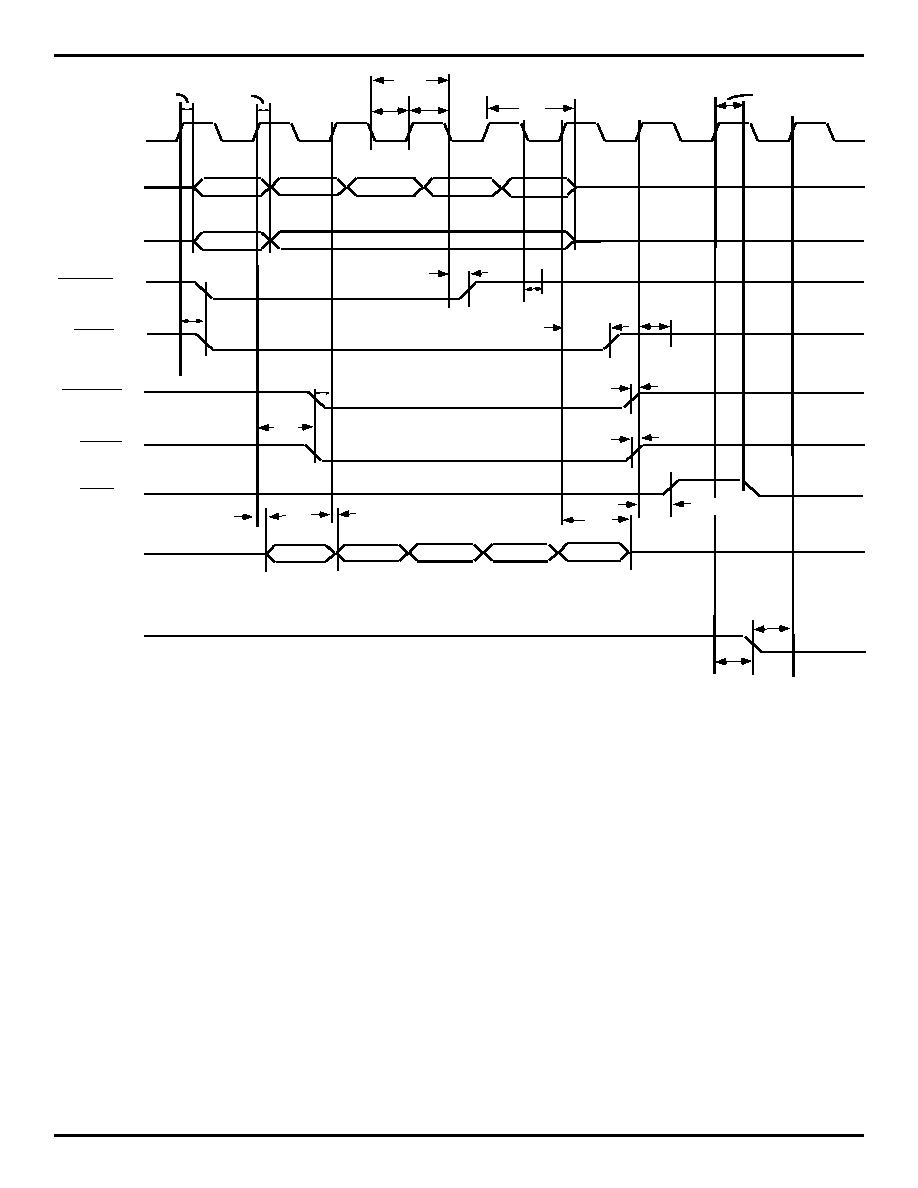
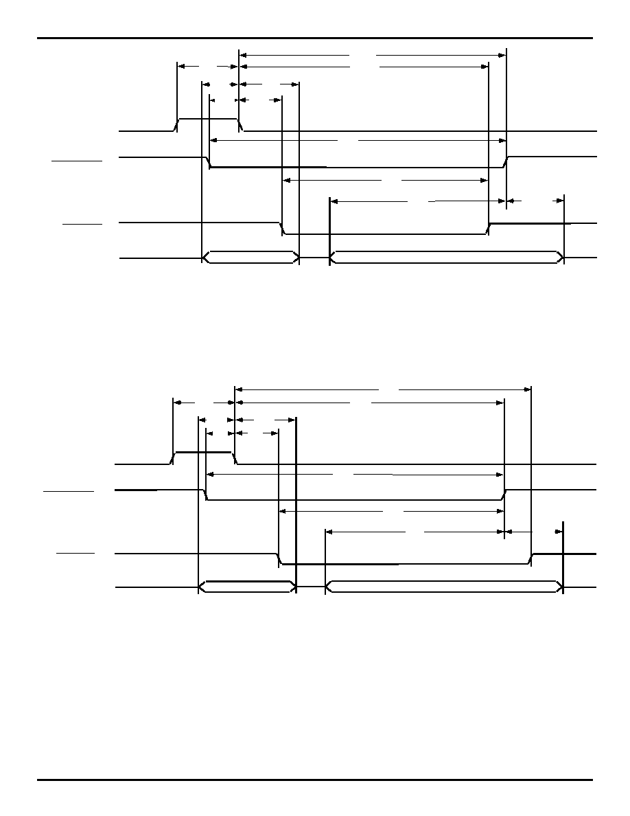
Figure 1. The IDT77222 as a PCI master (illustrates a 4-word write by the IDT77222 to host memory)
PCI_CLK
(I)
FRAME
(O)
C/BE3-0
(O)
AD31-0
(O)
Add
Data0
Data1
Data2
Data3
Cmd
BE3-0
IRDY
(O)
TRDY
(I)
REQ
(O)
DEVSEL
(I)
toff
ton
tval
tval (ptp)
5349 drw 06
ParA
ParD0
ParD1
ParD2
ParD3
tcyc
tlow thigh
ton
tval
tval
tval
toff
tval
tval(ptp)
toff
ton
toff
tsu
tsu
tsu
tsu(ptp)
th
th
PAR
(O)
GNT
(I)
IDT77222 155Mb/s ATM Segmentation & Reassembly (SAR) Controller
PRELIMINARY
with ABR for the PCI Local Bus
COMMERCIAL TEMPERATURE RANGE
18
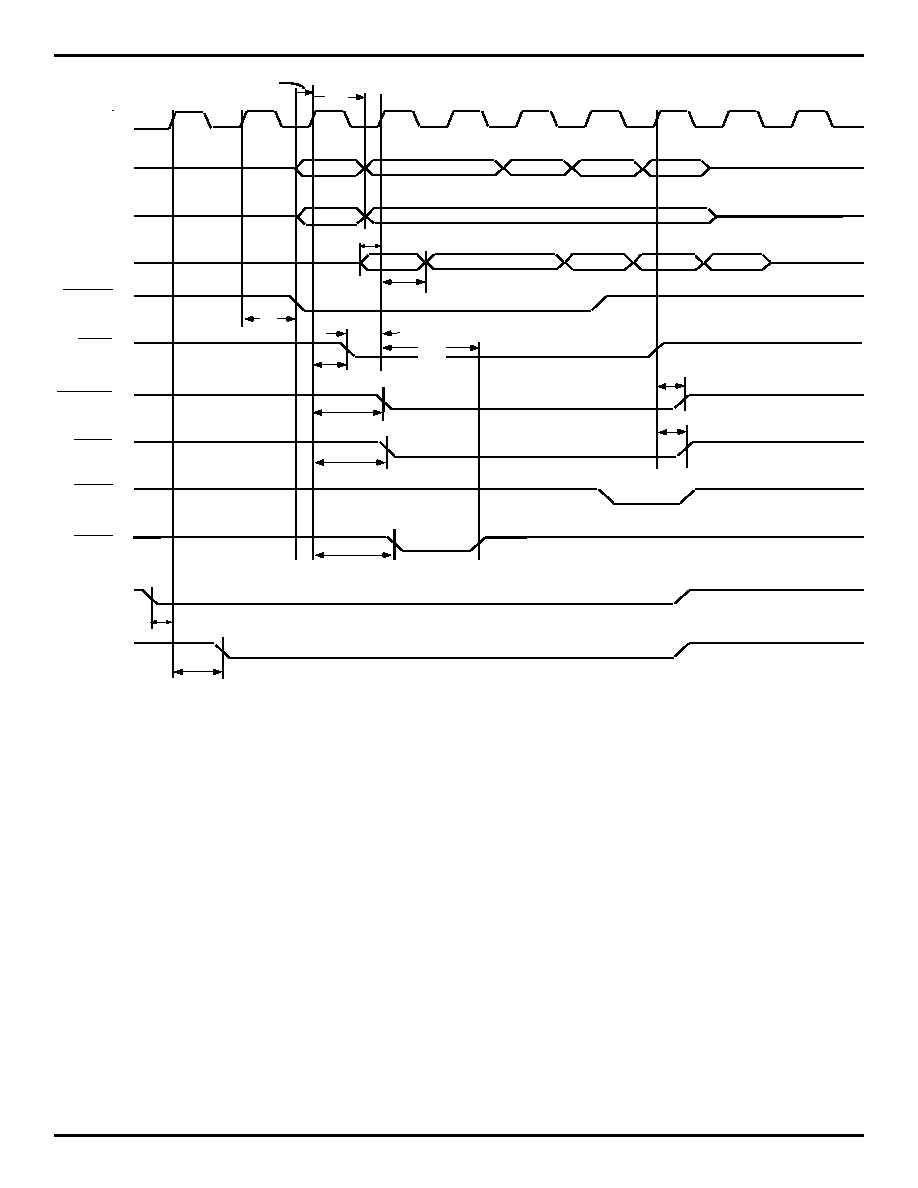
Figure 2. The IDT77222 as a PCI target
(illustrates a 4-word write operation by the host device driver to the IDT77222)
PCI_CLK
(1)
FRAME
(1)
C/BE3-0
(1)
PAR
(1)
AD31-0
(1)
Add
Data0
Data1
Data2
Data3
Cmd
BE3-0
ParD0
ParD1
ParD2
ParD3
ParA
IRDY
(1)
SERR
(O)
TRDY
(O)
PERR
(O)
DEVSEL
(1)
th
tsu
5349 drw 07
tsu
tsu
tsu
th
th
th
toff
toff
toff
tval,
ton
tval,
ton
tval,
ton
tval
REQ#
(1)
REQ
(O)
IDT77222 155Mb/s ATM Segmentation & Reassembly (SAR) Controller
PRELIMINARY
with ABR for the PCI Local Bus
COMMERCIAL TEMPERATURE RANGE
19
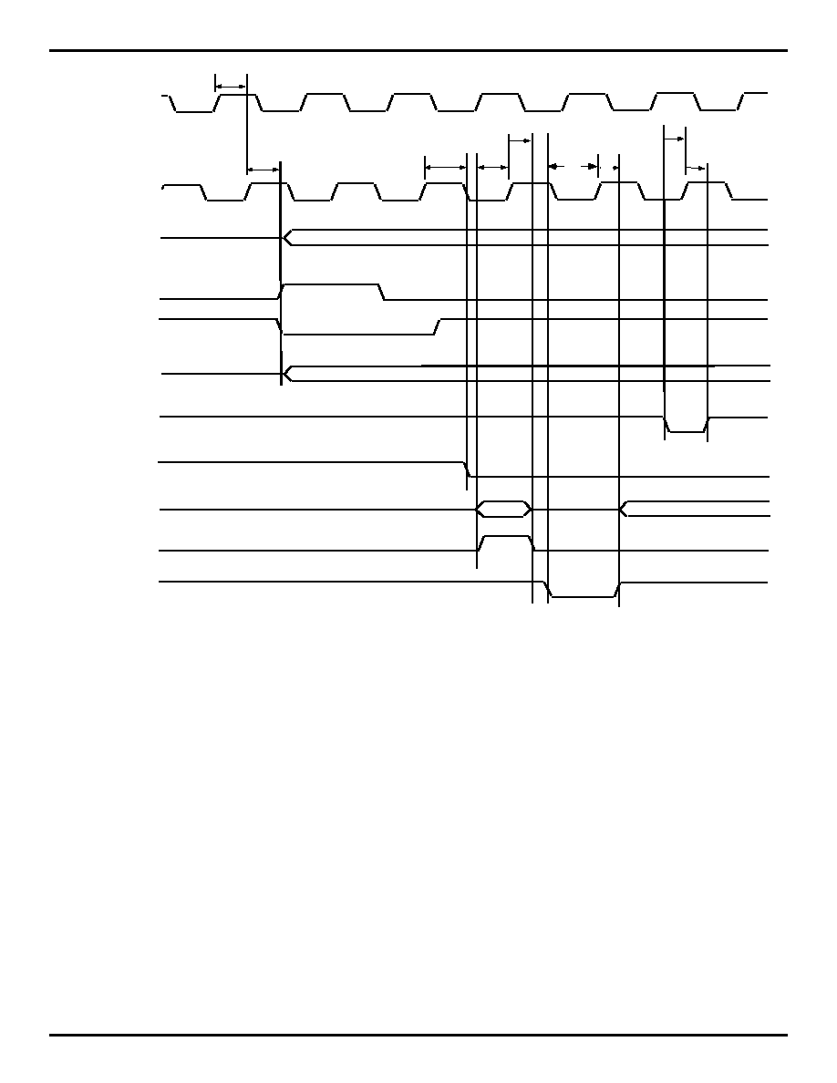
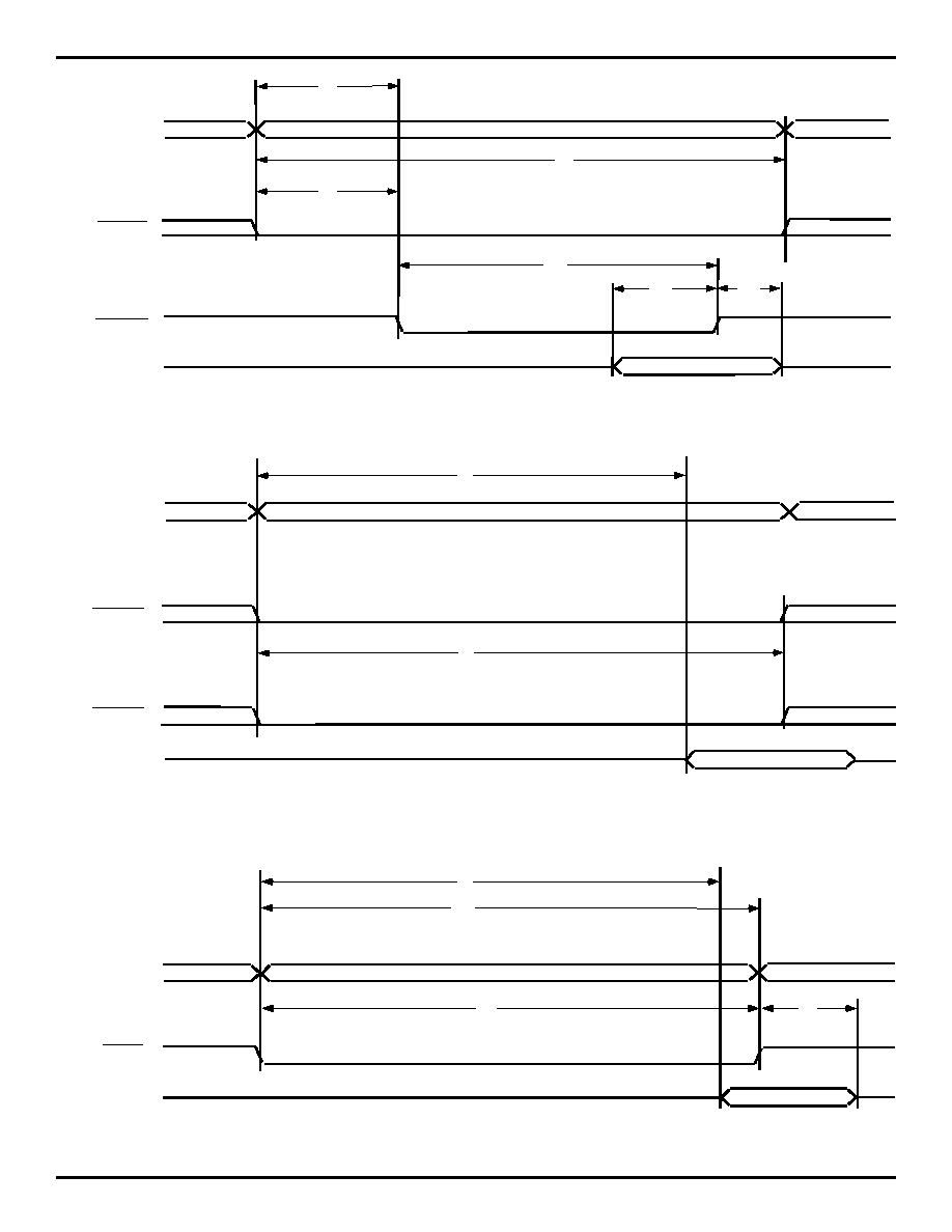
Figure 3. UTOPIA Bus Timing
PHY_Clk
(I)
TxData 7-0
(O)
TxClk,RxClk
(O)
TxSOC
(O)
TxParity
(O)
Txfull
/
TxCLAV
TxEnb
(O)
5349 drw 08
RxEnb
(O)
RxData 7-0
(I)
RxSOC
(I)
RxEmpty
/
(I)
RxCLAV
t1
t2
t5
t7
t9
t6
t8
t3
t4
(I)
IDT77222 155Mb/s ATM Segmentation & Reassembly (SAR) Controller
PRELIMINARY
with ABR for the PCI Local Bus
COMMERCIAL TEMPERATURE RANGE
20
Figure 4. Utility Bus Write Cycle
Figure 5. Utility Bus Read Cycle
UTL_CS0/1
(O)
UTL_WR
(O)
UTL_AD(7-0)
(I/O)
5349 drw 09
UTL_ALE
(O)
tw1
tw3
tw4
tw5
(O)
Valid Data
Address (O)
tw7
tw2
tw10
tw6
tw8
tw9
tw11
UTL_CS0/1
UTL_RD
UTL_AD7-0
5349 drw 10
UTL_ALE
tr1
tr3
tr4
tr5
(I)
Valid Data
Address (O)
tr7
tr2
tr8
tr10
tr9
tr2
tr11
tr6
IDT77222 155Mb/s ATM Segmentation & Reassembly (SAR) Controller
PRELIMINARY
with ABR for the PCI Local Bus
COMMERCIAL TEMPERATURE RANGE
21
SR_CS
SR_WE
SR_I/O(31-0)
5349 drw 11
t1
SR_A(18-0)
t4
t2
t5
t3
t6
SR_I/O(7-0)
5349 drw 13
SR-A (18-0)
t2
Valid Data
t4
E_CE
t1
t3
SR_CS
SR_OE
SR_I/O(31-0)
5349 drw 12
SR_A(18-0)
t1
t2
Figure 6. SRAM Bus Write Cycle Timing
Figure 7. SRAM Bus Read Cycle Timing
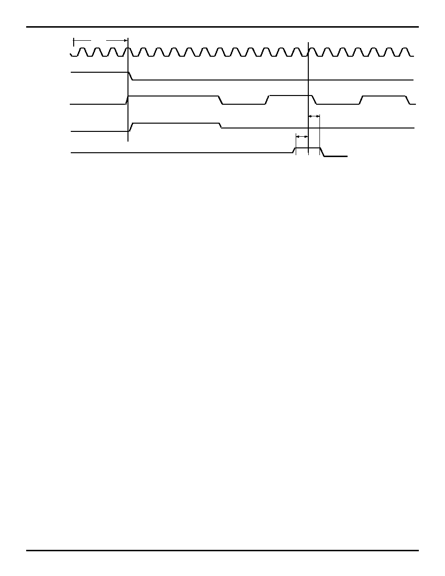
Figure 8. EPROM Timing
IDT77222 155Mb/s ATM Segmentation & Reassembly (SAR) Controller
PRELIMINARY
with ABR for the PCI Local Bus
COMMERCIAL TEMPERATURE RANGE
22
Several software vendors have writen IDT77222 software drivers for various operating systems. Please contact your local
IDT sales representative for a vendor list, or e-mail atmhelp@idt.com.
IDT offers the Sarwin2 demo driver and application suite, which can be used to evaluate the IDT77222 when used with
a IDT NIC reference or evaluation adapter. It may also be used as a reference for sample source code when developing a
proprietary device driver. Please contact your IDT sales representative or e-mail atmhelp@idt.com to obtain a free cdrom.
NIC Reference and Evaluation Adapters
NIC Reference and Evaluation adapters are available in several form factors. Bill of Materials (BOM) and schematics are
available upon request for each of the NIC adapters. A list of current NIC adapter offerings can be found at www.idt.com.
Note: The Micro ABR SAR User Manual provides a detailed description of the 77222 operation and registers.
SAR_CLK
EECLK
EECS
EEDI
EEDO
5349 drw 14
t1
t2
t3
Figure 9. EEPROM Timing
¥
SOFTWARE AND SOFTWARE DRIVERS
IDT77222 155Mb/s ATM Segmentation & Reassembly (SAR) Controller
PRELIMINARY
with ABR for the PCI Local Bus
COMMERCIAL TEMPERATURE RANGE
23
ORDERING INFORMATION
Notes:
Refer to PSC-4053 for detailed package drawing.
Replacing the 77211 with the 77222:
The 77222 PG package is the same package as the 77211 PQF, the 77222 is a direct replacement to the 77211 SAR.
To use the 77222 in a 155 Mbps application a 80 MHz oscillator is required (replace the 50 MHz oscillator used with
the 77211).
PRELIMINARY DATASHEET: DEFINITION
"PRELIMINARY" datasheets contain descriptions for products that are in early release, including features and block
diagrams.
Data Sheet Document History
6/24/98:
Created new document
9/15/99:
Updated software section
6/22/00:
Added PG-208 to package pinout and added PSC-4053 reference. Removed Industrial temp rating.
Changed pin name for pin 198. Updated SRAM, Utility Bus, UTOPIA Bus, EPROM and PCI timing
parameters and diagrams. Updated AC test Conditions section. Added information for NAND Tree.
Changed from Advanced to Preliminary data sheet.
Package
IDT
NNNNN
Device Type
A
Power
NNN
Speed
A
A
Process/
Temp. Range
155
Speed in Mps
77222
155Mbs ATM Segmentation &
Reassembly (SAR) Controller for the
PCI Local Bus
5349 drw 15
PG
208-pin Plastic Quad Flatpack
L
Low Power CMOS
(Blank)
Commercial
Integrated Device Technology, Inc.
2975 Stender Way, Santa Clara, CA 95054-3090
Telephone: (408) 727-6116
FAX 408-330-1748
Integrated Device Technology, Inc. reserves the right to make changes to the specifications in this data sheet in order to improve design or performance and to supply the best possible product.