 | –≠–ª–µ–∫—Ç—Ä–æ–Ω–Ω—ã–π –∫–æ–º–ø–æ–Ω–µ–Ω—Ç: IDT77V252 | –°–∫–∞—á–∞—Ç—å:  PDF PDF  ZIP ZIP |
COMMERCIAL AND INDUSTRIAL TEMPERATURE RANGE
OCTOBER 2000
©1998 Integrated Device Technology, Inc.
DSC-5350/7
1
KEY FEATURES
∑ Full-duplex Segmentation and Reassembly (SAR) at
155 Mbps "wire-speed" (310 Mbps aggregate speed).
∑ Performs ATM layer protocol functions.
∑ Supports AAL5, AAL3/4, AAL0 and Raw Cell formats.
∑ Supports Constant Bit Rate (CBR), Variable Bit Rate
(VBR), and Unassigned Bit Rate (UBR), and Available
Bit Rate (ABR) service classes.
∑ Segments and reassembles CS-PDUs using host
memory.
∑ Four buffer pools for independent or chained reassembly
∑ PCI 2.1 compliant.
∑ Compact PCI R1.0 Hot Swap Friendly compliant.
∑ Operates with ATM networks up to 155.52 Mbps.
∑ Up to 16K open transmit connections.
∑ Up to 16K simultaneous receive connections.
∑ UTOPIA Level 1 Interface to PHY.
∑ UTOPIA Master/Slave mode.
∑ Utility & Management Interface to PHY.
∑ Supports any buffer alignment condition.
∑ Supports Big and Little Endian data transfers.
∑ Free Bufffer Queues mapped into PCI memory space.
∑ Configurable transmit FIFO depth for reduced latency.
∑ Null cell disable option during transmit.
∑ Large Rx FIFO size (configurable to 1024 Kbytes).
∑ Meets Power Management specification.
∑ Automatic AAL5 padding.
∑ UNI 3.1, TM 4.0 compliant.
∑ Buffer management options for efficient MPEG opera-
tion.
∑ Pin compatible with IDT 77211/77252 SAR.
∑ Software compatible with the IDT 77252.
Integrated Device Technology, Inc.
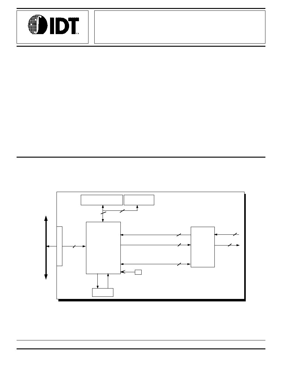
SYSTEM-LEVEL FUNCTIONAL BLOCK DIAGRAM
3.3V 155 Mbps ATM SAR CONTROLLER
WITH ABR SUPPORT FOR PCI-BASED
NETWORKING APPLICATIONS
PRELIMINARY
INFORMATION
IDT77V252
NICStAR is a trademark and the IDT logo is a registered trademark of Integrated Device Technology, Inc.
32
33 M H Z
IDT77V252
155Mbps
P C I A T M
ABR SAR
P H Y
Rx U TO PIA B us
Tx U TO P IA B us
U tility B u s
8
8
8
2
2
155M bps
16K x 32 to 512K x 32
S R A M
EEPROM
32
80.0M HZ O S C.
PCI BUS
PROM
8
5350 drw 01
P
C
I
I
n
t
er
f
a
ce

2
IDT77V252 155Mb/s ATM Segmentation & Reassembly (SAR) Controller
PRELIMINARY
with ABR for the PCI Local Bus
COMMERCIAL AND INDUSTRIAL TEMPERATURE RANGE
.
/
8
P C I
In terface
PCI Bus
T ra nsm it
C o n tro l
T x
U to p ia
In terface
S R A M IN T E R F A C E
R eceive
C o n tro l
R x
U top ia
Interface
T x U to p ia
Bus
S R A M
Bus
R x U to p ia
Bus
U tilit y
E E P R O M O U T
5 3 5 0 d rw 0 2
/
32
E E P R O M IN
/
8
/
8
/
32
Block Diagram of the 77V252 ABR SAR
DESCRIPTION
The IDT77V252 NICStAR
TM
is a member of IDT's family of
products for Asynchronous Transfer Mode (ATM) networks.
The ABR SAR performs both the ATM Adaptation Layer (AAL)
Segmentation and Reassembly (SAR) function and the ATM
layer protocol functions.
A Network Interface Card (NIC) or internetworking product
based on the ABR SAR uses host memory, rather than local
memory, to reassemble Convergence Sublayer Protocol
Data Units (CS-PDUs) from ATM cell payloads received from
the network. When transmitting, as CS-PDUs become ready,
they are queued in host memory and segmented by the ABR
SAR into ATM cell payloads. From this, the ABR SAR then
creates complete 53-byte ATM cells which are sent through
the network. The ABR SAR's on-chip PCI bus master
interface provides efficient, low latency DMA transfers with
the host system, while its UTOPIA interface provides direct
connection to PHY components used in 25.6 Mbps to 155
Mbps ATM networks.
The IDT77V252 is fabricated using state-of-the-art CMOS
technology, providing the highest levels of integration, perfor-
mance and reliability, with the low-power consumption char-
acteristics of CMOS.

IDT77V252 155Mb/s ATM Segmentation & Reassembly (SAR) Controller
PRELIMINARY
with ABR for the PCI Local Bus
COMMERCIAL AND INDUSTRIAL TEMPERATURE RANGE
3
PACKAGE PINOUT
1
Vcc
2
AD(31)
3
AD(30)
4
AD(29)
5
AD(28)
6
AD(27)
7
AD(26)
8
GND
9
GND
10
AD(25)
11
AD(24)
12
C/
BE
(3)
13
IDSEL
14
AD(23)
15
AD(22)
16
GND
17
GND
18
AD(21)
19
Vcc
20
AD(20)
21
AD(19)
22
AD(18)
23
AD(17)
24
AD(16)
25
GND
26
GND
27
C/
BE
(2)
28
Vcc
29
FRAME
30
IRDY
31
TRDY
32
DEVSEL
33
STOP
34
GND
35
GND
36
INTA
37
Vcc
38
PERR
39
SERR
40
PAR
41
C/
BE
(1)
42
AD(15)
43
GND
44
GND
45
AD(14)
46
AD(13)
47
AD(12)
48
AD(11)
49
AD(10)
50
AD(9)
51
AD(8)
52
GND
156
155
154
153
152
151
150
149
148
147
146
145
144
143
142
141
140
139
138
137
136
135
134
133
132
131
130
129
128
127
126
125
124
123
122
121
120
119
118
117
116
115
114
113
112
111
110
109
108
107
106
105
GND
PHY_INT
PHY_RST
UTL_ALE
UTL_RD
UTL_WR
GND
UTL_AD(7)
UTL_AD(6)
UTL_AD(5)
UTL_AD(4)
Vcc
UTL_AD(3)
GND
UTL_AD(2)
UTL_AD(1)
UTL_AD(0)
Vcc
SAR_CLK
GND
SR_I/O(30)
SR_I/O(29)
GND
SR_I/O(28)
SR_I/O(27)
SR_I/O(26)
SR_I/O(25)
SR_I/O(24)
Vcc
SR_I/O(23)
GND
SR_I/O(22)
SR_I/O(21)
EEDO
EEDI
EESCLK
EECS
Vcc
E_CE
SR_I/O(31)
SR_I/O(20)
SR_I/O(19)
SR_I/O(18)
SR_I/O(17)
GND
SR_I/O(16)
SR_I/O(15)
SR_I/O(14)
SR_I/O(13)
SR_I/O(12)
SR_I/O(11)
Vcc
5
3
5
4
5
5
5
6
5
7
5
8
5
9
6
0
6
1
6
2
6
3
6
4
6
5
6
6
6
7
6
8
6
9
7
0
7
1
7
2
7
3
7
4
7
5
7
6
7
7
7
8
7
9
8
0
8
1
8
2
8
3
8
4
8
5
8
6
8
7
8
8
8
9
9
0
9
1
9
2
9
3
9
4
9
5
9
6
9
7
9
8
9
9
1
0
0
1
0
1
1
0
2
1
0
3
1
0
4
V
c
c
G
N
D
C
/
B
E
(
0
)
A
D
(
7
)
V
c
c
A
D
(
6
)
A
D
(
5
)
A
D
(
4
)
G
N
D
S
R
_
A
1
7
A
D
(
3
)
A
D
(
2
)
A
D
(
1
)
A
D
(
0
)
G
N
D
S
R
_
A
1
5
S
R
_
W
E
S
R
_
A
1
3
S
R
_
A
8
S
R
_
A
9
S
R
_
A
1
1
S
R
_
O
E
S
R
_
A
1
0
S
R
_
C
S
S
R
_
A
1
6
G
N
D
S
R
_
A
1
4
V
c
c
S
R
_
A
1
2
S
R
_
A
7
S
R
_
A
6
S
R
_
A
5
S
R
_
A
4
S
R
_
A
3
S
R
_
A
2
S
R
_
A
1
S
R
_
A
0
S
R
_
A
1
8
G
N
D
S
R
_
I
/
O
(
0
)
S
R
_
I
/
O
(
1
)
S
R
_
I
/
O
(
2
)
S
R
_
I
/
O
(
3
)
S
R
_
I
/
O
(
4
)
S
R
_
I
/
O
(
5
)
S
R
_
I
/
O
(
6
)
G
N
D
S
R
_
I
/
O
(
7
)
S
R
_
I
/
O
(
8
)
S
R
_
I
/
O
(
9
)
S
R
_
I
/
O
(
1
0
)
G
N
D
208 2
0
7
2
0
6
2
0
5
2
0
4
2
0
3
2
0
2
2
0
1
2
0
0
1
9
9
1
9
8
1
9
7
1
9
6
1
9
5
1
9
4
1
9
3
1
9
2
1
9
1
1
6
1
1
9
0
1
8
9
1
8
8
1
8
7
1
8
6
1
8
5
1
8
4
1
8
3
1
8
2
1
8
1
1
8
0
1
7
9
1
7
8
1
7
7
1
7
6
1
7
5
1
7
4
1
7
3
1
7
2
1
7
1
1
7
0
1
6
9
1
6
8
1
6
7
1
6
6
1
6
5
1
6
4
1
6
3
1
6
2
1
6
0
1
5
9
1
5
8
1
5
7
G
N
D
V
c
c
R
E
Q
G
N
T
C
L
K
R
S
T
G
N
D
T
E
S
T
[
0
]
H
S
_H
A
N
D
LE
V
c
c
V
c
c
H
S
_
E
N
U
M
U
T
O
P
I
A
_
M
O
D
E
T
X
P
A
R
I
T
Y
P
H
Y
_
C
L
K
R
X
C
L
K
G
N
D
R
X
_
C
T
R
L
_
I
N
R
X
_
C
T
R
L
_
O
U
T
R
X
D
A
T
A
(
7
)
R
X
D
A
T
A
(
6
)
R
X
D
A
T
A
(
5
)
R
X
D
A
T
A
(
4
)
G
N
D
R
X
D
A
T
A
(
3
)
R
X
D
A
T
A
(
2
)
R
X
D
A
T
A
(
1
)
R
X
D
A
T
A
(
0
)
G
N
D
T
X
C
L
K
T
X
_
C
T
R
L
_
I
N
T
X
_
C
T
R
L
_
O
U
T
T
X
S
O
C
G
N
D
T
X
D
A
T
A
(
7
)
T
X
D
A
T
A
(
6
)
V
C
C
T
X
D
A
T
A
(
5
)
T
X
D
A
T
A
(
4
)
G
N
D
T
X
D
A
T
A
(
3
)
T
X
D
A
T
A
(
2
)
T
X
D
A
T
A
(
1
)
T
X
D
A
T
A
(
0
)
U
T
L
_C
S
(
1
)
U
T
L
_
C
S
(
0
)
V
c
c
Index
5350 drw 03
R
X
S
O
C
T
E
S
T
[1
]
C
LK
_O
U
T
N
C
H
S
_LE
D
IDT77V252 SAR Controller
With ABR Support
208 Pin PQFP
Pinout
PU-208
Refer to PSC-4053 for
detailed package drawing
4
IDT77V252 155Mb/s ATM Segmentation & Reassembly (SAR) Controller
PRELIMINARY
with ABR for the PCI Local Bus
COMMERCIAL AND INDUSTRIAL TEMPERATURE RANGE
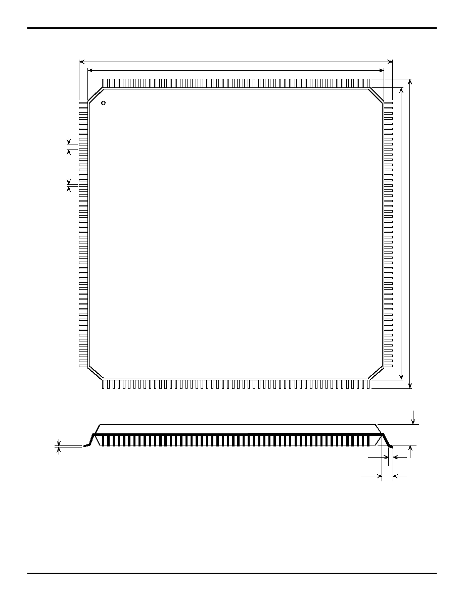
PACKAGE DRAWING
1
52
156
105
53
104
208
157
Index
1.228 ±0.016 (31.2 ±0.4)
1.10 ±0.004 (28.0 ±0.1)
1
.
228
±0
.0
16
(3
1.
2
±
0
.4
)
1.
1
0
±
0
.0
04
(28.
0
±0
.1
)
0.02 ±0.004
(0.5 ±0.1)
0.008 ±0.004
(0.2 ±0.1)
0.024 ±0.008
(0.6 ±0.2)
0.063 (1.6)
0.013 ±0.002
(0.33 ±0.06)
0.133 ±0.004
(3.37 ±0.1)
5350 drw 04

IDT77V252 155Mb/s ATM Segmentation & Reassembly (SAR) Controller
PRELIMINARY
with ABR for the PCI Local Bus
COMMERCIAL AND INDUSTRIAL TEMPERATURE RANGE
5
PIN DEFINITIONS
Pin #
Name
I/O
Bus Name
Description
1
V
C C
I
pow er
2
A D (31)
I/O
P C I
address/data line
3
A D (30)
I/O
P C I
address/data line
4
A D (29)
I/O
P C I
address/data line
5
A D (28)
I/O
P C I
address/data line
6
A D (27)
I/O
P C I
address/data line
7
A D (26)
I/O
P C I
address/data line
8
G N D
I
pow er
9
G N D
I
pow er
10
A D (25)
I/O
P C I
address/data line
11
A D (24)
I/O
P C I
address/data line
12
C /
BE(3)
I/O
P C I
bus com m and
13
ID S E L
I
P C I
bus ID select
14
A D (23)
I/O
P C I
address/data line
15
A D (22)
I/O
P C I
address/data line
16
G N D
I
pow er
17
G N D
I
pow er
18
A D (21)
I/O
P C I
address/data line
19
V
C C
I
pow er
20
A D (20)
I/O
P C I
address/data line
21
A D (19)
I/O
P C I
address/data line
22
A D (18)
I/O
P C I
address/data line
23
A D (17)
I/O
P C I
address/data line
24
A D (16)
I/O
P C I
address/data line
25
G N D
I
pow er
26
G N D
I
pow er
27
C /
BE(2)
I/O
P C I
bus com m and
28
V
C C
I
pow er
29
Frame
I/O
P C I
cy cle fram e
30
IRDY
I/O
P C I
initiator ready
31
TRDY
I/O
P C I
target ready
32
DEVSEL
I/O
P C I
target ind icating address decode
33
STOP
I/O
P C I
target req uesting m aster to stop
34
G N D
I
pow er
35
G N D
I
pow er
36
INTA
O
P C I
"interrupt" "A " "request"
37
V
C C
I
pow er
38
PERR
I/O
P C I
data parity error
39
SERR
O
P C I
sy stem error
40
PAR
I/O
P C I
parity (for A D [0:31] and C /B E[0:3])
41
C /
BE(1)
I/O
P C I
bus com m and
42
A D (15)
I/O
P C I
address/data line
43
G N D
I
pow er
44
G N D
I
pow er
45
A D (14)
I/O
P C I
address/data line
46
A D (13)
I/O
P C I
address/data line
47
A D (12)
I/O
P C I
address/data line
48
A D (11)
I/O
P C I
address/data line
5350 tbl 01

6
IDT77V252 155Mb/s ATM Segmentation & Reassembly (SAR) Controller
PRELIMINARY
with ABR for the PCI Local Bus
COMMERCIAL AND INDUSTRIAL TEMPERATURE RANGE
PIN DEFINITIONS (CON'T.)
Pin #
Name
I/O
Bus Name
Description
4 9
A D ( 1 0 )
I /O
P C I
a d d r e s s / d a t a line
5 0
A D ( 9 )
I /O
P C I
a d d r e s s / d a t a line
5 1
A D ( 8 )
I /O
P C I
a d d r e s s / d a t a line
5 2
G ND
I
p o w e r
5 3
V
CC
I
p o w e r
5 4
G ND
I
p o w e r
5 5
C /
BE
( 0 )
I /O
P C I
b us c o m m a nd
5 6
A D ( 7 )
I /O
P C I
a d d r e s s / d a t a line
5 7
V
CC
I
p o w e r
5 8
A D ( 6 )
I /O
P C I
a d d r e s s / d a t a line
5 9
A D ( 5 )
I /O
P C I
a d d r e s s / d a t a line
6 0
A D ( 4 )
I /O
P C I
a d d r e s s / d a t a line
6 1
G ND
I
p o w e r
6 2
S R _ A 1 7
O
S R A M
A d d re s s line
6 3
A D ( 3 )
I /O
P C I
a d d r e s s / d a t a line
6 4
A D ( 2 )
I /O
P C I
a d d r e s s / d a t a line
6 5
A D ( 1 )
I /O
P C I
a d d r e s s / d a t a line
6 6
A D ( 0 )
I /O
P C I
a d d r e s s / d a t a line
6 7
G ND
I
p o w e r
6 8
S R _ A 1 5
O
S R A M
A d d re s s line
6 9
SR_WE
O
S R A M
W r ite e na b le
7 0
S R _ A 1 3
O
S R A M
A d d re s s line
7 1
S R _ A 8
O
S R A M
A d d re s s line
7 2
S R _ A 9
O
S R A M
A d d re s s line
7 3
S R _ A 11
O
S R A M
A d d re s s line
7 4
SR_OE
O
S R A M
O u tp ut E na b le c o ntr o l
7 5
S R _ A 1 0
O
S R A M
A d d re s s line
7 6
SR_CS
O
S R A M
C hip S e le c t
7 7
S R _ A 1 6
O
S R A M
A d d re s s line
7 8
G ND
I
p o w e r
7 9
S R _ A 1 4
O
S R A M
A d d re s s line
8 0
V
CC
I
p o w e r
8 1
S R _ A 1 2
O
S R A M
A d d re s s line
8 2
S R _ A 7
O
S R A M
A d d re s s line
8 3
S R _ A 6
O
S R A M
A d d re s s line
8 4
S R _ A 5
O
S R A M
A d d re s s line
8 5
S R _ A 4
O
S R A M
A d d re s s line
8 6
S R _ A 3
O
S R A M
A d d re s s line
8 7
S R _ A 2
O
S R A M
A d d re s s line
8 8
S R _ A 1
O
S R A M
A d d re s s line
8 9
S R _ A 0
O
S R A M
A d d re s s line
9 0
S R _ A 1 8
O
S R A M
A d d re s s line
9 1
G ND
I
p o w e r
9 2
S R _ I/O (0 )
I /O
S R A M
D a ta inp ut /o ut p ut line
9 3
S R _ I/O (1 )
I /O
S R A M
D a ta inp ut /o ut p ut line
9 4
S R _ I/O (2 )
I /O
S R A M
D a ta inp ut /o ut p ut line
9 5
S R _ I/O (3 )
I /O
S R A M
D a ta inp ut /o ut p ut line
9 6
S R _ I/O (4 )
I /O
S R A M
D a ta inp ut /o ut p ut line
5350 t bl 0 2

IDT77V252 155Mb/s ATM Segmentation & Reassembly (SAR) Controller
PRELIMINARY
with ABR for the PCI Local Bus
COMMERCIAL AND INDUSTRIAL TEMPERATURE RANGE
7
PIN DEFINITIONS (CON'T.)
Pin #
Name
I/O
Bus Name
Description
9 7
S R _ I/O (5 )
I /O
S R A M
D a ta inp ut /o ut p ut line
9 8
G ND
I
p o w e r
9 9
S R _ I/O (6 )
I /O
S R A M
D a ta inp ut /o ut p ut line
1 0 0
S R _ I/O (7 )
I /O
S R A M
D a ta inp ut /o ut p ut line
1 0 1
S R _ I/O (8 )
I /O
S R A M
D a ta inp ut /o ut p ut line
1 0 2
S R _ I/O (9 )
I /O
S R A M
D a ta inp ut /o ut p ut line
1 0 3
S R _ I /O ( 1 0 )
I /O
S R A M
D a ta inp ut /o ut p ut line
1 0 4
G ND
I
p o w e r
1 0 5
V
CC
I
p o w e r
1 0 6
S R _ I/ O (11 )
I /O
S R A M
D a ta inp ut /o ut p ut line
1 0 7
S R _ I /O ( 1 2 )
I /O
S R A M
D a ta inp ut /o ut p ut line
1 0 8
S R _ I /O ( 1 3 )
I /O
S R A M
D a ta inp ut /o ut p ut line
1 0 9
S R _ I /O ( 1 4 )
I /O
S R A M
D a ta inp ut /o ut p ut line
11 0
S R _ I /O ( 1 5 )
I /O
S R A M
D a ta inp ut /o ut p ut line
111
S R _ I /O ( 1 6 )
I /O
S R A M
D a ta inp ut /o ut p ut line
11 2
G ND
I
p o w e r
11 3
S R _ I /O ( 1 7 )
I /O
S R A M
D a ta inp ut /o ut p ut line
11 4
S R _ I /O ( 1 8 )
I /O
S R A M
D a ta inp ut /o ut p ut line
11 5
S R _ I /O ( 1 9 )
I /O
S R A M
D a ta inp ut /o ut p ut line
11 6
S R _ I /O ( 2 0 )
I /O
S R A M
D a ta inp ut /o ut p ut line
11 7
S R _ I /O ( 2 1 )
I /O
S R A M
D a ta inp ut /o ut p ut line
11 8
S R _ I /O ( 2 2 )
I /O
S R A M
D a ta inp ut /o ut p ut line
11 9
G ND
I
p o w e r
1 2 0
S R _ I /O ( 2 3 )
I /O
S R A M
D a ta inp ut /o ut p ut line
1 2 1
V
CC
I
p o w e r
1 2 2
S R _ I /O ( 2 4 )
I /O
S R A M
D a ta inp ut /o ut p ut line
1 2 3
S R _ I /O ( 2 5 )
I /O
S R A M
D a ta inp ut /o ut p ut line
1 2 4
S R _ I /O ( 2 6 )
I /O
S R A M
D a ta inp ut /o ut p ut line
1 2 5
S R _ I /O ( 2 7 )
I /O
S R A M
D a ta inp ut /o ut p ut line
1 2 6
S R _ I /O ( 2 8 )
I /O
S R A M
D a ta inp ut /o ut p ut line
1 2 7
G ND
I
p o w e r
1 2 8
S R _ I /O ( 2 9 )
I /O
S R A M
D a ta inp ut /o ut p ut line
1 2 9
S R _ I /O ( 3 0 )
I /O
S R A M
D a ta inp ut /o ut p ut line
1 3 0
S R _ 1 / O ( 3 1 )
I /O
S R A M
D a ta inp ut /o ut p ut line
1 3 1
E_CE
O
E P R O M
E P R O M c hip s e le c t
1 3 2
V
CC
I
p o w e r
1 3 3
E E C S
O
E E P R O M
c hip s e le c t
1 3 4
E E S C L K
O
E E P R O M
c lo c k
1 3 5
E E D I
I
E E P R O M
D a t a inp ut
1 3 6
E E D O
O
E E P R O M
D a t a o ut p ut
1 3 7
G ND
I
p o w e r
1 3 8
S A R _ C L K
I
S A R c lo c k inp ut
1 3 9
V
CC
I
p o w e r
1 4 0
UT L _ A D ( 0 )
I /O
Ut ility
a d d r e s s / d a t a b us
1 4 1
UT L _ A D ( 1 )
I /O
Ut ility
a d d r e s s / d a t a b us
1 4 2
UT L _ A D ( 2 )
I /O
Ut ility
a d d r e s s / d a t a b us
1 4 3
G ND
I
p o w e r
1 4 4
UT L _ A D ( 3 )
I /O
Ut ility
a d d r e s s / d a t a b us
53 50 tb l 0 3

8
IDT77V252 155Mb/s ATM Segmentation & Reassembly (SAR) Controller
PRELIMINARY
with ABR for the PCI Local Bus
COMMERCIAL AND INDUSTRIAL TEMPERATURE RANGE
PIN DEFINITIONS (CON'T.)
Pin #
Name
I/O
Bus Name
Description
1 4 5
V
CC
I
p o w e r
1 4 6
UT L _ A D ( 4 )
I /O
Ut ility
a d d r e s s / d a t a b us
1 4 7
UT L _ A D ( 5 )
I /O
Ut ility
a d d r e s s / d a t a b us
1 4 8
UT L _ A D ( 6 )
I /O
Ut ility
a d d r e s s / d a t a b us
1 4 9
UT L _ A D ( 7 )
I /O
Ut ility
a d d r e s s / d a t a b us
1 5 0
G ND
I
p o w e r
1 5 1
UTL_WR
O
Ut ility
w rite c o nt ro l
1 5 2
UTL_RD
O
Ut ility
r e a d c o nt r o l
1 5 3
UT L _ A L E
O
Ut ility
a d d re s s la t c h e na b le
1 5 4
PHY_RST
O
P HY
r e s t c o nt ro l
1 5 5
PHY_INT
I
P HY
inte r r up t inp ut fr o m P HY
1 5 6
G ND
I
p o w e r
1 5 7
V
CC
I
p o w e r
1 5 8
UTL_CS(0)
O
Ut ility
c hip s e le c t ( 0 )
1 5 9
UTL_CS(1)
O
Ut ility
c hip s e le c t ( 1 )
1 6 0
T xD a t a ( 0 )
O
UT O P IA
tr a ns m it d a t a b it 0
1 6 1
T xD a t a ( 1 )
O
UT O P IA
tr a ns m it d a t a b it 1
1 6 2
T xD a t a ( 2 )
O
UT O P IA
tr a ns m it d a t a b it 2
1 6 3
T xD a t a ( 3 )
O
UT O P IA
tr a ns m it d a t a b it 3
1 6 4
G ND
I
p o w e r
1 6 5
T xD a t a ( 4 )
O
UT O P IA
tr a ns m it d a t a b it 4
1 6 6
T xD a t a ( 5 )
O
UT O P IA
tr a ns m it d a t a b it 5
1 6 7
V
CC
I
p o w e r
1 6 8
T xD a t a ( 6 )
O
UT O P IA
tr a ns m it d a t a b it 6
1 6 9
T xD a t a ( 7 )
O
UT O P IA
tr a ns m it d a t a b it 7
1 7 0
G ND
I
p o w e r
1 7 1
T xS O C
O
UT O P IA
t r a ns m it s ta r t o f c e ll
1 7 2
T x_ C t r l_ O ut
O
UT O P IA
t ra ns m it c o ntr o l o utp ut ( s e e D ia g r a m 5 )
1 7 3
T x_ C tr l_ In
I
UT O P IA
t ra ns m it c o nt ro l inp ut (s e e D ia g r a m 5 )
1 7 4
T xC L K
I /O
UT O P IA
t ra ns m it d a t a s y nc c lo c k
1 7 5
G ND
I
p o w e r
1 7 6
R xD a t a ( 0 )
I
UT O P I A
r e c e ive d a ta b it 0
1 7 7
R xD a t a ( 1 )
I
UT O P IA
r e c e ive d a ta b it 1
1 7 8
R xD a t a ( 2 )
I
UT O P IA
r e c e ive d a ta b it 2
1 7 9
R xD a t a ( 3 )
I
UT O P IA
r e c e ive d a ta b it 3
1 8 0
G ND
I
p o w e r
1 8 1
R xD a t a ( 4 )
I
UT O P IA
r e c e ive d a ta b it 4
1 8 2
R xD a t a ( 5 )
I
UT O P IA
r e c e ive d a ta b it 5
1 8 3
R xD a t a ( 6 )
I
UT O P IA
r e c e ive d a ta b it 6
1 8 4
R xD a t a ( 7 )
I
UT O P IA
r e c e ive d a ta b it 7
1 8 5
R xS O C
I
UT O P IA
r e c e ive s ta r t o f c e ll
1 8 6
R x_ C t rl_ O ut
O
UT O P IA
r e c e ive c o nt ro l o utp ut ( s e e D ia g r a m 5 )
1 8 7
R x_ C t rl_ I n
I
UT O P IA
r e c e ive c o nt ro l inp ut ( s e e D ia g r a m 5 )
1 8 8
G ND
I
p o w e r
1 8 9
R xC lk
I /O
UT O P IA
r e c e ive d a t a s y nc c lo c k
1 9 0
P HY _ C lk
I
UT O P IA
t ra ns m it s y nc c lo c k inp ut
1 9 1
T xP a r it y
O
UT O P IA
t ra n s m it d a ta p a r ity b it
1 9 2
UT O P IA _ M o d e
I
UT O P IA
UT O P IA M a s te r /S la ve m o d e s e le c t ( "0 " = M a s t e r ; "1 " = S la ve )
53 50 tb l 0 4

IDT77V252 155Mb/s ATM Segmentation & Reassembly (SAR) Controller
PRELIMINARY
with ABR for the PCI Local Bus
COMMERCIAL AND INDUSTRIAL TEMPERATURE RANGE
9
PIN DEFINITIONS (CON'T.)
Pin #
Name
I/O
B us Name
Description
1 93
HS_LED
O
P C I
ho t sw a p frie ndly s ta tus LE D
1 94
HS_Enum
O
P C I
hot s w a p frie ndly c o nfig ura tion sig nal
1 95
NC
---
---
no co nnec tio n
1 96
V
CC
I
p ow e r
1 97
V
CC
I
p ow e r
1 98
C LK o ut
O
S A R _ C lk d ivid ed b y 3
1 99
HS_Handle
I
P C I
hot s w a p frie nd ly ha nd le sw itch
2 00
Tes t[1]
I
p ow e r
te s t m o d e c ontro l (se e Tab le 1 )
2 01
Tes t[0]
I
p ow e r
te s t m o d e c ontro l (se e Tab le 1 )
2 02
G ND
I
p ow e r
2 03
RST
I
P C I
s yste m b us re se t
2 04
C LK
I
P C I
b us clo c k
2 05
GNT
I
P C I
b us g ra n t sig na l from a rb ite r
2 06
REQ
O
P C I
b us req ues t
2 07
V
CC
I
p ow e r
2 08
G ND
I
p ow e r
53 50 tb l 0 5

10
IDT77V252 155Mb/s ATM Segmentation & Reassembly (SAR) Controller
PRELIMINARY
with ABR for the PCI Local Bus
COMMERCIAL AND INDUSTRIAL TEMPERATURE RANGE
ABSOLUTE MAXIMUM RATINGS
RECOMMENDED OPERATING CONDITIONS
Symbol
Parameter
M in.
M ax.
Unit
V
CC
S up p ly Vo lta g e
V
S S
- 0 .3
3 .6
V
V
IN
Inp ut Vo lta g e
V
S S
- 0 .3
V
CC
+ 0 .3
V
V
O UT
O utp ut Vo lta g e
V
S S
- 0 .3
V
CC
+ 0 .3
V
V
S S
G ro und Vo lta g e
0
0
V
T
s t g
S t o ra g e Te m p e ra t ure
-5 5
1 2 5
∞C
5 3 5 0 tb l 0 6
CLOCKING
Symbol
Parameter
Min.
Max.
Unit
V
CC
Supply Voltage
3.0
3.6
V
V
I
Input Voltage
0
V
CC
V
T
A1
Commerical operating temperature
0
+70
∞C
T
A2
Industrial operating temperature
-40
+85
∞C
titr
Input TTL rise time
____
2
ns
titf
Input TTL rall time
____
2
ns
5350 tbl 07
CAPACITANCE
Symbol
Parameter
Rate
Min.
Max.
Unit
SAR_CLK
SAR clock input freq.
155Mb/s
77
80
MHz
25Mb/s
25
80
MHz
PHY_CLK
PHY clock input freq.
155Mb/s
19.44
40
MHz
25Mb/s
3
40
MHz
PCI_CLK
PCI clock input freq.
33MHz
0
33.3
MHz
5350 tbl 08
Symbol
Parameter
Condition
Min.
Max.
Typical
Unit
C
IN
Input Capacitance
except PCI Bus
____
____
4
pF
C
OUT
Output Capacitance
all outputs
____
8
6
pF
C
bid
Bi-Directional Capacitance
all bi-directional pins
____
____
10
pF
C
inpci
PCI Bus Input Capacitance
PCI Bus inputs
____
10
____
pF
C
clkpci
PCI Bus Clock Input Capacitance
____
5
12
____
pF
C
idsel
PCI Bus ID Select Input Capacitance
____
____
8
____
pF
5350 tbl 09

IDT77V252 155Mb/s ATM Segmentation & Reassembly (SAR) Controller
PRELIMINARY
with ABR for the PCI Local Bus
COMMERCIAL AND INDUSTRIAL TEMPERATURE RANGE
11
DC OPERATING CONDITIONS
Symbol
Parameter
Condition
M in.
M ax.
Typical
Unit
V il
Low -le ve l T T L input volta ge
____
-0.7V
(0.3)V
CC
____
V
V ih
High-le vel T T L input voltage
____
(0.5)V
CC
V
CC
+ 0.2V
____
V
Vol
Low -lev el T T L o utput volta ge
____
____
0.4
____
V
Voh
High-level T T L output voltage
____
V
CC
- 0.4V
____
____
V
Iol
Low -lev el T T L o utput c urrent:
S R _ A (1 8-0)
V
S S
+ 0.4V
12
____
____
m A
Ioh
High-leve l T T L output c urrent:
S R _ A (1 8-0)
V
CC
- 0.4V
-4
____
____
m A
Iol
Low -lev el T T L o utput c urrent:
R x_C trl_ O ut, R xC lk , T xS O C ,
T xD ata (7-0 ), T x_C trl_O ut, T xParity,
T xC lk,
WE
,
OE
,
CS
,
S R _ D 3 1-0
V
S S
+ 0.4V
6
____
____
m A
Ioh
High-leve l T T L output c urrent:
R x_C t rl_O ut, R xC lk, T xS oc,
T xD a ta7-0, T x_C trl_ O ut, T xPa rity,
T xC lk,
SR_WE
,
SR
,
OE
,
SR_CS
,
S R _ I/O (31-0)
V
CC
- 0.4V
-2
____
____
m A
Iol
Low -lev el T T L o utput c urrent:
UT L_A D (7-0),
UTL_RD
,
UTL_WR
, UT L_A LE ,
UTL_CS0/1
, E E SC L K, E E C S,
E E D O ,
PHY_RST
V
S S
+ 0.4V
3
____
____
m A
Ioh
High-leve l T T L output c urrent:
UT L_A D (7-0_,
UTL_RD
,
UTL_WR
, UT L_A LE ,
UTL_CS0/1
, E E SC L K, E E C S,
E E D O ,
PHY_RST
V
CC
- 0.4V
-1
____
____
m A
Iil
Input leak age c urrent
V
S S
< V
IN
< V dd
-1
1
____
uA
Ityp
D y nam ic S up ply C urre nt
____
____
300
195
m A
5350 tbl 10

12
IDT77V252 155Mb/s ATM Segmentation & Reassembly (SAR) Controller
PRELIMINARY
with ABR for the PCI Local Bus
COMMERCIAL AND INDUSTRIAL TEMPERATURE RANGE
AC OPERATING CONDITIONS
AC TEST CONDITIONS
Input Pulse Levels
0 to 3.0V
Input Rise/Fall Times
2ns
Input Timing Ref. Level
1.5V
Output Ref. Level
1.5V
AC Test Load
See Figure Below
5350 tbl 11
1.5V
50
I/O
Z
0
= 50
1
2
3
4
20 30 50
100
200
tCD
(Typical, ns)
Capacitance (pF)
80
5
6
5350 drw 05
7 7 V 2 5 2
A T M d e vic e
T x D a ta
T xP a rity
T x S o c
T x _ C trl_ O u t
T x_ C trl_ In
R x D a ta
R xS o c
R x _ C trl_ O u t
R x _ C trl_ In
U T O P IA _ C lk
T xD a ta
R x P a rity
T xS o c
TxEnb
T xC la v
R x D a ta
R x S o c
RxEnb
R x C la v
U T O P IA _ C lk
5 3 5 0 d rw 0 6
T xD a ta
T x P a rity
T xS o c
T x _ C trl_ O u t
T x_ C trl_ In
7 7 V 2 5 2
P H Y d e v ic e
R xD a ta
R x S o c
R x_ C trl_ O u t
R x_ C trl_ In
U T O P IA _ C lk
T x D a ta
T x P a rity
T x S o c
TxEnb
T x C la v
R x D a ta
R x S o c
RxEnb
R x C la v
U T O P IA _ C lk
U T O P IA M as te r
U T O P IA S la ve
Diagram 5. UTOPIA Modes
IDT77V252 155Mb/s ATM Segmentation & Reassembly (SAR) Controller
PRELIMINARY
with ABR for the PCI Local Bus
COMMERCIAL AND INDUSTRIAL TEMPERATURE RANGE
13
NAND CHAIN
The NAND Chain provides a simple test to verify that all bond wires are installed correctly and that all pads are correctly
soldered on a PCB.
All signal pads are linked in a NAND chain, which is enabled by asserting a high, or "1", on Test[0] (pin 201), and a low,
or "0" on Test[1] (pin 200). Asserting a "1" on the other inputs forces EEDO (pin 136) to "1". By successively setting the
inputs to "0", starting at
HS_Handle
(pin 199) and moving to
RST
(pin 203), EEDO will toggle with each change.
1. Apply a "1" to Test[0] and a "0" to Test[1].
2. Set all the I/O's in the chain to "0" and EEDO should be a "1".The connection order of the pins in the chain are shown
in the NAND Tree Pin Order table located on the following page.
3. Set
HS_Handle
to a "0" and the EEDO should be a "0".
4. Leaving
HS_Handle
at a "1" set
HS_Enum
to "1" and EEDO should be a "1".
5. Repeat for all remaining I/O's in the NAND chain.
Test[0]
Test[1]
M ode
0
0
Norm al operation.
0
1
NA ND test. EE DO (pin 136) is the output of the NA ND chain w hen
using the NA ND test m ode.
1
0
S can test. EED I (pin 135) is scan data input , E EDO (pin 136) is
scan data output, and EES C LK (pin 134) is scan clock.
1
1
O utput test. All outputs eq ual EED I (pin 135).
53 50 tbl 12
Table 1. Test Modes

14
IDT77V252 155Mb/s ATM Segmentation & Reassembly (SAR) Controller
PRELIMINARY
with ABR for the PCI Local Bus
COMMERCIAL AND INDUSTRIAL TEMPERATURE RANGE
NAND
Tree O rder
Pin
#
NAND Tree
O rder
Pin
#
NAND Tree
O rder
Pin
#
NAND Tree
O rder
Pin
#
NAND Tree
O rder
Pin
#
1
1 9 9
3 2
1 5 8
6 3
11 5
9 4
7 6
1 2 5
3 6
2
1 9 4
3 3
1 5 5
6 4
11 4
9 5
7 5
1 2 6
3 3
3
1 9 3
3 4
1 5 4
6 5
11 3
9 6
7 4
1 2 7
3 2
4
1 9 2
3 5
1 5 3
6 6
111
9 7
7 3
1 2 8
3 1
5
1 9 1
3 6
1 5 2
6 7
1 0 9
9 8
7 2
1 2 9
3 0
6
1 9 0
3 7
1 5 1
6 8
1 0 8
9 9
7 1
1 3 0
2 9
7
1 8 9
3 8
1 4 9
6 9
1 0 7
1 0 0
7 0
1 3 1
2 7
8
1 8 7
3 9
1 4 8
7 0
1 0 6
1 0 1
6 9
1 3 2
2 4
9
1 8 6
4 0
1 4 7
7 1
1 0 3
1 0 2
6 8
1 3 3
2 3
1 0
1 8 5
4 1
1 4 6
7 2
1 0 2
1 0 3
6 6
1 3 4
2 2
11
1 8 4
4 2
1 4 4
7 3
1 0 1
1 0 4
6 5
1 3 5
2 1
1 2
1 8 3
4 3
1 4 2
7 4
1 0 0
1 0 5
6 4
1 3 6
2 0
1 3
1 8 2
4 4
1 4 1
7 5
9 9
1 0 6
6 3
1 3 7
1 8
1 4
1 8 1
4 5
1 4 0
7 6
9 7
1 0 7
6 2
1 3 8
1 5
1 5
1 7 9
4 6
1 3 8
7 7
9 6
1 0 8
6 0
1 3 9
1 4
1 6
1 7 8
4 7
1 3 5
7 8
9 5
1 0 9
5 9
1 4 0
1 3
1 7
1 7 7
4 8
1 3 4
7 9
9 4
11 0
5 8
1 4 1
1 2
1 8
1 7 6
4 9
1 3 3
8 0
9 3
111
5 6
1 4 2
11
1 9
1 7 4
5 0
1 3 1
8 1
9 2
11 2
5 5
1 4 3
1 0
2 0
1 7 3
5 1
1 3 0
8 2
9 0
11 3
5 1
1 4 4
7
2 1
1 7 2
5 2
1 2 9
8 3
8 9
11 4
5 0
1 4 5
6
2 2
1 7 1
5 3
1 2 8
8 4
8 8
11 5
4 9
1 4 6
5
2 3
1 6 9
5 4
1 2 6
8 5
8 7
11 6
4 8
1 4 7
4
2 4
1 6 8
5 5
1 2 5
8 6
8 6
11 7
4 7
1 4 8
3
2 5
1 6 6
5 6
1 2 4
8 7
8 5
11 8
4 6
1 4 9
2
2 6
1 6 5
5 7
1 2 3
8 8
8 4
11 9
4 5
1 5 0
2 0 6
2 7
1 6 3
5 8
1 2 2
8 9
8 3
1 2 0
4 2
1 5 1
2 0 5
2 8
1 6 2
5 9
1 2 0
9 0
8 2
1 2 1
4 1
1 5 2
2 0 4
2 9
1 6 1
6 0
11 8
9 1
8 1
1 2 2
4 0
1 5 3
2 0 3
3 0
1 6 0
6 1
11 7
9 2
7 9
1 2 3
3 9
3 1
1 5 9
6 2
11 6
9 3
7 7
1 2 4
3 8
53 50 tbl 13
Table 2. NAND Tree Pin Order

IDT77V252 155Mb/s ATM Segmentation & Reassembly (SAR) Controller
PRELIMINARY
with ABR for the PCI Local Bus
COMMERCIAL AND INDUSTRIAL TEMPERATURE RANGE
15
PCI BUS (SEE FIGURE 1& 2)
Symbol
Parameter
M in.
M ax.
Unit
tva l
C L K to O utp ut S ig na l Va lid D e la y : A D 3 1 -0 , C /
BE
3 -0 , PA R ,
FRAME
,
IRDY
,
DEVSEL
,
TRDY
,
STOP
,
PERR
,
SERR
2
11
ns
tva l(p tp )
C L K to O utp ut S ig na l Va lid D e la y: R E Q
2
1 2
ns
to n
F lo a t to S ig na l A ct ive D e la y: A D 3 1 -0 , C /
BE
3 -0 , PA R ,
FRAME
,
IRDY
,
DEVSEL
,
TRDY
,
STOP
,
PERR
,
SERR
2
_ __ _
ns
to ff
S ig na l A c tive to F lo a t D e la y: A D 3 1 -0 , C /
BE
3 -0 , PA R ,
FRAME
,
IRDY
,
DEVSEL
,
TRDY
,
STOP
,
PERR
,
SERR
_ __ _
2 8
ns
tsu
Inp ut S e tup Tim e t o C L K : A D 3 1 -0 , C /
BE
3 -0 , PA R ,
FRAME
,
IRDY
,
DEVSEL
,
TRDY
,
STOP
,
PERR
,
SERR
,
GNT
7
_ __ _
ns
ts u(p tp )
Inp ut S e tup Tim e to C L K :
GNT
, (
REQ
)
1 0 (1 2 )
_ __ _
ns
th
Inp ut Ho ld Tim e fro m C L K : A D 3 1 -0 , C /
BE
3 -0 , PA R ,
FRAME
,
IRDY
,
DEVSEL
,
TRDY
,
STOP
,
PERR
,
SERR
,
GNT
0
_ __ _
ns
trst-p w r
R e se t A c tive Tim e A fte r P o w e r S ta b le
1
_ __ _
ns
trst-clk
R e se t A ctive Tim e A fte r C L K S ta b le
1 0 0
_ __ _
ns
trst-o ff
R e se t A c tive to O utp ut F lo a t D e la y : A D 3 1 -0 , C /
BE
3 -0 , PA R ,
FRAME
,
IRDY
,
DEVSEL
,
TRDY
,
STOP
,
PERR
,
SERR
_ __ _
4 0
ns
thig h
C lo ck hig h tim e
11
_ __ _
ns
tlo w
C lo c k lo w tim e
11
_ __ _
ns
53 50 tb l 1 4

16
IDT77V252 155Mb/s ATM Segmentation & Reassembly (SAR) Controller
PRELIMINARY
with ABR for the PCI Local Bus
COMMERCIAL AND INDUSTRIAL TEMPERATURE RANGE
UTOPIA BUS (SEE FIGURE 3)
Symbol
Parameter
Min.
Max.
Unit
t1
TxClk, RxClk Delay from PHY_CLK
____
5
ns
t2
TxData(7-0), TxSOC, Tx_Ctrl_Out, TxParity Output Valid from TxClk
1
15
ns
t3
Tx_Ctrl_In Setup Time to TxClk
10
____
ns
t4
Tx_Ctrl_In Hold Time from TxClk
1
____
ns
t5
Rx_Ctrl_Out Output Valid from RxClk
1
15
ns
t6
RxData(7-0), RxSOC Setup Time to RxClk
10
____
ns
t7
RxData(7-0), RxSOC Hold Time from RxClk
1
____
ns
t8
Rx_Ctrl_In Setup Time to RxClk
10
____
ns
t9
Rx_Ctrl_In Hold Time from TxClk
0
____
ns
5350 tbl 15
UTILITY BUS WRITE CYCLE (SEE FIGURE 4)
UTILITY BUS READ CYCLE (SEE FIGURE 5)
Symbol
Parameter
M in.
M ax.
Unit
tr1
UT L _ A L E P ulse W id th
2 5
_ __ _
ns
tr2
UTL_CS0/1
O utp ut Va lid to UT L _ A L E fa lling e d g e
2 5
_ __ _
ns
tr3
UTL_RD
O utp ut Va lid fro m UT L _ A L E fa lling e d g e
_ __ _
8 0
ns
tr4
UTL_CS0/1
P ulse W id th
2 7 5
_ __ _
ns
tr5
UTL_RD
P ulse W id th
1 8 5
_ __ _
ns
tr6
UT L _ A L E fa lling e d g e to
UTL_RD
ris ing e d g e
2 5 0
_ __ _
ns
tr7
U T L _ A D (7 -0 ) A d d re ss S e tup Tim e to UT L _ A L E fa lling e d g e
3 0
_ __ _
ns
tr8
UT L _ A D (7 -0 ) A d d re ss Ho ld Tim e fro m UT L _ A L E fa lling e d g e
1 0
_ __ _
ns
tr9
UT L _ A D (7 -0 ) D a ta S e tup Tim e to
UTL_CS0/1
ris ing e d g e
8 0
_ __ _
ns
tr1 0
UT L _ A D (7 -0 ) D a ta Ho ld Tim e fro m
UTL_CS0/1
ris ing e d g e
1 0
_ __ _
ns
tr11
UT L _ A L E fa lling e d g e to
UTL_CS0/1
ris ing e d g e
2 2 5
_ __ _
ns
53 50 tb l 1 7
Symbol
Parameter
Min.
Max.
Unit
tw1
UTL_ALE Pulse Width
25
____
ns
tw2
UTL_CS0/1
Output Valid to UTL_ALE falling edge
25
____
ns
tw3
UTL_WR
Output Valid from UTL_ALE falling edge
____
80
ns
tw4
UTL_CS0/1
Pulse Width
275
____
ns
tw5
UTL_WR
Pulse Width
185
____
ns
tw6
UTL_ALE falling edge to
UTL_CS0/1
,
UTL_WR
rising edge
245
____
ns
tw7
UTL_AD(7-0) Address Setup Time to UTL_ALE falling edge
30
____
ns
tw8
UTL_AD(7-0) Address Hold Time from UTL_ALE falling edge
10
____
ns
tw9
UTL_AD(7-0) Data Setup Time to
UTL_CS0/1
,
UTL_WR
rising edge
185
____
ns
tw10
UTL_AD(7-0) Data Hold Time from
UTL_CS0/1
,
UTL_WR
rising edge
10
____
ns
5350 tbl 16

IDT77V252 155Mb/s ATM Segmentation & Reassembly (SAR) Controller
PRELIMINARY
with ABR for the PCI Local Bus
COMMERCIAL AND INDUSTRIAL TEMPERATURE RANGE
17
EPROM (SEE FIGURE 8)
EEPROM (SEE FIGURE 9)
SRAM BUS READ CYCLE (SEE FIGURE 7)
SRAM BUS WRITE CYCLE (SEE FIGURE 6)
Symbol
Parameter
M in.
M ax.
Unit
t1
S R _A (1 3-0) S etup Tim e to
SR_WE
falling edge
2
_ __ _
ns
t2
SR_CS
falling edge to
SR_WE
falling edge
0
_ __ _
ns
t3
SR_CS
pulse w id th
25
_ __ _
ns
t4
S R _I/O (3 1-0) S etup Tim e to
SR_WE
ris ing ed ge
11
_ __ _
ns
t5
S R _I/O (31 -0) Hold Tim e from
SR_WE
ris ing ed ge
7
_ __ _
ns
t6
SR_WE
pulse w id th
10
_ __ _
ns
53 50 tb l 1 8
Sym bol
Parameter
M in.
M ax.
Unit
t1
S R _ A (1 3 -0 ) to S R _ I/O (3 1 -0 ) Va lid
____
1 5
ns
t2
SR_OE
p uls e w id th
2 5
____
ns
5350 tbl 19
Note : S R _I/ O ( 31 - 0 ) Se tup a nd Hold tim e s are guara nt eed by d esig n w hen t1 ac ce ss t im e is m et.
Symbol
Parameter
M in.
M ax.
Unit
t1
S R_ I/O (7 -0) Hold Tim e from
E_CE
rising edge
0
_ __ _
ns
t2
E_CE
pulse w idth
75
_ __ _
ns
t3
S R_A (13-0) Change to S R _I/O (7-0) Valid
_ __ _
70
ns
t4
S R_ A (13-0) pulse w idth
75
_ __ _
ns
53 50 tb l 2 0
Symbol
Parameter
M in.
M ax.
Unit
Comments
t1
SAR _CL K to O utput Signal Valid D elay: EEC S, EEDO , EEC LK
100
_ __ _
ns
s oftw are controlled
t2
EED I Input Setup Tim e to SAR _CLK
10
_ __ _
ns
s oftw are controlled
t3
EED I Input Hold Tim e from SAR _C LK
0
_ __ _
ns
s oftw are controlled
53 50 tb l 2 1
18
IDT77V252 155Mb/s ATM Segmentation & Reassembly (SAR) Controller
PRELIMINARY
with ABR for the PCI Local Bus
COMMERCIAL AND INDUSTRIAL TEMPERATURE RANGE
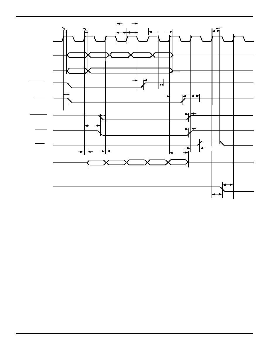
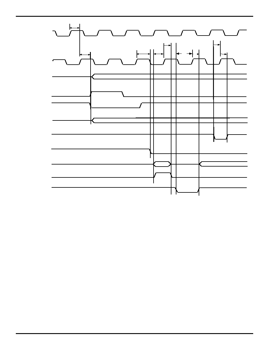
Figure 1. The ABR SAR as a PCI master (illustrates a 4-word write by the ABR SAR to host memory)
PCI_CLK
(I)
FRAME
(O)
C/
BE
3-0
(O)
AD3 1- 0
(O)
Add
Data0
Data1
Data2
Data3
C md
BE3-0
IRDY
(O)
TRDY
(I)
REQ
(O)
DEVSEL
(I)
toff
ton
tval
tval (ptp)
5350 drw 07
ParA
ParD0
ParD1
ParD2
ParD3
tcyc
tlow thigh
ton
tval
tval
tval
toff
tval
tval(ptp)
toff
ton
toff
tsu
tsu
tsu
tsu(ptp)
th
th
PAR
(O)
GNT
(I)

IDT77V252 155Mb/s ATM Segmentation & Reassembly (SAR) Controller
PRELIMINARY
with ABR for the PCI Local Bus
COMMERCIAL AND INDUSTRIAL TEMPERATURE RANGE
19
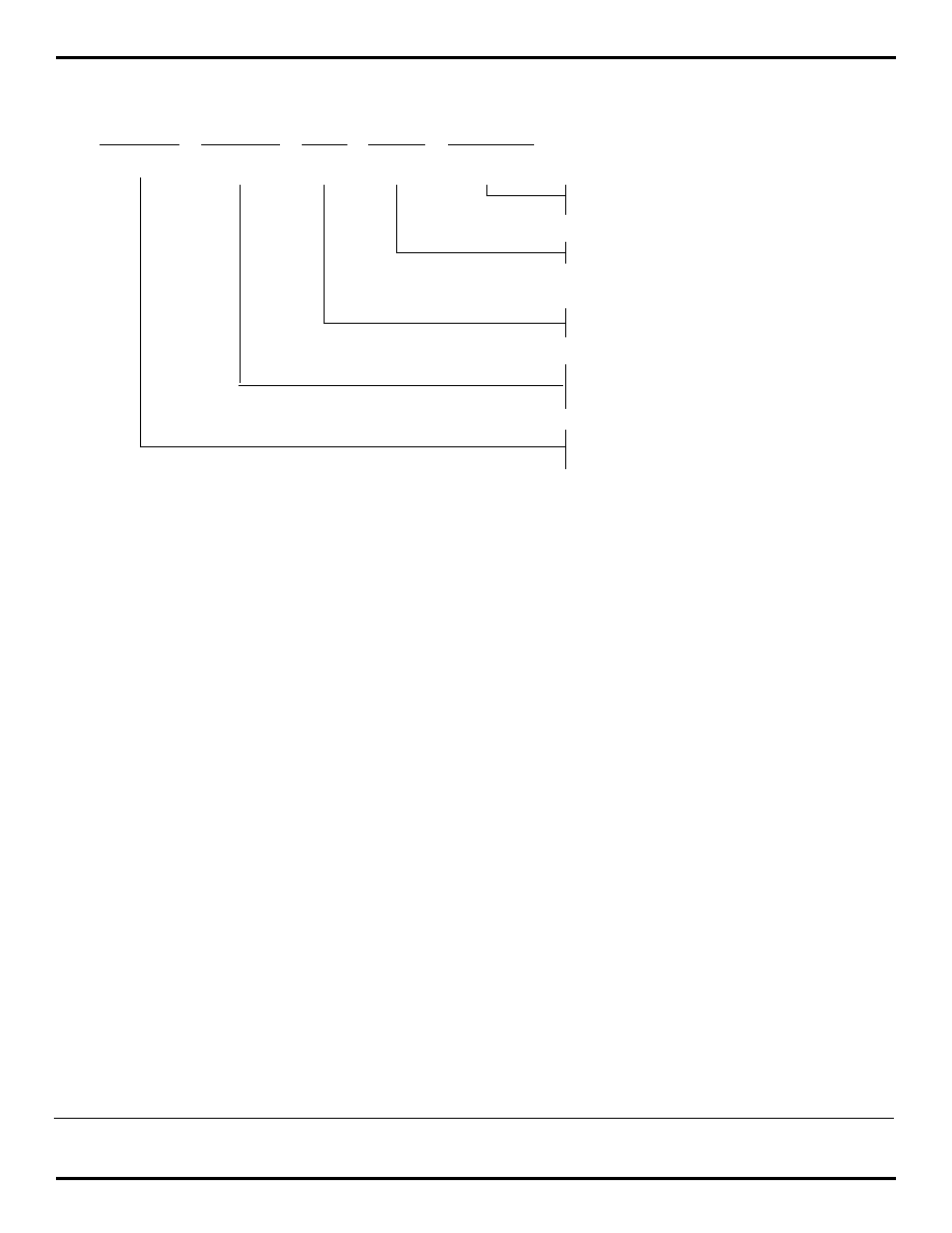
Figure 2. The ABR SAR as a PCI target
(illustrates a 4-word write operation by the host device driver to the ABR SAR )
PCI_CLK
(1)
FRAME
(1)
C/
BE
3-0
(1)
PAR
(1)
AD31-0
(1)
Add
Data0
Data1
Data2
Data3
Cmd
BE3-0
ParD0
ParD1
ParD2
ParD3
ParA
IRDY
(1)
SERR
(O)
TRDY
(O)
PERR
(O)
DEVSEL
(1)
th
tsu
5350 drw 08
tsu
tsu
tsu
th
th
th
toff
toff
toff
tval,
ton
tval,
ton
tval,
ton
tval
REQ
(1)
REQ
(O)
20
IDT77V252 155Mb/s ATM Segmentation & Reassembly (SAR) Controller
PRELIMINARY
with ABR for the PCI Local Bus
COMMERCIAL AND INDUSTRIAL TEMPERATURE RANGE
Figure 3. UTOPIA Bus Timing
P H Y _ C lk
(I)
T xD a ta 7 -0
(O )
T xC lk,R xC lk
(O )
T x S O C
(O )
T xP a rity
(O )
T x _ C trl_ In
(I)
T x _ C trl_ O u t
(O )
5350 drw 09
R x_ C trl_ O u t
(O )
R xD a ta 7 -0
(I)
R x S O C
(I)
R x _ C trl_ In
(I)
t1
t2
t5
t7
t9
t6
t8
t3
t4

IDT77V252 155Mb/s ATM Segmentation & Reassembly (SAR) Controller
PRELIMINARY
with ABR for the PCI Local Bus
COMMERCIAL AND INDUSTRIAL TEMPERATURE RANGE
21
Figure 4. Utility Bus Write Cycle
Figure 5. Utility Bus Read Cycle
UTL_CS0/1
(O)
UTL_WR
(O)
UTL_AD(7-0)
(I/O)
5350 drw 10
UTL_ALE
(O)
tw1
tw3
tw4
tw5
(O)
Valid Data
Address (O)
tw7
tw2
tw10
tw6
tw8
tw9
tw11
UTL_CS0/1
UTL_RD
UTL_AD7-0
5350 drw 11
UTL_ALE
tr1
tr3
tr4
tr5
(I)
Valid Data
Address (O)
tr7
tr2
tr8
tr10
tr9
tr2
tr11
tr6

22
IDT77V252 155Mb/s ATM Segmentation & Reassembly (SAR) Controller
PRELIMINARY
with ABR for the PCI Local Bus
COMMERCIAL AND INDUSTRIAL TEMPERATURE RANGE
SR_CS
SR_WE
SR_I/O(31-0)
5350 drw 12
t1
SR_A(18-0)
t4
t2
t5
t3
t6
SR_I/O(7-0)
5350 drw 14
SR-A (18-0)
t2
Valid Data
t4
E_CE
t1
t3
SR_CS
SR_OE
SR_I/O(31-0)
5350 drw 13
SR_A(18-0)
t1
t2
Figure 6. SRAM Bus Write Cycle Timing
Figure 7. SRAM Bus Read Cycle Timing
Figure 8. EPROM Timing

IDT77V252 155Mb/s ATM Segmentation & Reassembly (SAR) Controller
PRELIMINARY
with ABR for the PCI Local Bus
COMMERCIAL AND INDUSTRIAL TEMPERATURE RANGE
23
Several software vendors have writen IDT77V252 software drivers for various operating systems. Please contact your
local IDT sales representative for a vendor list, or e-mail atmhelp@idt.com.
IDT offers the Sarwin2 demo driver and application suite, which can be used to evaluate the IDT77V252 when used with
a IDT NIC reference or evaluation adapter. It may also be used as a reference for sample source code when developing a
proprietary device driver. Please contact your IDT sales representative or e-mail atmhelp@idt.com to obtain a free cdrom.
NIC Reference and Evaluation Adapters
NIC Reference and Evaluation adapters are available in several form factors. Bill of Materials (BOM) and schematics are
available upon request for each of the NIC adapters. A list of current NIC adapter offerings can be found at www.idt.com.
Note: The ABR SAR User Manual provides a detailed description of the 77V252 operation and registers.
SAR_CLK
EECLK
EECS
EEDI
EEDO
5350 drw 15
t1
t2
t3
Figure 9. EEPROM Timing
¥
SOFTWARE AND SOFTWARE DRIVERS
24
IDT77V252 155Mb/s ATM Segmentation & Reassembly (SAR) Controller
PRELIMINARY
with ABR for the PCI Local Bus
COMMERCIAL AND INDUSTRIAL TEMPERATURE RANGE
ORDERING INFORMATION
Notes:
Refer to PSC-4053 for detailed package drawing.
PRELIMINARY DATASHEET: DEFINITION
"PRELIMINARY" datasheets contain descriptions for products that are in early release, including features and block
diagrams.
Datasheet Document History
09/29/99:
Created New Document
01/10/00:
Changed VIH from Vcc+0.3 to 5.5V to reflect 5.5V tolerant Inputs.
03/27/00:
Corrected pins 173 and 200 in 5350drw03.
04/11/00:
Corrected table 5350tbl12.
04/26/00:
Added information in Pin Description for TxCLK and RxCLK.
06/19/00:
Corrected pin descriptions for pins 174, 189 and 199. Changed DC Operating conditions for Vil and
Vih. Updated AC Test Conditions table and drawing. Updated UTOPIA Bus, Utility Bus Read and
Write, SRAM Bus Read and Write, and EPROM timing diagrams and tables. Changed data sheet
from Advanced to Preliminary.
08/25/00:
Updated UTOPIA Bus timing table.
10/06/00:
Corrected Utopia Slave mode drawing 5351drw06 and added Max Cout parameter in Table
5350tbl09. Additional changes made to reflect Rev B silicon include changed Test[1] from pin 201 to
pin 200, changed Test[0] from pin 200 to pin 201, changed bit order for Test[1:0] in Test Mode table
5351tbl12, removed PCI timing violation for "th" hold time.
Package
IDT
NNNNN
Device Type
A
Power
NNN
Speed
A
A
Process/
Temp. Range
I
155
Speed in Mps
77V252
3.3V 155Mbs ATM Segmentation &
Reassembly (SAR) Controller for the
PCI Local Bus
Industrial
5350 drw 16
PG
208-pin Plastic Quad Flatpack
L
Low Power CMOS
(Blank)
Commercial
Integrated Device Technology, Inc.
2975 Stender Way, Santa Clara, CA 95054-3090
Telephone: (408) 727-6116
FAX 408-492-8674
Integrated Device Technology, Inc. reserves the right to make changes to the specifications in this data sheet in order to improve design or performance and to supply the best possible product.