1 of 17
April 11, 2001
2001 Integrated Device Technology, Inc.
DSC 3607/5
SwitchStar
TM
ATM Cell Based
1.2Gbps non-blocking
Integrated Switch Controller
Features
Features
Features
Features
x
Single chip controller for IDT77V400 Switching Memory
x
One IDT77V500 and one IDT77V400 form the core required
for a 1.2Gbps 8 x 8 port non-blocking switch
x
Supports up to 8192 Virtual Connections (VCs)
x
Per VC queuing for fairness, with four priorities per VC
available for each output port of the switch
x
Capable of supporting CBR, VBR, UBR, and ABR (EFCI)
service classes
x
Low power dissipation
≠ 430mW (typ.)
x
Optional header modification operation
x
Multicasting and Broadcasting capability
x
Provides congestion management support through EFCI,
CLP, and EPD functionality
x
System clock cycle times as fast as 25ns (40MHz)
x
Option available for resolving contention issues between
multiple IDT77V500 configurations
x
One IDT77V500 can manage up to eight IDT77V400's
without derating for larger switch configurations
x
Industrial temperature range (-40∞ C to +85∞ C) is available
x
Single +3.3V ± 300mV power supply
x
Available in a 100-pin Thin Plastic Quad Flat Pack (TQFP)
and 144-ball BGA
Description
Description
Description
Description
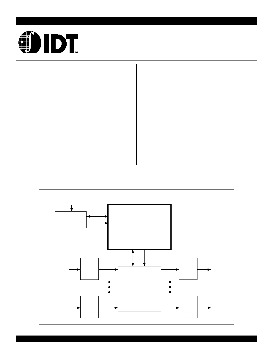
The IDT77V500 ATM Cell Based Switch Controller, when paired with
the IDT77V400 Switching Memory, forms the core control logic and
switch fabric for a 1.2Gbps non-blocking ATM switch. The IDT77V500
manages all of the switch traffic moving through the IDT77V400,
commanding the storage of incoming ATM cells and interpreting and
modifying the cell header information as necessary for data flow through
the switch. It then uses the header information, including priority indica-
tors, to queue and direct the individual cells for transmission out the
appropriate output port of the IDT77V400.
IDT77V500
Typical 8 x 8 Switch Configuration using the IDT77V500 Switch Controller
Typical 8 x 8 Switch Configuration using the IDT77V500 Switch Controller
Typical 8 x 8 Switch Configuration using the IDT77V500 Switch Controller
Typical 8 x 8 Switch Configuration using the IDT77V500 Switch Controller
SwitchStar and the IDT logo are registered trademarks of Integrated Device Technology, Inc.
8-bit Processor/
Call Setup
Manager
IDT77V500
Switch
Controller
IDT77V400
Switching
Memory
155Mbps
PHY
Port 0
Port 0
Port 7
Port 7
Control
Control
Data
Data
External Interface
for Global Setup
and Control
3607 drw 01
or IDT77V550
155Mbps
PHY
155Mbps
PHY
155Mbps
PHY
/
,
2 of 17
April 11, 2001
IDT77V500
The IDT77V500 utilizes Per Virtual Connection (VC) Queuing to keep
track of each call, and has the capacity to keep track of as many as 8192
individual VC queues. There are four possible priorities available for
each of the assigned outputs of the Switching Memory, and CBR, VBR,
UBR, and ABR-EFCI service classes are supported by the Switch
Controller. Multicasting and broadcasting services are provided,
requiring only the appropriate header information to execute these oper-
ations automatically without requiring multiple Switching Memory
entries.
The IDT77V500 also has a mode for managing and transmitting
packetized data, enabling easy transition between packet oriented
networks such as Ethernet and FDDI and ATM cell oriented networks.
The IDT77V500 has an 8-bit Manager Bus interface, MDATA0-7, to a
Call Setup Manager processor for the configuration activity and call
setup operation. When a Call Setup Cell is received by the IDT77V400,
the cell is directed to a specified output port and the payload processed
by the Call Setup Manager. The new Virtual Connection (VC) is then
established in the Queue Manager of the IDT77V500, with all operations
executed across the 8-bit Manager Bus. Subsequent cells of that partic-
ular VC are then prioritized and directed by the Switch Controller as they
are received by the IDT77V400; no further interaction with the Call
Manager processor is required for ongoing queue and cell management.
The IDT77V500 supports a major subset of the available commands
and configurations of the IDT77V400 Switching Memory. Please refer to
the SwitchStar User Manual for additional feature details and implemen-
tation information.
The IDT77V500 is fully 3.3V LVTTL compatible, and is packaged in
an 100-pin Thin Plastic Quad Flatpack (TQFP) and an 144-ball BGA.
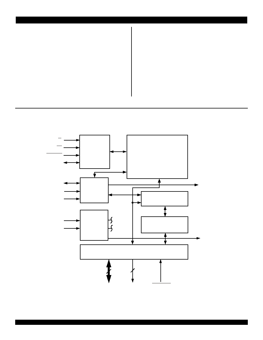
Functional Block Diagram
Functional Block Diagram
Functional Block Diagram
Functional Block Diagram
1
SCLK and Reset are inputs to all blocks.
2
Outputs are always enabled (active).
IOD0-31
32
Control
Logic
OFRM0-7
CRCERR
SCLK
CMD0-5
6
3607 drw 02
Call
Setup
Manager
MDATA0-7
MSTRB
MD/C
MR/W
Switching Memory Interface
Output
Service
and
Arbitration
State
Machine
Queue Manager
Output Queues
and
Link Registers
RESETI
RESETO
CBRCLK2
CBRCLK3
SFRM
Reset
1
SCLK
1
2
2
2

3 of 17
April 11, 2001
IDT77V500
Package Diagrams
Package Diagrams
Package Diagrams
Package Diagrams
All Vcc pins must be connected to power supply. All Vss pins must be connected to ground supply.
1
This package code is used to reference the package diagram.
2
This text does not indicate orientation of the actual part marking.
100 99 98 97 96 95 94 93 92 91 90 89 88 87 86 85 84 83 82 81 80 79 78 77 76
I
O
D
5
I
O
D
4
V
S
S
V
C
C
I
O
D
3
I
O
D
2
I
O
D
1
C
R
C
E
R
R
V
C
C
M
D
A
T
A
0
M
D
A
T
A
1
M
D
A
T
A
2
V
C
C
V
S
S
M
D
A
T
A
5
M
D
A
T
A
6
M
D
A
T
A
3
M
D
A
T
A
4
N
C
N
C
N
C
Index
1
2
3
4
5
6
7
8
9
10
11
12
13
14
15
16
17
18
19
20
21
22
23
24
25
NC
NC
RESETI
NC
NC
NC
CMD3
MSTRB
MR/W
NC
CMD4
CMD5
V
C
C
I
O
D
2
4
N
C
N
C
75
74
73
72
71
70
69
68
67
66
65
64
63
62
61
60
59
58
57
56
55
54
53
52
51
NC
IOD
13
V
CC
V
SS
IOD
11
IOD
10
IOD
9
IOD
8
IOD
7
NC
NC
IOD
12
26 27 28 29 30 31 32 33 34 35 36 37 38 39 40 41 42 43 44 45 46 47 48 49 50
IDT77V500PF
PN100-1
1
100-Pin TQFP
Top View
2
3607 drw 03
V
C
C
V
C
C
I
O
D
0
I
O
D
6
IOD
14
IOD
15
IOD
16
IOD
17
IOD
18
IOD
19
NC
V
SS
V
CC
IOD
20
IOD
21
IOD
22
IOD
23
N
C
V
S
S
I
O
D
2
5
I
O
D
2
6
I
O
D
2
7
I
O
D
2
8
I
O
D
2
9
I
O
D
3
0
I
O
D
3
1
V
S
S
V
S
S
V
S
S
V
C
C
V
S
S
O
F
R
M
0
O
F
R
M
1
O
F
R
M
2
O
F
R
M
3
O
F
R
M
4
O
F
R
M
5
O
F
R
M
6
MDATA
7
MD/C
V
CC
V
SS
CMD2
CMD1
CMD0
RESETO
SCLK
CBRCLK2
CBRCLK3
SFRM
OFRM7
,

4 of 17
April 11, 2001
IDT77V500
BGA Package Diagram
BGA Package Diagram
BGA Package Diagram
BGA Package Diagram
VCC
OFRM4
NC
OFRM7 CBRCLK2
SCLK
NC
VCC
CMD4
NC
MDATA7
NC
VSS
OFRM3
OFRM2
NC
CBRCLK3 RESETO
RESETI
VSS
CMD5
MSTRB
MD/C
MDATA6
NC
NC
NC
OFRM5
SFRM
NC
NC
CMD1
CMD3
MR/W
MDATA5
NC
NC
NC
NC
OFRM1
OFRM6
NC
NC
CMD0
NC
NC
VSS
MDATA4
NC
NC
NC
NC
OFRM0
VCC
NC
NC
MDATA3
MDATA1
NC
NC
VSS
NC
VSS
NC
NC
CMD2
VCC
MDATA2 MDATA0
NC
NC
VCC
NC
VSS
NC
IOD28
IOD19
CRCERR
VCC
NC
NC
NC
NC
IOD31
NC
IOD30
IOD27
VCC
IOD12
IOD8
VCC
NC
NC
NC
NC
IOD29
VSS
NC
IOD24
IOD17
IOD14
VCC
IOD6
NC
IOD0
NC
IOD1
NC
IOD25
IOD26
IOD20
NC
IOD15
IOD13
VSS
VCC
IOD3
IOD2
NC
NC
IOD22
NC
VSS
NC
NC
NC
IOD10
IOD7
NC
VSS
IOD4
NC
IOD23
NC
IOD21
IOD18
IOD16
NC
IOD11
IOD9
NC
NC
IOD5
1
3
2
4
5
6
7
8
9
10
11
12
A
B
C
D
E
F
G
H
J
K
L
M
A
B
C
D
E
F
G
H
J
K
L
M
1
3
2
4
5
6
7
8
9
10
11
12
NC
5 of 17
April 11, 2001
IDT77V500
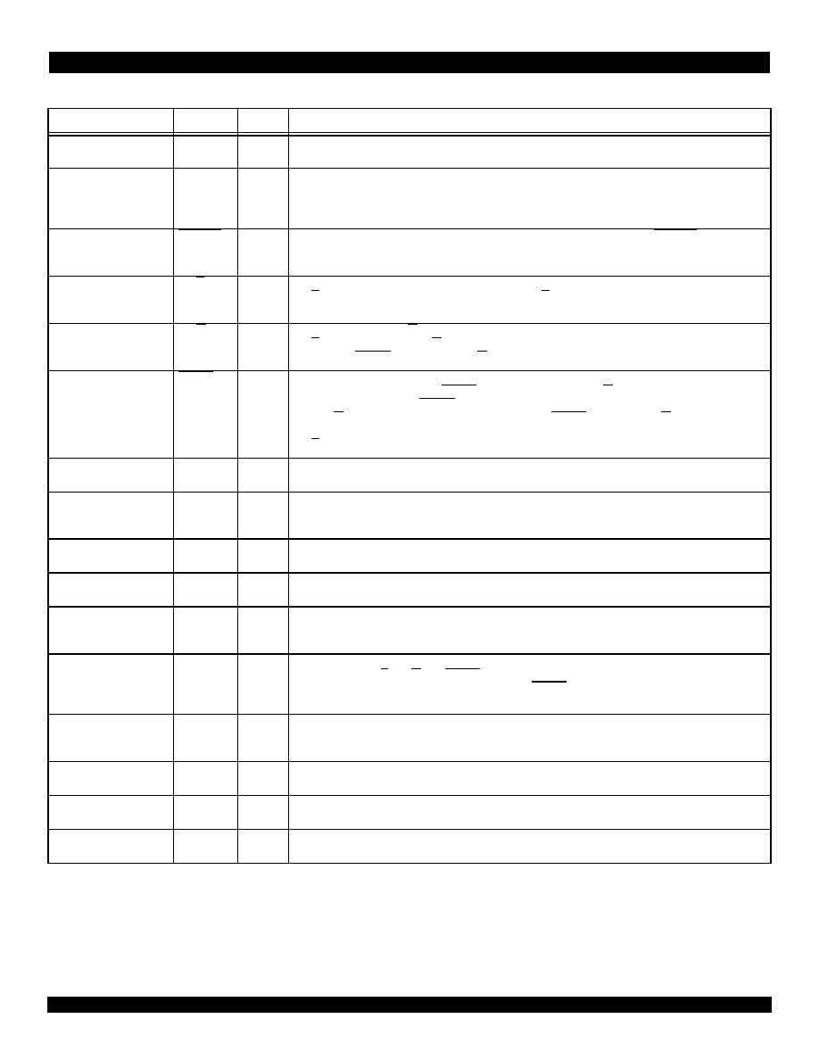
TQFP Pin Description
TQFP Pin Description
TQFP Pin Description
TQFP Pin Description
Pin Number
Symbol
Type
Description
18
SCLK
I
System clock: Reference clock input for all synchronous pins of the IDT77V500 Switch Controller. All synchro-
nous signals are referenced to the rising edge of SCLK.
22,20
CBRCLK3,
CBRCLK2
I
CBR Clocks 3 and 2: External clock signals used when Constant Bit Rate (CBR) Service classes are utilized.
These clock signals correspond to Output Port priorities 3 and 2 respectively and are used to determine the
constant bit rate for the controller. Priority 3 is the highest priority. If CBR mode is not used these pins should
be pulled up to Vcc with a resistor with a recommended value of 5K ohm or less.
86
CRCERR
I
Cyclical Redundancy Check Error: Synchronous input on the rising edge of SCLK. CRCERR asserted LOW
by the IDT77V400 Switching Memory during a store operation indicates that a HEC CRC error has occurred in
the cell header.
2
MD/C
I
Manager Control: Selects the data or control registers of the IDT77V500 for the Manager Bus Operation.
MD/C asserted HIGH selects the data registers, and MD/C LOW selects the command/status registers of the
IDT77V500.
3
MR/W
I
Manager Read/Write: MR/W LOW will write the data on the Manager Bus into the registers selected by the
MD/C input. In write mode (MR/W LOW) the data on MDATA0-7 is written synchronously with respect to the
rising edge of MSTRB; in read mode (MR/W HIGH) the data is accessed asynchronously.
4
MSTRB
I
Manager Strobe: Input which acts as a clock for the Manager Bus (MDATA0-7). Other Manager Bus inputs are
synchronous to the rising edge of MSTRB during write operations (MR/W LOW) and must meet the specified
Setup and Hold parameters. MSTRB performs an asynchronous Output Enable function when a read opera-
tion (MR/W HIGH) is executed on the Manager Bus. When MSTRB is LOW and MR/W is HIGH (Read Mode)
the Manager Bus is enabled in output mode and the contents of the IDT77V500 registers (determined by the
MD/C input) are available to be read on MDATA0-7.
17
RESETI
I
Reset Input: When asserted HIGH, this signal asynchronously initiates the internal reset sequence of the
IDT77V500.
19
RESETO
O
Reset Output: Asserted HIGH upon initiating the reset of the IDT77V500 (RESETI HIGH). In multiple
IDT77V500 configurations, this output is connected to the RESETI input of the next controller in the chain.
RESETO will remain HIGH until a START command is received from the Call Setup Manager.
7-9, 12-14
CMD0-5
O
Command Bus: Synchronized with SCLK, instructions to be executed by the IDT77V400 Switching memory
are output by the IDT77V500 on this 6-bit bus.
24
SFRM
O
Synchronize Output Frame: Synchronous output used when multiple IDT77V500's contend for a common bus.
The Master IDT77V500 generates this signal which then drives the OFRM0 input of the other IDT77V500s.
40-43, 46-49, 53-56, 59-66,
69-73, 77-79, 82-85
IOD0-31
I/O
Control Data Bus: Synchronous with SCLK and one cycle latent to the Command Bus (CMD0-5). Used for
transfer of the header bytes, configuration register, error and status registers, and the cell memory address
between the IDT77V500 and the IDT77V400 Switching Memory.
1, 90-93, 96-98
MDATA0-7
I/O
Manager Bus: Communications between the Call Setup Manager and the IDT77V500 occur over this 8-bit bi-
directional bus. MD/C, MR/W, and MSTRB determine the mode and data type transferred across the MDATA
bus. Write operations are synchronous with respect to MSTRB, while MDATA behaves asynchronously for
read operations.
25, 28-29, 32-35, 36
OFRM1-7
OFRM0
I/O
Output Frame: Asynchronous input pins used by the IDT77V500 to detect when the next cell can be loaded to
the specified IDT77V400 output port 0 through 7. When in multiple IDT77V500 configurations, the OFRM1-7
are redefined as CBUS1-7 for arbitration. OFRM0 is always an input pin (There is no CBUS0).
11, 31, 45, 58, 68, 81, 87-
89, 94
VCC
Power
Power Supply (+3.3V ±300mV)
10, 30, 37-39, 44, 57, 67,
80, 95
VSS
Power
Ground
5-6, 15-16, 21, 23, 26-27,
50-52, 74-76, 99-100
NC
____
No Connect

6 of 17
April 11, 2001
IDT77V500
BGA Pin Description
BGA Pin Description
BGA Pin Description
BGA Pin Description
Pin Number
Symbol
Type
Description
A6
SCLK
I
System clock: Reference clock input for all synchronous pins of the IDT77V500 Switch Controller. All synchro-
nous signals are referenced to the rising edge of SCLK.
B5, A5
CBRCLK3,
CBRCLK2
I
CBR Clocks 3 and 2: External clock signals used when Constant Bit Rate (CBR) Service classes are utilized.
These clock signals correspond to Output Port priorities 3 and 2 respectively and are used to determine the
constant bit rate for the controller. Priority 3 is the highest priority. If CBR mode is not used these pins should
be pulled up to Vcc with a resistor with a recommended value of 5K ohm or less.
G7
CRCERR
I
Cyclical Redundancy Check Error: Synchronous input on the rising edge of SCLK. CRCERR asserted LOW
by the IDT77V400 Switching Memory during a store operation indicates that a HEC CRC error has occurred in
the cell header.
B11
MD/C
I
Manager Control: Selects the data or control registers of the IDT77V500 for the Manager Bus Operation.
MD/C asserted HIGH selects the data registers, and MD/C LOW selects the command/status registers of the
IDT77V500.
C10
MR/W
I
Manager Read/Write: MR/W LOW will write the data on the Manager Bus into the registers selected by the
MD/C input. In write mode (MR/W LOW) the data on MDATA0-7 is written synchronously with respect to the
rising edge of MSTRB; in read mode (MR/W HIGH) the data is accessed asynchronously.
B10
MSTRB
I
Manager Strobe: Input which acts as a clock for the Manager Bus (MDATA0-7). Other Manager Bus inputs are
synchronous to the rising edge of MSTRB during write operations (MR/W LOW) and must meet the specified
Setup and Hold parameters. MSTRB performs an asynchronous Output Enable function when a read opera-
tion (MR/W HIGH) is executed on the Manager Bus. When MSTRB is LOW and MR/W is HIGH (Read Mode)
the Manager Bus is enabled in output mode and the contents of the IDT77V500 registers (determined by the
MD/C input) are available to be read on MDATA0-7.
B7
RESETI
I
Reset Input: When asserted HIGH, this signal asynchronously initiates the internal reset sequence of the
IDT77V500.
B6
RESETO
O
Reset Output: Asserted HIGH upon initiating the reset of the IDT77V500 (RESETI HIGH). In multiple
IDT77V500 configurations, this output is connected to the RESETI input of the next controller in the chain.
RESETO will remain HIGH until a START command is received from the Call Setup Manager.
D8, C8, F7, C9, A9, B9
CMD0-5
O
Command Bus: Synchronized with SCLK, instructions to be executed by the IDT77V400 Switching memory
are output by the IDT77V500 on this 6-bit bus.
C5
SFRM
O
Synchronize Output Frame: Synchronous output used when multiple IDT77V500's contend for a common bus.
The Master IDT77V500 generates this signal which then drives the OFRM0 input of the other IDT77V500s.
J10, J12, K11, K10, L12,
M12, J8, L9, H7, M9, L8,
M8, H6, K7, J6, K6, M6, J5,
M5, G6, K4, M4, L3, M3, J4,
K3, K2, H4, G5, J1, H2, H1
IOD0-31
I/O
Control Data Bus: Synchronous with SCLK and one cycle latent to the Command Bus (CMD0-5). Used for
transfer of the header bytes, configuration register, error and status registers, and the cell memory address
between the IDT77V500 and the IDT77V400 Switching Memory.
F10, E11, F9, E10, D12,
C11, B12, A11
MDATA0-7
I/O
Manager Bus: Communications between the Call Setup Manager and the IDT77V500 occur over this 8-bit bi-
directional bus. MD/C, MR/W, and MSTRB determine the mode and data type transferred across the MDATA
bus. Write operations are synchronous with respect to MSTRB, while MDATA behaves asynchronously for
read operations.
D4, B2, B3, A3, C4, D5,
A4, E5
OFRM1-7
OFRM0
I/O
Output Frame: Asynchronous input pins used by the IDT77V500 to detect when the next cell can be loaded to
the specified IDT77V400 output port 0 through 7. When in multiple IDT77V500 configurations, the OFRM1-7
are redefined as CBUS1-7 for arbitration. OFRM0 is always an input pin (There is no CBUS0).
A1, A8, E6, F8, G1, G8,
H5, H8, J7, K9
VCC
Power
Power Supply (+3.3V ±300mV)
B1, B8, D11, F3, F4, G2,
J3, K8, L4, L11
VSS
Power
Ground
A2, A7, A10, A12, B4, C1,
C2, C3, C6, C7, C12, D1,
D2, D3, D6, D7, D9, D10,
E1, E2, E3, E4, E7, E8, E9,
E12, F1, F2, F5, F6, F11,
F12, G3, G4, G9, G10,
G11, G12, H3, H9, H10,
H11, H12, J2, J9, J11, K1,
K5, K12, L1, L2, L5, L6, L7,
L10, M1, M2, M7, M10, M11
NC
____
No Connect
7 of 17
April 11, 2001
IDT77V500
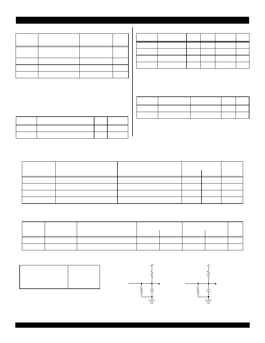
Absolute Maximum Ratings
Absolute Maximum Ratings
Absolute Maximum Ratings
Absolute Maximum Ratings
Maximum Operating Temperature and Supply
Maximum Operating Temperature and Supply
Maximum Operating Temperature and Supply
Maximum Operating Temperature and Supply
Voltage
Voltage
Voltage
Voltage
Symbol
Rating
1
1.
Stresses greater than those listed in this table may cause permanent damage to the device.
This is a stress rating only and functional operation of the device at these or any other con-
ditions above those indicated in the operational sections of this specification is not implied.
Exposure to absolute maximum rating conditions for extended periods may affect reliability.
Commercial &
Industrial
Unit
V
TERM2
2.
V
TERM
must not exceed Vcc + 0.3V for more than 25% of the cycle time or 10ns maxi-
mum, and is limited to
20mA for the period of V
TERM
Vcc + 0.3V.
Terminal Voltage with
Respect to GND
-0.5 to +3.9
V
T
BIAS
Temperature Under Bias
-55 to +125
∞
C
T
STG
Storage Temperature
-55 to +125
∞
C
I
OUT
DC Output Current
50
mA
Grade
Ambient Temperature
1
1.
This is the parameter T
A
.
GND
Vcc
Commercial 0
∞
C to +70
∞
C
0V
3.3V ± 0.3V
Industrial
-40
∞
C to +85
∞
C
0V
3.3V ± 0.3V
Recommended DC Operating Conditions
Recommended DC Operating Conditions
Recommended DC Operating Conditions
Recommended DC Operating Conditions
Capacitance (T
Capacitance (T
Capacitance (T
Capacitance (T
A
A
A
A
= +25∞C, f = 1.0MH
= +25∞C, f = 1.0MH
= +25∞C, f = 1.0MH
= +25∞C, f = 1.0MH
z
z
z
z
) TQFP Only
) TQFP Only
) TQFP Only
) TQFP Only
Symbol
Parameter
Min. Typ.
Max.
Unit
V
CC
Supply Voltage
3.0
3.3
3.6
V
V
SS
Ground
0
0
0
V
V
IH
Input High Voltage 2.0
____
V
CC
+0.3V
1, 2
1.
V
TERM
must not exceed Vcc + 0.3V or Vss ≠ 0.3V.
2.
V
TERM
must not exceed Vcc + 0.3V for more than 25% of the cycle time or 10ns maxi-
mum, and is limited to
20mA for the period of V
TERM
Vcc + 0.3V.
V
V
IL
Input Low Voltage -0.5
1,3
3.
V
IL
-1.5V for pulse width less than 10ns.
____
0.8
V
Symbol
Parameter
1
1.
These parameters are determined by device characterization, but are not production test-
ed.
Conditions
2
2.
3dV references the interpolated capacitance when the input and output switch from 0V
to 3V or from 3V to 0V.
Max. Unit
C
IN
Input Capacitance
V
IN
= 3dV
9
pF
C
OUT3
3.
C
OUT
also references C
I/O
.
Output Capacitance V
OUT
= 3dV
10
pF
DC Electrical Characteristics Over the Operating Temperature and Supply Voltage Range
DC Electrical Characteristics Over the Operating Temperature and Supply Voltage Range
DC Electrical Characteristics Over the Operating Temperature and Supply Voltage Range
DC Electrical Characteristics Over the Operating Temperature and Supply Voltage Range
(Vcc = 3.3V ± 0.3V)
(Vcc = 3.3V ± 0.3V)
(Vcc = 3.3V ± 0.3V)
(Vcc = 3.3V ± 0.3V)
DC Electrical Characteristics Over the Operating Temperature and Supply Voltage Range
DC Electrical Characteristics Over the Operating Temperature and Supply Voltage Range
DC Electrical Characteristics Over the Operating Temperature and Supply Voltage Range
DC Electrical Characteristics Over the Operating Temperature and Supply Voltage Range
(V
(V
(V
(V
CC
CC
CC
CC
= 3.3V ± 0.3V)
= 3.3V ± 0.3V)
= 3.3V ± 0.3V)
= 3.3V ± 0.3V)
AC Test Conditions
AC Test Conditions
AC Test Conditions
AC Test Conditions
Symbol
Parameter
Test Conditions
77V500S
Unit
Min
Max
|I
LI
|
Input Leakage Current
Vcc = 3.6V, V
IN
= 0V to Vcc
___
10
µA
|I
LO
|
1
1.
For MDATA, IOD, and OFRM pins only.
Output Leakage Current
RESETI = V
IH
, V
OUT
= 0V to Vcc
___
10
µA
V
OL
Output Low Voltage
I
OL
= +4mA
___
0.4
V
V
OH
Output High Voltage
I
OH
= -4mA
2.4
___
V
Symbol
Parameter
Test Conditions
77V500S25PFI
77V500S25PF
Unit
Min
Max
Min
Max
I
CC
Operating Current
Vcc = 3.6V, RESETI = V
IL,
f = f
MAX1
1.
At f = fmax SCLK is cycling at maximum frequency and all inputs are cycling at 1/tCYC1, using AC input levels of VSS to 3.0V.
130
200
130
175
mA
I
CCR
Reset Current
Vcc = 3.6V, RESETI = V
IH,
f = f
MAX1
150
325
150
300
mA
Input Pulse Levels
Input Rise/Fall Times
Input Timing Reference Levels
Output Reference Levels
Output Load
VSS to 3.0V
3ns Max.
1.5V
1.5V
Figures 1 and 2
Figure 1 AC Output Test Load
Figure 2 Output Test Load
(for High-Impedance parameters) *Including scope and jig.
590
50pF
435
DATA
OUT
590
5pF*
435
DATA
OUT
3607 drw 04
3607 drw 05
3.3V
3.3V

8 of 17
April 11, 2001
IDT77V500
AC Electrical Characteristics Over the Operating Temperature Range
AC Electrical Characteristics Over the Operating Temperature Range
AC Electrical Characteristics Over the Operating Temperature Range
AC Electrical Characteristics Over the Operating Temperature Range
(Vcc = 3.3V ± 0.3V)
(Vcc = 3.3V ± 0.3V)
(Vcc = 3.3V ± 0.3V)
(Vcc = 3.3V ± 0.3V)
Symbol
Parameter
77V500S25 Com'l & Ind
Unit
Min.
Max.
t
CYC
System Clock Cycle Time
25
--
ns
t
CH
System Clock High Time
10
--
ns
t
CL
System Clock Low Time
10
--
ns
t
R
Clock Rise Time
--
3
ns
t
F
Clock Fall Time
--
3
ns
t
MCYC
Manager Clock Cycle Time
25
--
ns
t
MCH
Manager Clock High Time
6
--
ns
t
MCL
Manager Clock Low Time
19
--
ns
t
SM
MD/C Setup Time to MSTRB High
10
--
ns
t
HM
MD/C Hold Time after MSTRB High
2
--
ns
t
SMRW
MR/W Setup Time to MSTRB High
10
--
ns
t
HMRW
MR/W Hold Time after MSTRB High
2
--
ns
t
SMD
MDATA Setup Time to MSTRB High
10
--
ns
t
HMD
MDATA Hold Time after MSTRB High
2
--
ns
t
SCRC
CRCERR Setup Time to SCLK High
5
--
ns
t
HCRC
CRCERR Hold Time after SCLK High
2
--
ns
t
SIO
IOD Setup Time to SCLK High
5
--
ns
t
HIO
IOD Hold Time after SCLK High
2
--
ns
t
OFP
OFRM High Pulse Width
5
--
ns
t
CDC
SCLK to CMD Valid
--
18
ns
t
DCC
CMD Output Hold after SCLK High
2
--
ns
t
CDS
SCLK to SFRM Valid
--
18
ns
t
DCS
SFRM Output Hold after SCLK High
2
--
ns
t
CDIO
SCLK to IOD Valid
--
18
ns
t
DCIO
IOD Output Hold after SCLK High
2
--
ns
t
AMD
MSTRB Low to MDATA Valid
--
18
ns
t
OHMD
MDATA Output Hold after MSTRB High
2
--
ns
t
CDOF
SCLK to OFRM/CBUS Valid
--
18
ns
t
DCOF
OFRM/CBUS Output Hold after SCLK High
2
--
ns
t
RSI
RESETI High Pulse Width
1
1.
RESETI must be held High for 8 SCLK cycles. After RESETI transitions Low, 8191 cycles are required before the Status Acknowledge bits will
indicate that the internal reset process in complete.
8
--
t
CYC
t
RSO
RESETO High after RESETI High
--
2
t
CYC
t
CDR
SCLK to RESETO Valid
--
18
ns
t
CKHZ
SCLK High to Output High-Z
2
2.
Transition is measured +/-200mV from Low or High impedance voltage with the Output Test Load (Figure 2). This parameter is guaranteed by
device characterization, but is not production tested.
--
10
ns
t
CKLZ
SCLK High to Output Low-Z
2
2
--
ns
t
CYC3
CBRCLK3 Clock Cycle Time
3
3.
Cycle units insure that the SCLK recognizes the state of CBRCLK.
3
--
t
CYC
t
CH3
CBRCLK3 Clock High Time
3
1.2
--
t
CYC
t
CL3
CBRCLK3 Clock Low Time
3
1.2
--
t
CYC
t
CYC2
CBRCLK2 Clock Cycle Time
3
3
--
t
CYC
t
CH2
CBRCLK2 Clock High Time
3
1.2
--
t
CYC
t
CL2
CBRCLK2 Clock Low Time
3
1.2
--
t
CYC
9 of 17
April 11, 2001
IDT77V500
Control Interface Timing Waveform
Control Interface Timing Waveform
Control Interface Timing Waveform
Control Interface Timing Waveform
This waveform describes the command interaction across the IOD Bus to the IDT77V400 Switching Memory.
1
The result of this GET STATUS command is that an ISAM is full and ready to be stored to the Cell Memory of the IDT77V400.
Control Interface Commands
Control Interface Commands
Control Interface Commands
Control Interface Commands
(1)
(1)
(1)
(1)
SFRM, CBUS, and OFRM Timing Waveforms
SFRM, CBUS, and OFRM Timing Waveforms
SFRM, CBUS, and OFRM Timing Waveforms
SFRM, CBUS, and OFRM Timing Waveforms
1
OFRM1-7 become CBUS1-7 (Outputs) during cell bus operations to arbitrate between multiple IDT77V500's.
Command
1
1.
CMD bus commands not defined in this table are undefined and are not implemented by the IDT77V500.
Command Description
Command Bus Bit (CMD5:0)
MSb
LSb
5
4
3
2
1
0
GHIx
Get Header from ISAMx
2
2.
"x" represents the specific ISAM or OSAM being accessed (IP0-IP7 or OP0-OP7 respectively).
0
0
1
n
3
3.
"n" represents the appropriate bit of the binary representation of the ISAM or OSAM being accessed (000 to 111).
n
3
n
3
GST
Get ISAM Status Register Bits
0
1
0
0
1
0
GER
Get Error Register Bits
0
1
0
1
1
0
STEx
Store Cell in ISAMx
2
and Edit Buffer in Memory
1
0
0
n
3
n
3
n
3
LDOx
Load Cell from Memory into OSAMx
2
1
1
0
n
3
n
3
n
3
PHE
Put new Header in Edit Buffer
1
1
1
1
0
0
PHEC
Put new Header and new CRC byte in Edit Buffer
1
1
1
1
0
1
REF
Refresh Cell Memory
0
1
0
1
1
1
LDC
Load Configuration Register
1
1
1
0
1
0
OHE
Put new Header in Output Edit Register
1
1
1
1
1
0
OHEC
Put new Header and new CRC byte in Output Edit Register
1
1
1
0
0
1
GET
STATUS
STORE
ISAM
PUT
HEADER
GET
HEADER ISAM
GET
STATUS
SCLK
CRCERR
3607 drw 06
CMD0-5
IOD0-31
Input -
Old Header
[ CRC ERROR = LOW ]
Output -
New Header
[ AVAILABLE FOR NEXT COMMAND ]
Output -
Cell Addr
t
CYC
t
CH
t
CL
t
CDC
t
DCC
t
SIO
t
SCRC
t
HCRC
t
CDIO
t
DCIO
STATUS
STATUS
1
t
HIO
1
t
CDIO
t
DCIO
SCLK
OFRM
3607 drw 07
t
OFP
OFRM/CBUS
t
CDOF
t
DCOF
1
SFRM
t
DCS
t
CDS
10 of 17
April 11, 2001
IDT77V500
Manager Commands
Manager Commands
Manager Commands
Manager Commands
Manager Bus Read Timing Waveform
Manager Bus Read Timing Waveform
Manager Bus Read Timing Waveform
Manager Bus Read Timing Waveform
Write operations, both for Commands and Data, are synchronous to the rising edge of MSTRB. The data placed on the MDATA pins is determined
by the state of the MD/C pin.
1
The combination of MSTRB Low and MR/W High (Read mode) asynchronously enables the MDATA pins as outputs. That is, data is available to be read one asynchronous tAMD time
after the falling edge of MSTRB if MR/W is High.
2
After the Command is written, the Manager must take MR/W High (Read mode) to wait for a valid Command Acknowledge from the IDT77V500 before proceeding. Reading a High
Bit 7 of the status register under these conditions indicates the command has been acknowledged by the IDT77V500. This may take multiple IDT77V500 SCLK cycles based on possible
higher priority operations that the IDT77V500 must support.
3
A valid Acknowledge from the IDT77V500 is indicated by a High Command Acknowledge bit (Bit 7 of the Status Register).
4
Waveform illustrates first two bytes of data only. Additional bytes may be available based on command used.
Manager Bus Write Timing Waveform
Manager Bus Write Timing Waveform
Manager Bus Write Timing Waveform
Manager Bus Write Timing Waveform
Write operations, both for Commands and Data, are synchronous to the rising edge of MSTRB. The data placed on the MDATA pins is determined
by the state of the MD/C pin.
1
Either a Read cycle was completed or a Status Acknowledge was executed immediately prior to the first MSTRB of this write waveform.
2
The combination of MSTRB Low and MR/W High (Read mode) asynchronously enables the MDATA pins as outputs. The data placed on the MDATA pins is determined by the state
of the MD/C pin.
3
After the Command is written, the Manager must take MR/W High (Read mode) to wait for a valid Command Acknowledge from the IDT77V500 before proceeding. Reading a High
Bit 7 of the status register under these conditions indicates the command has been acknowledged by the IDT77V500. This may take multiple IDT77V500 SCLK cycles based on possible
higher priority operations that the IDT77V500 must support.
4
A valid Acknowledge from the IDT77V500 is indicated by a High Command Acknowledge bit (Bit 7 of the Status Register).
Command
1
1.
Manager Command codes not defined in this table are not to be used.
Command Name
Command Description
Code (in Hex)
WRSL
Write Service Link Memory
Write into Service Link Memory to initialize scheduled service lists.
03
STAT
Read IDT77V500 status
Reads the internal status of the IDT77V500. Available information includes various
error registers and counts.
07
LDCFG
Load IDT77V400 Configuration Bits Passes configuration information to the IDT77V400.
08
SUP
Call setup
Writes the appropriate information into an entry of the Per VC Memory to perform the
call setup function.
09
INT
Initialize IDT77V500
Initializes the internal configuration registers of the IDT77V500.
0A
SEL
Select a IDT77V500
Selects the IDT77V500 to be enabled in a multiple device configuration.
0B
START
End of IDT77V500 Initialization
Sets the IDT77V500 into an enabled state after it has been initialized.
0C
CBR
Set up a CBR Scheduler
Sets up a selected output service list in the Constant Bit Rate (CBR) mode.
0D
PARM
Set Parameters
Sets various parameters in the IDT77V500, including the CLP low water mark, the
EFCI low water mark, and the EPD low water mark.
0E
MD/
C
M S TR B
MR/
W
3607 drw 08
t
SMRW
t
HMRW
t
SMD
t
HMD
MDATA
t
MCH
t
MCL
t
MCYC
t
SM
t
HM
Write first
8 ADDR bits
Acknowledge Read
t
AMD
DATA
OUT
DATA
OUT
CMD
IN
ADDR
IN
ADDR
IN
t
OHMD
Write last
8 ADDR bits
Write Cycle-
Read Command
1
2
DATA
OUT
DATA
OUT
DATA
OUT
3
Read Byte 0
Acknowledge Read
Acknowledge Read ≠
Valid Command Acknowledge
t
AMD
t
OHMD
t
SMRW
t
SM
Read Byte 1
4
MDATA
M S TR B
t
SM
t
HM
3607 drw 09
t
SMRW
t
HMRW
t
SMD
t
HMD
MR/
W
MD/
C
t
MCH
t
MCL
t
MCYC
DATA
IN
DATA
IN
CMD
IN
DATA
OUT
Write Data Byte 0
Write Data Byte 12
Write Cycle-
Write Command
Acknowledge Read
t
OHMD
T0
T12
t
AMD
DATA
OUT
2
3
Acknowledge Read
DATA
OUT
DATA
OUT
4
Acknowledge Read
Acknowledge Read ≠
Valid Command Acknowledge
t
SM
t
SMRW
1

11 of 17
April 11, 2001
IDT77V500
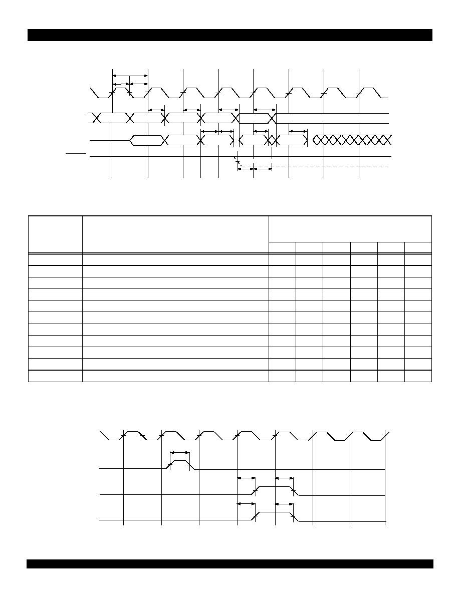
CBR Clock Parameters
CBR Clock Parameters
CBR Clock Parameters
CBR Clock Parameters
"x" for this waveform represents either 2 or 3, depending on which CBRCLK is used (CBRCLK2 or CBRCLK3).
CBRCLKx
t
CLx
t
CHx
t
CYCx
3607 drw 11
the pointer should be moved back to the top of the CBR VC List if all the
VCs in the list have been serviced. Thus the user can establish a frame
duration and be assured that a cell from each VC in the OPyCBRx VC
List is transmitted in each frame time. Sub lists can also be established
within the CBR VC List so that a particular VC could be weighted to ship
more cells per frame than the others.
Example 2 illustrates using very slow CBR clocks (tCHx greater than
or equal to 8 SCLKs) to shape traffic in a VBR form of implementation. A
cell from a VC on the OPyCBRx VC List is again scheduled on each
rising clock edge of SCLK after a falling edge of CBRCLKx, but since
t
CH
x is HIGH for more than eight SCLKs, there is more direct control
over the exact time in which each cell of the VC List is scheduled. The
single cell will then be transmitted when the output is available and other
previously scheduled Input and Output ports of the IDT77V400 have
been serviced (there is again the potential delay based on other traffic
passing through the IDT77V400). The IDT77V500 will service all of the
VCs in the OPyCBRx VC List because the count will prevent the pointer
from returning to the top of the CBR VC List until all VCs on the list with
cells have been serviced. The user can thus more closely manage the
transmission of cells with this slower CBR clock rate because it is more
directly related to individual CBRCLKx High-to-Low transitions.
Figure 3 OPyBRx VC Example
3607 drw 10
100
200
300
400
Beginning
End
CBR Functional Description
CBR Functional Description
CBR Functional Description
CBR Functional Description
The Constant Bit Rate (CBR) functionality of the IDT77V500 provides
both the opportunity for scheduling priority traffic at a regular interval and
traffic shaping capability. Two external CBR clocks, CBRCLK3 and
CBRCLK2, are available and associated with Output Priority 3 (Highest
Priority) and Priority 2 respectively. Calls assigned to a particular CBR
VC in the IDT77V500 Per VC Table are linked together in a CBR Per VC
list by output, so that a cell from each VC of a particular CBR Per VC list
are serviced on each cycle through the list. The CBR Per VC List is iden-
tified by both the output and CBR priority on that output; for example,
OPyCBRx VC list represents Output y (Output number 0-7) and CBR
priority x (CBR priority 3 or 2). Figure 3 is an example of an OPyCBRx
VC List with four VCs in the list: 100 (the first entry in the list), 200, 300
and 400. The arrows indicate the linking sequence in this VC List. Figure
3 will be used with the CBR Clock Functional Waveforms to illustrate two
basic functional implementations using the CBR Clocks.
CBR Clock Functional Waveform Example 1 uses the CBR clocks to
frame execution of the OPyCBRx VC List. A cell from a specific VC on
the OPyCBRx VC List is scheduled on each rising clock edge of SCLK
after a falling edge of CBRCLKx. The cell will then be transmitted when
output y is available and other previously scheduled Input and Output
ports of the IDT77V400 have been serviced. This delay can be as long
as 65 SCLK cycles maximum for each cell in the Service Class 3 CBR
VC List, although it will typically be significantly less. The Service Class
2 delay can be larger if there is higher priority traffic to be transmitted.
This delay needs to be taken into account, as the next cell in the
OPyCBRx VC List will not be scheduled until the previous cell in the list
has been serviced. Thus enough CBRCLKx pulses need to be provided
to make sure all potential cells in the OPyCBRx VC List are scheduled.
This waveform illustrates the ideal case of each cell being immediately
transmitted after scheduling, enabling the scheduling and transmission
of the next cell in the OPyCBRxVC List on the next SCLK rising edge.
CBRCLKx HIGH for eight SCLK cycles or more tells the controller that

12 of 17
April 11, 2001
IDT77V500
CBR Clock Functional Waveform Example 1 - CBR Frame Implementation
CBR Clock Functional Waveform Example 1 - CBR Frame Implementation
CBR Clock Functional Waveform Example 1 - CBR Frame Implementation
CBR Clock Functional Waveform Example 1 - CBR Frame Implementation
(Fast CBRCLK with Frame Timing)
(Fast CBRCLK with Frame Timing)
(Fast CBRCLK with Frame Timing)
(Fast CBRCLK with Frame Timing)
This example shows the procedure recommended for use of direct CBR scheduling. "x" for this waveform represents either 2 or 3, depending on
which CBRCLK is used (CBRCLK2 or CBRCLK3) ("y" represents the specific output (0-7)). The OPyCBRx VC List for this example is defined in Figure
3.
1
A cell from a VC on the OPyCBRx VC List is scheduled on each rising clock edge of SCLK after a falling edge of CBRCLKx if the previous VC has completed internal processing.
2
This example shows four VCs in the OPyCBRx VC List. The number of VCs in the OPxCBRx VC List may be as large as 8192.
3
The period between reinitiation of the OPyCBRx VC List defines the frame size; that is, the amount of time between starting the transmissions from the top of the OPyCBRx VC List.
CBRCLKx must be HIGH for eight clocks or more to reinitiate the transmission sequence at the start of the OPyCBRx VC List.
CBR Clock Functional Waveform Example 2 - VBR/CBR Implementation
CBR Clock Functional Waveform Example 2 - VBR/CBR Implementation
CBR Clock Functional Waveform Example 2 - VBR/CBR Implementation
CBR Clock Functional Waveform Example 2 - VBR/CBR Implementation
(t
(t
(t
(t
CH
CH
CH
CH
x > 8 SCLK)
x > 8 SCLK)
x > 8 SCLK)
x > 8 SCLK)
This example shows the use of a slower CBRCLK (tCHx > 8 SCLK) to provide VBR/CBR traffic shaping. For this waveform "x" represents either 2
or 3, depending on which CBRCLK is used (CBRCLK2 or CBRCLK3). ("y" represents the specific output (0-7)) The OPyCBRx VC List for this example
is defined in Figure 3.
1
A cell from a VC on the OPyCBRx VC List is scheduled on each rising edge of SCLK after a falling edge of CBRCLKx.
2
tCHx > 8 SCLK so that a cell is scheduled after each falling edge of CBRCLKx.
3
The pointer has moved back to the beginning of the OPyCBRx VC List.
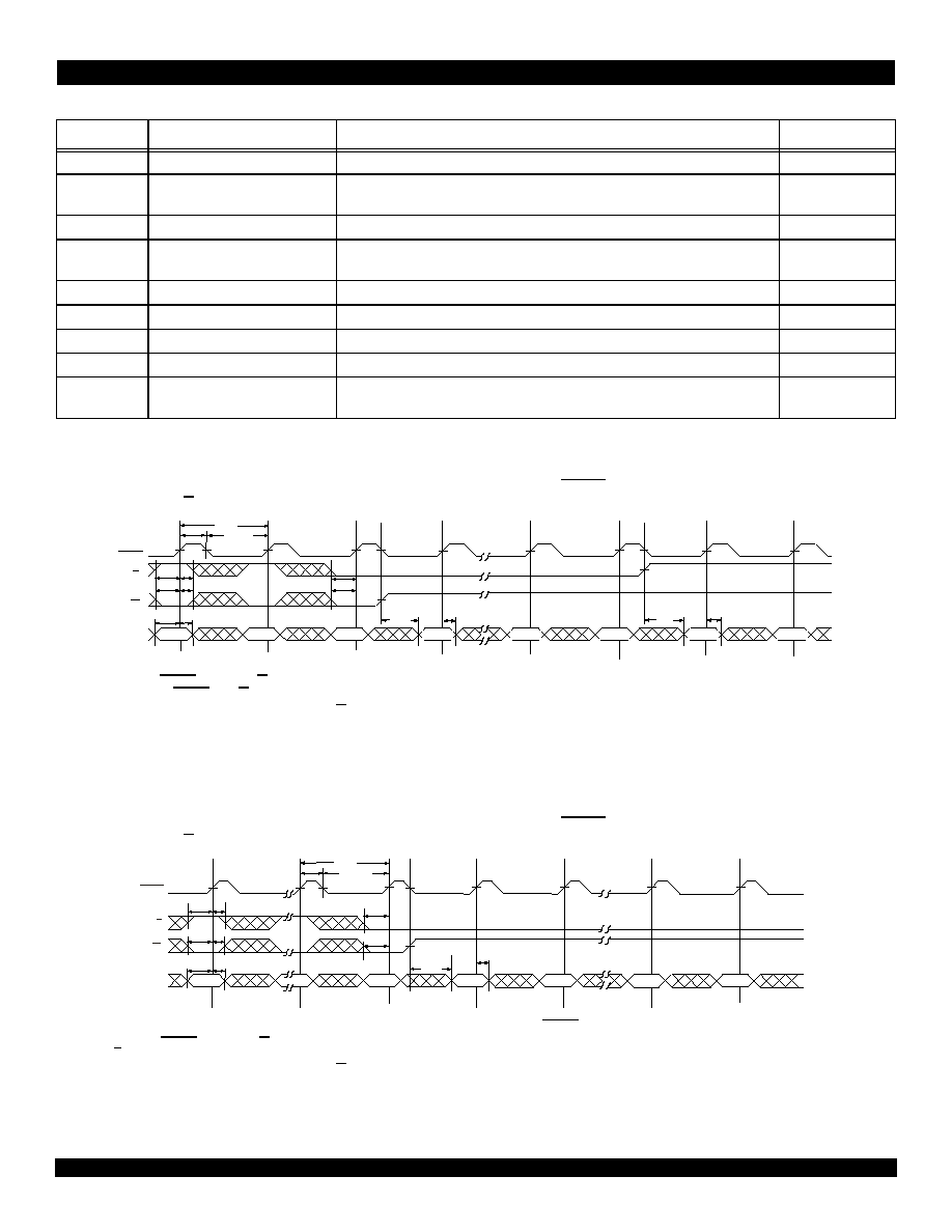
Reset Waveforms
Reset Waveforms
Reset Waveforms
Reset Waveforms
1
RESETI must be held HIGH for 8 SCLK cycles. When RESETI goes Low again 8191 cycles are used prior to the Status Acknowledge bits showing the internal reset process is com-
plete.
2
This delay should typically be much less than two SCLK cycles. RESETO remains High until START Command is received from the Call Setup Manager.
1
2
SCLK
CBRCLKx
100
200
300
400
3
100
200
300
400
1
2
3607 drw 12
100
SCLK
2
cont'd
waveform
CBRCLKx
1
see cont'd
waveform
3607 drw 13
3
200
300
100
400
SCLK
RESETI
3607 drw 14
1
2
7
8
1
2
8190
8191
1
t
RSI
RESETO
1
2
2
2 clock cycles max.

13 of 17
April 11, 2001
IDT77V500
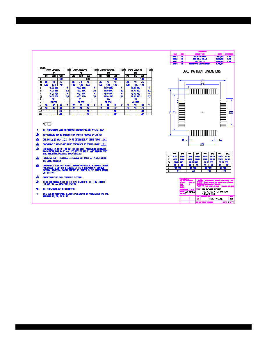
77V500 Package Drawing -- 100-pin TQFP
77V500 Package Drawing -- 100-pin TQFP
77V500 Package Drawing -- 100-pin TQFP
77V500 Package Drawing -- 100-pin TQFP
14 of 17
April 11, 2001
IDT77V500
77V500 Package Drawing -- 100-pin TQFP (Page Two)
77V500 Package Drawing -- 100-pin TQFP (Page Two)
77V500 Package Drawing -- 100-pin TQFP (Page Two)
77V500 Package Drawing -- 100-pin TQFP (Page Two)
15 of 17
April 11, 2001
IDT77V500
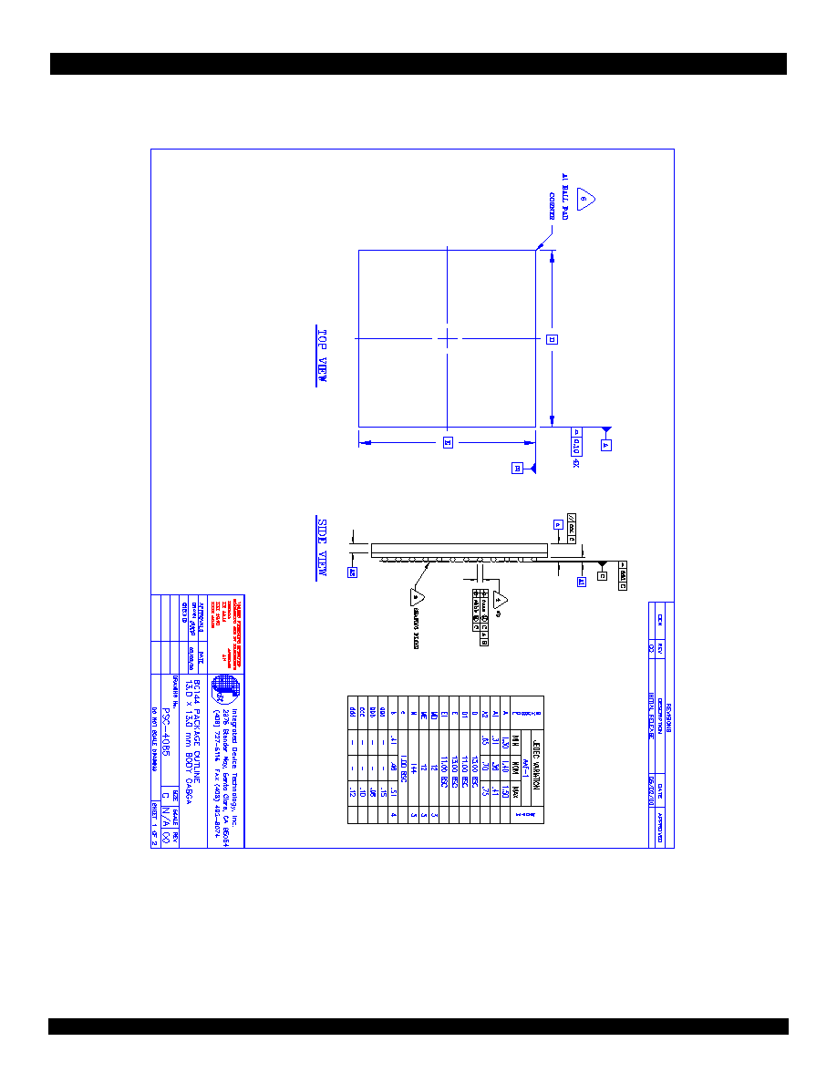
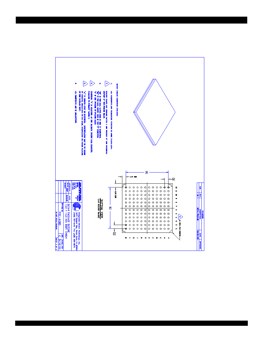
77V500 Package Drawing -- 144-ball BGA
77V500 Package Drawing -- 144-ball BGA
77V500 Package Drawing -- 144-ball BGA
77V500 Package Drawing -- 144-ball BGA
16 of 17
April 11, 2001
IDT77V500
77V500 Package Drawing
77V500 Package Drawing
77V500 Package Drawing
77V500 Package Drawing
--
--
--
--
144-ball (Page Two)
144-ball (Page Two)
144-ball (Page Two)
144-ball (Page Two)
17 of 17
April 11, 2001
IDT77V500
CORPORATE HEADQUARTERS
2975 Stender Way
Santa Clara, CA 95054
for SALES:
800-345-7015
or 408-727-6116
fax:
408-330-1748
www.idt.com
for Tech Support:
switchstarhelp@idt.com
phone:
408-492-8208
SwitchStar and the IDT logo are registered trademarks of Integrated Device Technology, Inc.
Datasheet Document History
Datasheet Document History
Datasheet Document History
Datasheet Document History
Ordering Information
Ordering Information
Ordering Information
Ordering Information
3/1/99:
Updated to new format.
Added Industrial Specifications.
Added S25 Speed Grade.
Pg. 3
Package Diagram notes added for clarification.
Pg. 4
Pin description table descriptions corrected. OFRM and Vss pin number corrections made.
Pg. 5
V
TERM
in Maximum ratings table reduced to 3.9V.
Pg. 10
Manager Bus Sequence Waveforms on page 9 and page 10 and their notes modified for clarity.
Pg. 14
Updated Ordering Information for S156 speed grade and Industrial temperature product. Added Preliminary Datasheet definition and
Datasheet Document History.
12/11/00:
Moved to final.
Updated general format and SwitchStar logo.
Pg. 6
Corrected t
DCC
,
t
DCS
,
t
DCIO
,
t
OHMD
,
and
t
DCOF
test limits to minimum values instead of maximum values.
Pg. 8
Clarified OFRM signal on SFRM, CBUS, and OFRM timing waveforms.
Pg. 10
Clarified CBR delays in text.
Pg. 11
Clarified SCLK timing in CBR Clock Functional Waveform Example 1 and added information to footnote 1.
Pg. 12
Corrected package designator to PN100-1. Updated Tech Support phone number.
1/30/01:
Added BGA package to pages 1, 2, 3, 4,5, and 12.
4/11/01:
Deleted S27 speed grade on pages 8 and 15. Added 100-pin TQFP and 144-ball BGA package drawings.
A
Power
99
Speed
A
Package
A
Process/
Temperature
Range
Blank
I
Commercial (0
∞
C to +70
∞
C)
Industrial (-40
∞
C to +85
∞
C)
PF
BC
100-pin TQFP (PN100-1)
144-Ball BGA (BC144-1)
25
S
Standard Power
XXXXX
Device
Type
ATM Cell Based Switch Controller
77V500
IDT
3607 drw sp15
System Clock Period in ns
Commercial & Industrial
,