©1999 Integrated Device Technology, Inc.
6.06
MARCH 1999
DSC 3607/3
1
PRELIMINARY
IDT77V500
Features
x
Single chip controller for IDT77V400 Switching Memory
x
One IDT77V500 and one IDT77V400 form the core required
for a 1.24Gbps 8 x 8 port non-blocking switch
x
Supports up to 8192 Virtual Connections (VCs)
x
Per VC queuing for fairness, with four priorities per VC
available for each output port of the switch
x
Capable of supporting CBR, VBR, UBR, and ABR (EFCI)
service classes
x
Low power dissipation
≠430mW (typ.)
x
Optional header modification operation
x
Multicasting and Broadcasting capability
x
Provides congestion management support through EFCI,
CLP, and EPD functionality
x
System clock cycle times as fast as 27ns (37MHz)
x
Option available for resolving contention issues between
multiple IDT77V500 configurations
SWITCHStAR
TM
ATM CELL BASED
1.24Gbps NON-BLOCKING
INTEGRATED SWITCH CONTROLLER
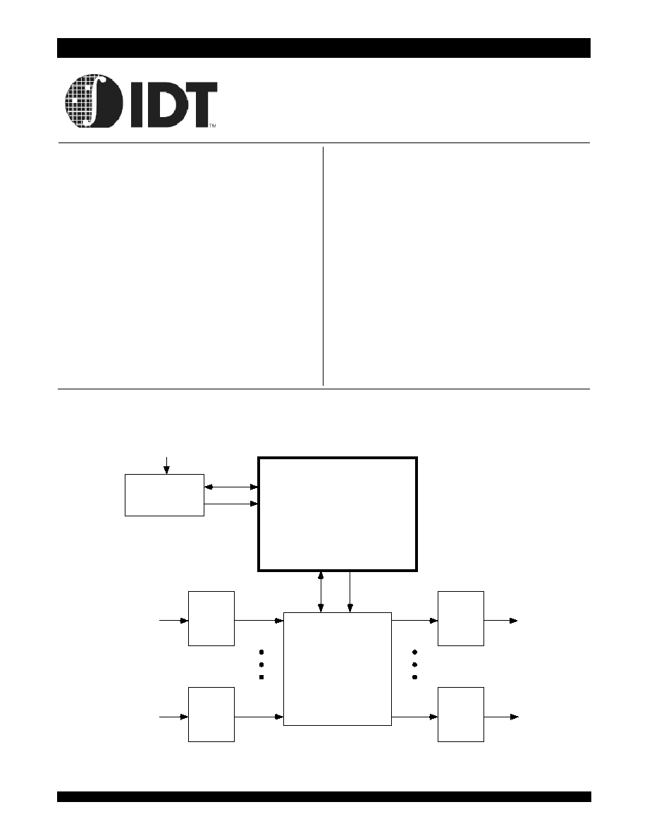
Typical 8 x 8 Switch Configuration using the IDT77V500 Switch Controller
x
One IDT77V500 can manage up to eight IDT77V400's
without derating for larger switch configurations
x
Industrial temperature range (-40∞ C to +85∞ C) is available
x
Single +3.3V ± 300mV power supply
x
Available in a 100-pin Thin Plastic Quad Flat Pack (TQFP)
Description
The IDT77V500 ATM Cell Based Switch Controller, when paired
with the IDT77V400 Switching Memory, forms the core control logic
and switch fabric for a 1.24Gbps non-blocking ATM switch. The
IDT77V500 manages all of the switch traffic moving through the
IDT77V400, commanding the storage of incoming ATM cells and
interpreting and modifying the cell header information as necessary
for data flow through the switch. It then uses the header information,
including priority indicators, to queue and direct the individual cells for
transmission out the appropriate output port of the IDT77V400.
The IDT77V500 utilizes Per Virtual Connection (VC) Queuing to
keep track of each call, and has the capacity to keep track of as many
8-bit Processor/
Call Setup
Manager
IDT77V500
Switch
Controller
IDT77V400
Switching
Memory
IDT77155
155Mbps
PHY
Port 0
Port 0
Port 7
Port 7
Control
Control
Data
Data
External Interface
for Global Setup
and Control
3607 drw 01
(for example,
IDT77V550
IDT79RV3041,
IDT79R36100,
or IDT79RV4640)
IDT77155
155Mbps
PHY
IDT77155
155Mbps
PHY
IDT77155
155Mbps
PHY
/

6.42
IDT77V500 Preliminary
SWITCHStAR Switch Controller Industrial and Commercial Temperature Range
2
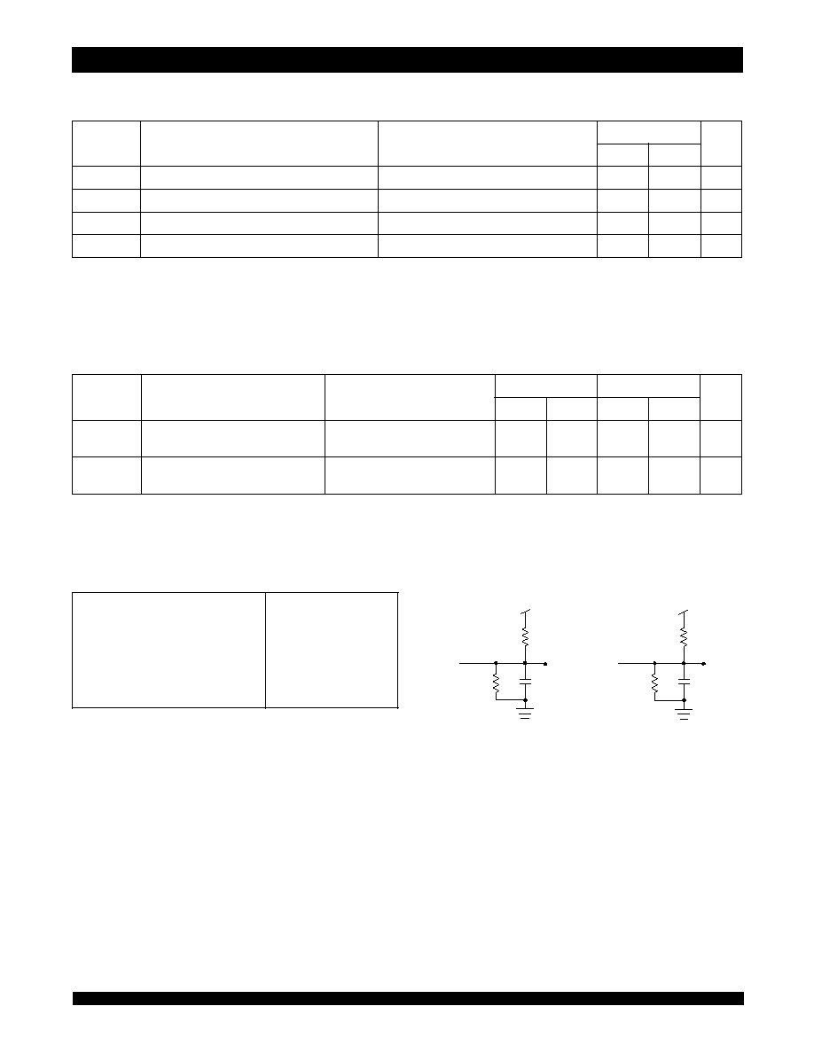
Functional Block Diagram
NOTES:
1. SCLK and Reset are inputs to all blocks.
2. Outputs are always enabled (active).
Description (cont.)
as 8192 individual VC queues. There are four possible priorities
available for each of the assigned outputs of the Switching Memory,
and CBR, VBR, UBR, and ABR-EFCI service classes are supported
by the Switch Controller. Multicasting and broadcasting services are
provided, requiring only the appropriate header information to execute
these operations automatically without requiring multiple Switching
Memory entries.
The IDT77V500 also has a mode for managing and transmitting
pocketized data, enabling easy transition between packet oriented
networks such as Ethernet and FDDI and ATM cell oriented networks.
The IDT77V500 has an 8-bit Manager Bus interface, MDATA0-7, to
a Call Setup Manager processor for the configuration activity and call
setup operation. When a Call Setup Cell is received by the IDT77V400,
the cell is directed to a specified output port and the payload
processed by the Call Setup Manager. The new Virtual Connection
(VC) is then established in the Queue Manager of the IDT77V500,
with all operations executed across the 8-bit Manager Bus. Subse-
quent cells of that particular VC are then prioritized and directed by the
Switch Controller as they are received by the IDT77V400; no further
interaction with the Call Manager processor is required for ongoing
queue and cell management.
The IDT77V500 supports a major subset of the available com-
mands and configurations of the IDT77V400 Switching Memory.
Please refer to the SWITCHStAR User Manual for additional feature
details and implementation information.
The IDT77V500 is fully 3.3V LVTTL compatible, and is packaged
in an 100-pin Thin Plastic Quad Flatpack (TQFP).
IOD0-31
32
Control
Logic
OFRM0-7
CRCERR
SCLK
CMD0-5
6
3607 drw 02
Call
Setup
Manager
MDATA0-7
MSTRB
MD/
C
MR/
W
Switching Memory Interface
Output
Service
and
Arbitration
State
Machine
Queue Manager
Output Queues
and
Link Registers
RESETI
RESETO
CBRCLK2
CBRCLK3
SFRM
Reset
(1)
SCLK
(1)
(2)
(2)
(2)

6.42
IDT77V500 Preliminary
SWITCHStAR Switch Controller Industrial and Commercial Temperature Range
3
Package Diagram
(1,2,3)
100 99 98 97 96 95 94 93 92 91 90 89 88 87 86 85 84 83 82 81 80 79 78 77 76
IOD
5
IOD
4
V
SS
V
CC
IOD
3
IOD
2
IOD
1
CRCERR
V
CC
MDATA
0
MDATA
1
MDATA
2
V
CC
V
SS
MDATA
5
MDATA
6
MDATA
3
MDATA
4
NC
NC
NC
Index
1
2
3
4
5
6
7
8
9
10
11
12
13
14
15
16
17
18
19
20
21
22
23
24
25
NC
NC
RESETI
NC
NC
NC
CMD3
MSTRB
MR/
W
NC
CMD4
CMD5
V
CC
IOD
24
NC
NC
75
74
73
72
71
70
69
68
67
66
65
64
63
62
61
60
59
58
57
56
55
54
53
52
51
NC
IOD
13
V
CC
V
SS
IOD
11
IOD
10
IOD
9
IOD
8
IOD
7
NC
NC
IOD
12
26 27 28 29 30 31 32 33 34 35 36 37 38 39 40 41 42 43 44 45 46 47 48 49 50
IDT77V500PF
PN100-1
(4)
100-Pin TQFP
Top View
(5)
3607 drw 03
V
CC
V
CC
IOD
0
IOD
6
IOD
14
IOD
15
IOD
16
IOD
17
IOD
18
IOD
19
NC
V
SS
V
CC
IOD
20
IOD
21
IOD
22
IOD
23
NC
V
SS
IOD
25
IOD
26
IOD
27
IOD
28
IOD
29
IOD
30
IOD
31
V
SS
V
SS
V
SS
V
CC
V
SS
OFRM
0
OFRM
1
OFRM
2
OFRM
3
OFRM
4
OFRM
5
OFRM
6
MDATA
7
MD/
C
V
CC
V
SS
CMD2
CMD1
CMD0
RESETO
SCLK
CBRCLK2
CBRCLK3
SFRM
OFRM7
NOTES:
1. All V
CC
pins must be connected to power supply.
2. All V
SS
pins must be connected to ground supply.
3. Package body is approximately 14mm x 14mm x 1.4mm.
4. This package code is used to reference the package diagram.
5. This text does not indicate orientation of the actual part marking.

6.42
IDT77V500 Preliminary
SWITCHStAR Switch Controller Industrial and Commercial Temperature Range
4
Pin Description
r
e
b
m
u
N
n
i
P
l
o
b
m
y
S
e
p
y
T
n
o
it
p
ir
c
s
e
D
8
1
K
L
C
S
I
ll
A
.r
e
ll
o
rt
n
o
C
h
ct
i
w
S
0
0
5
V
7
7
T
D
I
e
h
t
f
o
s
n
i
p
s
u
o
n
o
r
h
c
n
y
s
ll
a
r
o
f
t
u
p
n
i
k
c
o
lc
e
c
n
e
r
e
r
e
f
e
R
:
k
c
o
lc
m
e
t
s
y
S
.
K
L
C
S
f
o
e
g
d
e
g
n
is
ir
e
h
t
o
t
d
e
c
n
e
r
e
f
e
r
e
r
a
sl
a
n
g
is
s
u
o
n
o
r
h
c
n
y
s
0
2
,
2
2
,
3
K
L
C
R
B
C
2
K
L
C
R
B
C
I
.
d
e
zi
lit
u
e
r
a
s
e
s
s
a
lc
e
ci
v
r
e
S
)
R
B
C
(
e
t
a
R
ti
B
t
n
a
t
s
n
o
C
n
e
h
w
d
e
s
u
sl
a
n
g
is
k
c
o
lc
la
n
r
e
t
x
E
:
2
d
n
a
3
s
k
c
o
l
C
R
B
C
e
h
t
e
n
i
m
r
e
t
e
d
o
t
d
e
s
u
e
r
a
d
n
a
yl
e
vi
t
c
e
p
s
e
r
2
d
n
a
3
s
e
iti
r
o
ir
p
tr
o
P
t
u
p
t
u
O
o
t
d
n
o
p
s
e
rr
o
c
sl
a
n
g
is
k
c
o
lc
e
s
e
h
T
d
lu
o
h
s
s
n
i
p
e
s
e
h
t
d
e
s
u
t
o
n
si
e
d
o
m
R
B
C
fI
.y
ti
r
o
ir
p
t
s
e
h
g
ih
e
h
t
si
3
yt
ir
o
ir
P
.r
e
ll
o
rt
n
o
c
e
h
t
r
o
f
e
t
a
r
ti
b
t
n
a
t
s
n
o
c
.
s
s
e
l
r
o
m
h
o
K
5
f
o
e
u
la
v
d
e
d
n
e
m
m
o
c
e
r
a
h
ti
w
r
o
t
si
s
e
r
a
h
ti
w
c
c
V
o
t
p
u
d
e
ll
u
p
e
b
6
8
R
R
E
C
R
C
I
.
K
L
C
S
f
o
e
g
d
e
g
n
is
ir
e
h
t
n
o
t
u
p
n
i
s
u
o
n
o
r
h
c
n
y
S
:r
o
rr
E
k
c
e
h
C
y
c
n
a
d
n
u
d
e
R
la
ci
lc
y
C
R
R
E
C
R
C
y
b
W
O
L
d
e
tr
e
s
s
a
e
h
t
n
i
d
e
r
u
c
c
o
s
a
h
r
o
rr
e
C
R
C
C
E
H
a
t
a
h
t
s
e
t
a
ci
d
n
i
n
o
it
a
r
e
p
o
e
r
o
t
s
a
g
n
ir
u
d
y
r
o
m
e
M
g
n
ih
ct
i
w
S
0
0
4
V
7
7
T
D
I
e
h
t
.r
e
d
a
e
h
ll
e
c
2
/
D
M C
I
/
D
M
.
n
o
it
a
r
e
p
O
s
u
B
r
e
g
a
n
a
M
e
h
t
r
o
f
0
0
5
V
7
7
T
D
I
e
h
t
f
o
s
r
e
t
si
g
e
r
l
o
rt
n
o
c
r
o
a
t
a
d
e
h
t
st
c
e
l
e
S
:l
o
rt
n
o
C
r
e
g
a
n
a
M
C
/
D
M
d
n
a
,
s
r
e
t
si
g
e
r
a
t
a
d
e
h
t
st
c
e
l
e
s
H
G
I
H
d
e
tr
e
s
s
a
C
e
h
t
f
o
s
r
e
t
si
g
e
r
s
u
t
a
t
s
/
d
n
a
m
m
o
c
e
h
t
st
c
e
l
e
s
W
O
L
.
0
0
5
V
7
7
T
D
I
3
/
R
M W
I
/
R
M
:
e
ti
r
W
/
d
a
e
R
r
e
g
a
n
a
M
W
e
h
t
y
b
d
e
t
c
e
l
e
s
s
r
e
t
si
g
e
r
e
h
t
o
t
n
i
s
u
B
r
e
g
a
n
a
M
e
h
t
n
o
a
t
a
d
e
h
t
e
ti
r
w
lli
w
W
O
L
/
D
M C
/
R
M
(
e
d
o
m
e
ti
r
w
n
I
.t
u
p
n
i
W
e
h
t
o
t
t
c
e
p
s
e
r
h
ti
w
yl
s
u
o
n
o
r
h
c
n
y
s
n
e
tti
r
w
si
7
-
0
A
T
A
D
M
n
o
a
t
a
d
e
h
t
)
W
O
L
f
o
e
g
d
e
g
n
is
ir
B
R
T
S
M
/
R
M
(
e
d
o
m
d
a
e
r
n
i
;
W
.y
ls
u
o
n
o
r
h
c
n
y
s
a
d
e
s
s
e
c
c
a
si
a
t
a
d
e
h
t
)
H
G
I
H
4
B
R
T
S
M
I
e
r
a
st
u
p
n
i
s
u
B
r
e
g
a
n
a
M
r
e
h
t
O
.)
7
-
0
A
T
A
D
M
(
s
u
B
r
e
g
a
n
a
M
e
h
t
r
o
f
k
c
o
lc
a
s
a
st
c
a
h
ci
h
w
t
u
p
n
I
:
e
b
o
rt
S
r
e
g
a
n
a
M
f
o
e
g
d
e
g
n
is
ir
e
h
t
o
t
s
u
o
n
o
r
h
c
n
y
s
B
R
T
S
M
/
R
M
(
s
n
o
it
a
r
e
p
o
e
ti
r
w
g
n
ir
u
d
W
d
e
ifi
c
e
p
s
e
h
t
t
e
e
m
t
s
u
m
d
n
a
)
W
O
L
.
s
r
e
t
e
m
a
r
a
p
d
l
o
H
d
n
a
p
u
t
e
S
B
R
T
S
M
n
o
it
a
r
e
p
o
d
a
e
r
a
n
e
h
w
n
o
it
c
n
u
f
e
l
b
a
n
E
t
u
p
t
u
O
s
u
o
n
o
r
h
c
n
y
s
a
n
a
s
m
r
o
fr
e
p
/
R
M
(
W
n
e
h
W
.
s
u
B
r
e
g
a
n
a
M
e
h
t
n
o
d
e
t
u
c
e
x
e
si
)
H
G
I
H
B
R
T
S
M
/
R
M
d
n
a
W
O
L
si
W
e
h
t
)
e
d
o
M
d
a
e
R
(
H
G
I
H
si
/
D
M
e
h
t
y
b
d
e
n
i
m
r
e
t
e
d
(
s
r
e
t
si
g
e
r
0
0
5
V
7
7
T
D
I
e
h
t
f
o
st
n
e
t
n
o
c
e
h
t
d
n
a
e
d
o
m
t
u
p
t
u
o
n
i
d
e
l
b
a
n
e
si
s
u
B
r
e
g
a
n
a
M
C
.
7
-
0
A
T
A
D
M
n
o
d
a
e
r
e
b
o
t
e
l
b
a
li
a
v
a
e
r
a
)t
u
p
n
i
7
1
I
T
E
S
E
R
I
e
h
t
f
o
e
c
n
e
u
q
e
s
t
e
s
e
r
la
n
r
e
t
n
i
e
h
t
s
e
t
a
iti
n
i
yl
s
u
o
n
o
r
h
c
n
y
s
a
la
n
g
is
si
h
t
,
H
G
I
H
d
e
tr
e
s
s
a
n
e
h
W
:t
u
p
n
I
t
e
s
e
R
.
0
0
5
V
7
7
T
D
I
9
1
O
T
E
S
E
R
O
0
0
5
V
7
7
T
D
I
e
l
p
itl
u
m
n
I
.)
H
G
I
H
I
T
E
S
E
R
(
0
0
5
V
7
7
T
D
I
e
h
t
f
o
t
e
s
e
r
e
h
t
g
n
it
a
iti
n
i
n
o
p
u
H
G
I
H
d
e
tr
e
s
s
A
:t
u
p
t
u
O
t
e
s
e
R
lli
w
O
T
E
S
E
R
.
n
ia
h
c
e
h
t
n
i
r
e
ll
o
rt
n
o
c
t
x
e
n
e
h
t
f
o
t
u
p
n
i
I
T
E
S
E
R
e
h
t
o
t
d
e
t
c
e
n
n
o
c
si
t
u
p
t
u
o
si
h
t
,
s
n
o
it
a
r
u
g
if
n
o
c
.r
e
g
a
n
a
M
p
u
t
e
S
ll
a
C
e
h
t
m
o
rf
d
e
vi
e
c
e
r
si
d
n
a
m
m
o
c
T
R
A
T
S
a
lit
n
u
H
G
I
H
n
ia
m
e
r
4
1
-
2
1
,
9
-
7
5
-
0
D
M
C
O
e
r
a
y
r
o
m
e
m
g
n
ih
ct
i
w
S
0
0
4
V
7
7
T
D
I
e
h
t
y
b
d
e
t
u
c
e
x
e
e
b
o
t
s
n
o
it
c
u
rt
s
n
i
,
K
L
C
S
h
ti
w
d
e
zi
n
o
r
h
c
n
y
S
:
s
u
B
d
n
a
m
m
o
C
.
s
u
b
ti
b
-
6
si
h
t
n
o
0
0
5
V
7
7
T
D
I
e
h
t
y
b
t
u
p
t
u
o
4
2
M
R
F
S
O
.
s
u
b
n
o
m
m
o
c
a
r
o
f
d
n
e
t
n
o
c
s'
0
0
5
V
7
7
T
D
I
e
l
p
itl
u
m
n
e
h
w
d
e
s
u
t
u
p
t
u
o
s
u
o
n
o
r
h
c
n
y
S
:
e
m
a
r
F
t
u
p
t
u
O
e
zi
n
o
r
h
c
n
y
S
.
s
0
0
5
V
7
7
T
D
I
r
e
h
t
o
e
h
t
f
o
t
u
p
n
i
0
M
R
F
O
e
h
t
s
e
vi
r
d
n
e
h
t
h
ci
h
w
la
n
g
is
si
h
t
s
e
t
a
r
e
n
e
g
0
0
5
V
7
7
T
D
I
r
e
t
s
a
M
e
h
T
,
9
4
-
6
4
,
3
4
-
0
4
,
6
6
-
9
5
,
6
5
-
3
5
9
7
-
7
7
,
3
7
-
9
6
5
8
-
2
8
1
3
-
0
D
O
I
O
/I
r
o
f
d
e
s
U
.)
5
-
0
D
M
C
(
s
u
B
d
n
a
m
m
o
C
e
h
t
o
t
t
n
e
t
a
l
e
lc
y
c
e
n
o
d
n
a
K
L
C
S
h
ti
w
s
u
o
n
o
r
h
c
n
y
S
:
s
u
B
a
t
a
D
l
o
rt
n
o
C
s
s
e
r
d
d
a
y
r
o
m
e
m
ll
e
c
e
h
t
d
n
a
,
s
r
e
t
si
g
e
r
s
u
t
a
t
s
d
n
a
r
o
rr
e
,r
e
t
si
g
e
r
n
o
it
a
r
u
g
if
n
o
c
,
s
e
t
y
b
r
e
d
a
e
h
e
h
t
f
o
r
e
f
s
n
a
rt
.y
r
o
m
e
M
g
n
ih
ct
i
w
S
0
0
4
V
7
7
T
D
I
e
h
t
d
n
a
0
0
5
V
7
7
T
D
I
e
h
t
n
e
e
w
t
e
b
8
9
-
6
9
,
3
9
-
0
9
,
1
7
-
6
A
T
A
D
M
O
/I
-i
b
ti
b
-
8
si
h
t
r
e
v
o
r
u
c
c
o
0
0
5
V
7
7
T
D
I
e
h
t
d
n
a
r
e
g
a
n
a
M
p
u
t
e
S
ll
a
C
e
h
t
n
e
e
w
t
e
b
s
n
o
it
a
ci
n
u
m
m
o
C
:
s
u
B
r
e
g
a
n
a
M
/
D
M
.
s
u
b
la
n
o
it
c
e
ri
d
C
/
R
M
,
W
d
n
a
,
B
R
T
S
M
A
T
A
D
M
e
h
t
s
s
o
r
c
a
d
e
rr
e
f
s
n
a
rt
e
p
yt
a
t
a
d
d
n
a
e
d
o
m
e
h
t
e
n
i
m
r
e
t
d
o
t
t
c
e
p
s
e
r
h
ti
w
s
u
o
n
o
r
h
c
n
y
s
e
r
a
s
n
o
it
a
r
e
p
o
e
ti
r
W
.
s
u
b
B
R
T
S
M
d
a
e
r
r
o
f
yl
s
u
o
n
o
r
h
c
n
y
s
a
s
e
v
a
h
e
b
A
T
A
D
M
e
li
h
w
,
.
s
n
o
it
a
r
e
p
o
,
9
2
-
8
2
,
5
2
6
3
,
5
3
-
2
3
7
-
1
M
R
F
O
0
M
R
F
O
O
/I
I
o
t
d
e
d
a
o
l
e
b
n
a
c
ll
e
c
t
x
e
n
e
h
t
n
e
h
w
t
c
e
t
e
d
o
t
0
0
5
V
7
7
T
D
I
e
h
t
y
b
d
e
s
u
s
n
i
p
t
u
p
n
i
s
u
o
n
o
r
h
c
n
y
s
A
:
e
m
a
r
F
t
u
p
t
u
O
e
r
a
7
-
1
M
R
F
O
e
h
t
,
s
n
o
it
a
r
u
g
if
n
o
c
0
0
5
V
7
7
T
D
I
e
l
p
itl
u
m
n
i
n
e
h
W
.
7
h
g
u
o
r
h
t
0
tr
o
p
t
u
p
t
u
o
0
0
4
V
7
7
T
D
I
d
e
ifi
c
e
p
s
e
h
t
.)
0
S
U
B
C
o
n
si
e
r
e
h
T
(
n
i
p
t
u
p
n
i
n
a
s
y
a
w
la
si
0
M
R
F
O
.
n
o
it
a
rt
i
b
r
a
r
o
f
7
-
1
S
U
B
C
s
a
d
e
n
if
e
d
e
r
,
8
5
,
5
4
,
1
3
,
1
1
4
9
,
9
8
-
7
8
,
1
8
,
8
6
V
C
C
r
e
w
o
P
V
3
.
3
+
(
yl
p
p
u
S
r
e
w
o
P
+
)
V
m
0
0
3
,
9
3
-
7
3
,
0
3
,
0
1
,
0
8
,
7
6
,
7
5
,
4
4
5
9
V
S
S
r
e
w
o
P
d
n
u
o
r
G
,
3
2
,
1
2
,
6
1
-
5
1
,
6
-
5
,
7
2
-
6
2
,
6
7
-
4
7
,
2
5
-
0
5
0
0
1
-
9
9
C
N
_
_
_
_
t
c
e
n
n
o
C
o
N
1
0
l
b
t
7
0
6
3

6.42
IDT77V500 Preliminary
SWITCHStAR Switch Controller Industrial and Commercial Temperature Range
5
Absolute Maximum Ratings
(1)
NOTES:
1.
Stresses greater than those listed under ABSOLUTE MAXIMUM RATINGS may
cause permanent damage to the device. This is a stress rating only and functional
operation of the device at these or any other conditions above those indicated in the
operational sections of this specification is not implied. Exposure to absolute
maximum rating conditions for extended periods may affect reliability.
2.
V
TERM
must not exceed Vcc + 0.3V for more than 25% of the cycle time or 10ns
maximum, and is limited to < 20mA for the period of V
TERM
> Vcc + 0.3V.
Recommended DC Operating
Conditions
(2)
NOTES:
1. These parameters are determined by device characterization, but are not
production tested.
2. 3dV references the interpolated capacitance when the input and output switch from
0V to 3V or from 3V to 0V.
3. C
OUT
also references C
I/O
.
Capacitance
(T
A
= +25∞C, f = 1.0MH
z
)
TQFP ONLY
NOTES:
1.
V
IL
> -1.5V for pulse width less than 10ns.
2.
V
TERM
must not exceed Vcc + 0.3V or Vss ≠ 0.3V.
3.
V
TERM
must not exceed Vcc + 0.3V for more than 25% of the cycle time or 10ns
maximum, and is limited to < 20mA for the period of V
TERM
> Vcc + 0.3V.
Maximum Operating
Temperature and Supply Voltage
(1)
l
o
b
m
y
S
g
n
it
a
R
l
a
i
c
r
e
m
m
o
C
l
a
ir
t
s
u
d
n
I
&
ti
n
U
V
M
R
E
T
)
2
(
e
g
a
tl
o
V
la
n
i
m
r
e
T
t
c
e
p
s
e
R
h
ti
w
D
N
G
o
t
9
.
3
+
o
t
5
.
0
-
V
T
S
A
I
B
e
r
u
t
a
r
e
p
m
e
T
s
a
i
B
r
e
d
n
U
5
2
1
+
o
t
5
5
-
o
C
T
G
T
S
e
g
a
r
o
t
S
e
r
u
t
a
r
e
p
m
e
T
5
2
1
+
o
t
5
5
-
o
C
I
T
U
O
t
u
p
t
u
O
C
D
t
n
e
rr
u
C
0
5
A
m
2
0
l
b
t
7
0
6
3
e
d
a
r
G
t
n
e
i
b
m
A
e
r
u
t
a
r
e
p
m
e
T
D
N
G
c
c
V
la
ic
r
e
m
m
o
C
0
O
0
7
+
o
t
C
O
C
V
0
V
3
.
3
+
V
3
.
0
la
irt
s
u
d
n
I
0
4
-
O
5
8
+
o
t
C
O
C
V
0
V
3
.
3
+
V
3
.
0
3
0
l
b
t
7
0
6
3
l
o
b
m
y
S
r
e
t
e
m
a
r
a
P
.
n
i
M
.
p
y
T
.x
a
M
ti
n
U
V
C
C
e
g
a
tl
o
V
yl
p
p
u
S
0
.
3
3
.
3
6
.
3
V
V
S
S
d
n
u
o
r
G
0
0
0
V
V
H
I
t
u
p
n
I
e
g
a
tl
o
V
h
g
i
H
0
.
2
_
_
_
_
V
C
C
V
3
.
0
+
)
3
(
V
V
L
I
w
o
L
t
u
p
n
I
e
g
a
tl
o
V
5
.
0
-
)
1
(
_
_
_
_
8
.
0
V
4
0
l
b
t
7
0
6
3
l
o
b
m
y
S
r
e
t
e
m
a
r
a
P
s
n
o
i
t
i
d
n
o
C
)
2
(
.
x
a
M
t
i
n
U
C
N
I
e
c
n
a
ti
c
a
p
a
C
t
u
p
n
I
V
N
I
V
d
3
=
9
F
p
C
T
U
O
)
3
(
e
c
n
a
ti
c
a
p
a
C
t
u
p
t
u
O
V
T
U
O
V
d
3
=
0
1
F
p
5
0
l
b
t
7
0
6
3
NOTE:
1. This is the parameter T
A
.
6.42
IDT77V500 Preliminary
SWITCHStAR Switch Controller Industrial and Commercial Temperature Range
6
NOTE:
1. At f = f
max
SCLK is cycling at maximum frequency and all inputs are cycling at 1/t
CYC1
, using AC input levels of V
SS
to 3.0V.
DC Electrical Ccharacteristics Over the Operating
Temperature and Supply Voltage Range
(V
CC
= 3.3V ± 0.3V)
DC Electrical Characteristics Over the Operating
Temperature and Supply Voltage Range
(V
CC
= 3.3V ± 0.3V)
AC Test Conditions
NOTE:
1. For MDATA, IOD, and OFRM pins only.
Figure 1. AC Output Test Load
l
o
b
m
y
S
r
e
t
e
m
a
r
a
P
s
n
o
it
i
d
n
o
C
t
s
e
T
S
0
0
5
V
7
7
ti
n
U
.
n
i
M
.x
a
M
I|
LI
|
t
n
e
rr
u
C
e
g
a
k
a
e
L
t
u
p
n
I
V
C
C
V
,
V
6
.
3
=
N
I
V
o
t
V
0
=
C
C
_
_
_
0
1
A
µ
I|
O
L
|
)
1
(
t
n
e
rr
u
C
e
g
a
k
a
e
L
t
u
p
t
u
O
V
=
I
T
S
E
R
H
I
V
,
T
U
O
V
o
t
V
0
=
C
C
_
_
_
0
1
A
µ
V
L
O
e
g
a
tl
o
V
w
o
L
t
u
p
t
u
O
I
L
O
A
m
4
+
=
_
_
_
4
.
0
V
V
H
O
e
g
a
tl
o
V
h
g
i
H
t
u
p
t
u
O
I
H
O
A
m
4
-
=
4
.
2
_
_
_
V
6
0
l
b
t
7
0
6
3
I
F
P
7
2
/
5
2
S
0
0
5
V
7
7
F
P
7
2
/
5
2
S
0
0
5
V
7
7
l
o
b
m
y
S
r
e
t
e
m
a
r
a
P
n
o
it
i
d
n
o
C
t
s
e
T
.
p
y
T
.x
a
M
.
p
y
T
.x
a
M
ti
n
U
I
C
C
t
n
e
rr
u
C
g
n
it
a
r
e
p
O
V
C
C
V
=
I
T
E
S
E
R
,
V
6
.
3
=
L
I
,
f
=
f
X
A
M
)
1
(
0
3
1
0
0
2
0
3
1
5
7
1
A
m
I
R
C
C
t
n
e
rr
u
C
t
e
s
e
R
V
C
C
V
=
I
T
E
S
E
R
,
V
6
.
3
=
H
I
,
f
=
f
X
A
M
)
1
(
0
5
1
5
2
3
0
5
1
0
0
3
A
m
7
0
l
b
t
7
0
6
3
s
l
e
v
e
L
e
s
l
u
P
t
u
p
n
I
s
e
m
i
T
ll
a
F
/
e
s
i
R
t
u
p
n
I
s
l
e
v
e
L
e
c
n
e
r
e
f
e
R
g
n
i
m
i
T
t
u
p
n
I
s
l
e
v
e
L
e
c
n
e
r
e
f
e
R
t
u
p
t
u
O
d
a
o
L
t
u
p
t
u
O
V
S
S
V
0
.
3
o
t
.
x
a
M
s
n
3
V
5
.
1
V
5
.
1
2
d
n
a
1
s
e
r
u
g
i
F
8
0
l
b
t
7
0
6
3
Figure 2. Output Test Load
(for High-Impedance parameters)
* Including scope and jig.
3607 drw 05
590
50pF
435
3.3V
DATA
OUT
590
5pF*
435
3.3V
DATA
OUT
3607 drw 04

6.42
IDT77V500 Preliminary
SWITCHStAR Switch Controller Industrial and Commercial Temperature Range
7
NOTES:
1. RESETI must be held High for 8 SCLK cycles. After RESETI transitions Low 8191 cycles are required before the Status Acknowledge bits will indicate that the internal
reset process in complete.
2. Transition is measured +/-200mV from Low or High impedance voltage with the Output Test Load (Figure 2).
This parameter is guaranteed by device characterization, but is not production tested.
3. Cycle units insure that the SCLK recognizes the state of CBRCLK.
AC Electrical Characteristics Over the Operating Temperature Range
(V
CC
= 3.3V ± 0.3V)
5
2
S
0
0
5
V
7
7
d
n
I
&
l'
m
o
C
7
2
S
0
0
5
V
7
7
d
n
I
&
l'
m
o
C
l
o
b
m
y
S
r
e
t
e
m
a
r
a
P
.
n
i
M
.x
a
M
.
n
i
M
.x
a
M
ti
n
U
t
C
Y
C
e
m
i
T
e
l
c
y
C
k
c
o
l
C
m
e
t
s
y
S
5
2
_
_
_
_
7
2
_
_
_
_
s
n
t
H
C
e
m
i
T
h
g
i
H
k
c
o
l
C
n
e
t
s
y
S
0
1
_
_
_
_
1
1
_
_
_
_
s
n
t
L
C
e
m
i
T
w
o
L
k
c
o
l
C
m
e
t
s
y
S
0
1
_
_
_
_
1
1
_
_
_
_
s
n
t
R
e
m
i
T
e
s
i
R
k
c
o
l
C
_
_
_
_
3
_
_
_
_
3
s
n
t
F
e
m
i
T
ll
a
F
k
c
o
l
C
_
_
_
_
3
_
_
_
_
3
s
n
t
C
Y
C
M
e
m
i
T
e
l
c
y
C
k
c
o
l
C
r
e
g
a
n
a
M
5
2
_
_
_
_
7
2
_
_
_
_
s
n
t
H
C
M
e
m
i
T
h
g
i
H
k
c
o
l
C
r
e
g
a
n
a
M
6
_
_
_
_
7
_
_
_
_
s
n
t
L
C
M
e
m
i
T
w
o
L
k
c
o
l
C
r
e
g
a
n
a
M
9
1
_
_
_
_
0
2
_
_
_
_
s
n
t
M
S
/
D
M C
o
t
e
m
i
T
p
u
t
e
S
B
R
T
S
M
h
g
i
H
0
1
_
_
_
_
0
1
_
_
_
_
s
n
t
M
H
/
D
M C
r
e
tf
a
e
m
i
T
d
l
o
H
B
R
T
S
M
h
g
i
H
2
_
_
_
_
2
_
_
_
_
s
n
t
W
R
M
S
/
R
M W
o
t
e
m
i
T
p
u
t
e
S
B
R
T
S
M
h
g
i
H
0
1
_
_
_
_
0
1
_
_
_
_
s
n
t
W
R
M
H
/
R
M W
r
e
tf
a
e
m
i
T
d
l
o
H
B
R
T
S
M
h
g
i
H
2
_
_
_
_
2
_
_
_
_
s
n
t
D
M
S
o
t
e
m
i
T
p
u
t
e
S
A
T
A
D
M
B
R
T
S
M
h
g
i
H
0
1
_
_
_
_
0
1
_
_
_
_
s
n
t
D
M
H
r
e
tf
a
e
m
i
T
d
l
o
H
A
T
A
D
M
B
R
T
S
M
h
g
i
H
2
_
_
_
_
2
_
_
_
_
s
n
t
C
R
C
S
R
R
E
C
R
C
h
g
i
H
K
L
C
S
o
t
e
m
i
T
p
u
t
e
S
5
_
_
_
_
5
_
_
_
_
s
n
t
C
R
C
H
R
R
E
C
R
C
h
g
i
H
K
L
C
S
r
e
tf
a
e
m
i
T
d
l
o
H
2
_
_
_
_
2
_
_
_
_
s
n
t
O
I
S
h
g
i
H
K
L
C
S
o
t
e
m
i
T
p
u
t
e
S
D
O
I
5
_
_
_
_
5
_
_
_
_
s
n
t
O
I
H
h
g
i
H
K
L
C
S
r
e
tf
a
e
m
i
T
d
l
o
H
D
O
I
2
_
_
_
_
2
_
_
_
_
s
n
t
P
F
O
h
t
d
i
W
e
s
l
u
P
h
g
i
H
M
R
F
O
5
_
_
_
_
5
_
_
_
_
s
n
t
C
D
C
d
il
a
V
D
M
C
o
t
K
L
C
S
_
_
_
_
8
1
_
_
_
_
0
2
s
n
t
C
C
D
h
g
i
H
K
L
C
S
r
e
tf
a
d
l
o
H
t
u
p
t
u
O
D
M
C
_
_
_
_
2
_
_
_
_
2
s
n
t
S
D
C
d
il
a
V
M
R
F
S
o
t
K
L
C
S
_
_
_
_
8
1
_
_
_
_
0
2
s
n
t
S
C
D
h
g
i
H
K
L
C
S
r
e
tf
a
d
l
o
H
t
u
p
t
u
O
M
R
F
S
_
_
_
_
2
_
_
_
_
2
s
n
t
O
I
D
C
d
il
a
V
D
O
I
o
t
K
L
C
S
_
_
_
_
8
1
_
_
_
_
0
2
s
n
t
O
I
C
D
h
g
i
H
K
L
C
S
r
e
tf
a
d
l
o
H
t
u
p
t
u
O
D
O
I
_
_
_
_
2
_
_
_
_
2
s
n
t
D
M
A
B
R
T
S
M
d
il
a
V
A
T
A
D
M
o
t
w
o
L
_
_
_
_
8
1
_
_
_
_
0
2
s
n
t
D
M
H
O
r
e
tf
a
d
l
o
H
t
u
p
t
u
O
A
T
A
D
M
B
R
T
S
M
h
g
i
H
_
_
_
_
2
_
_
_
_
2
s
n
t
F
O
D
C
d
il
a
V
S
U
B
C
/
M
R
F
O
o
t
K
L
C
S
_
_
_
_
8
1
_
_
_
_
0
2
s
n
t
F
O
C
D
h
g
i
H
K
L
C
S
r
e
tf
a
d
l
o
H
t
u
p
t
u
O
S
U
B
C
/
M
R
F
O
_
_
_
_
2
_
_
_
_
2
s
n
t
I
S
R
h
t
d
i
W
e
s
l
u
P
h
g
i
H
I
T
E
S
E
R
)
1
(
8
_
_
_
_
8
_
_
_
_
t
C
Y
C
t
O
S
R
h
g
i
H
I
T
E
S
E
R
r
e
tf
a
h
g
i
H
O
T
E
S
E
R
_
_
_
_
2
_
_
_
_
2
t
C
Y
C
t
R
D
C
d
il
a
V
O
T
E
S
E
R
o
t
K
L
C
S
_
_
_
_
8
1
_
_
_
_
0
2
s
n
t
Z
H
K
C
Z
-
h
g
i
H
t
u
p
t
u
O
o
t
h
g
i
H
K
L
C
S
)
2
(
_
_
_
_
0
1
_
_
_
_
0
1
s
n
t
Z
L
K
C
Z
-
w
o
L
t
u
p
t
u
O
o
t
h
g
i
H
K
L
C
S
)
2
(
2
_
_
_
_
2
_
_
_
_
s
n
t
3
C
Y
C
e
m
i
T
e
l
c
y
C
k
c
o
l
C
3
K
L
C
R
B
C
)
3
(
3
_
_
_
_
3
_
_
_
_
t
C
Y
C
t
3
H
C
e
m
i
T
h
g
i
H
k
c
o
l
C
3
K
L
C
R
B
C
)
3
(
2
.
1
_
_
_
_
2
.
1
_
_
_
_
t
C
Y
C
t
3
L
C
e
m
i
T
w
o
L
k
c
o
l
C
3
K
L
C
R
B
C
)
3
(
2
.
1
_
_
_
_
2
.
1
_
_
_
_
t
C
Y
C
t
2
C
Y
C
e
m
i
T
e
l
c
y
C
k
c
o
l
C
2
K
L
C
R
B
C
)
3
(
3
_
_
_
_
3
_
_
_
_
t
C
Y
C
t
2
H
C
e
m
i
T
h
g
i
H
k
c
o
l
C
2
K
L
C
R
B
C
)
3
(
2
.
1
_
_
_
_
2
.
1
_
_
_
_
t
C
Y
C
t
2
L
C
e
m
i
T
w
o
L
k
c
o
l
C
2
K
L
C
R
B
C
)
3
(
2
.
1
_
_
_
_
2
.
1
_
_
_
_
t
C
Y
C
9
0
l
b
t
7
0
6
3
6.42
IDT77V500 Preliminary
SWITCHStAR Switch Controller Industrial and Commercial Temperature Range
8
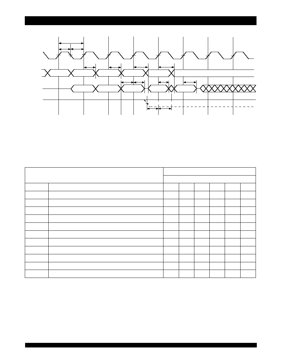
Control Interface Timing Waveform
(1)
Control Interface Commands
(1)
NOTES:
1. This waveform describes the command interaction across the IOD Bus to the IDT77V400 Switching Memory.
2. The result of this GET STATUS command is that an ISAM is full and ready to be stored to the Fusion Memory of the IDT77V400.
NOTES:
1. CMD bus commands not defined in this table are undefined and are not implemented by the IDT77V500.
2. "x" represents the specific ISAM or OSAM being accessed (IP0-IP7 or OP0-OP7 respectively).
3. "n" represents the appropriate bit of the binary representation of the ISAM or OSAM being accessed (000 to 111).
GET
STATUS
STORE
ISAM
PUT
HEADER
GET
HEADER ISAM
GET
STATUS
SCLK
CRCERR
3607 drw 06
CMD0-5
IOD0-31
Input -
Old Header
[ CRC ERROR = LOW ]
Output -
New Header
[ AVAILABLE FOR NEXT COMMAND ]
Output -
Cell Addr
t
CYC
t
CH
t
CL
t
CDC
t
DCC
t
SIO
t
SCRC
t
HCRC
t
CDIO
t
DCIO
STATUS
STATUS
(2)
t
HIO
(2)
t
CDIO
t
DCIO
)
0
:
5
D
M
C
(
t
i
B
s
u
B
D
N
A
M
M
O
C
b
S
M
b
S
L
d
n
a
m
m
o
C
n
o
i
t
p
i
r
c
s
e
D
d
n
a
m
m
o
C
5
4
3
2
1
0
x
I
H
G
x
M
A
S
I
m
o
rf
r
e
d
a
e
H
t
e
G
)
2
(
0
0
1
n
)
3
(
n
)
3
(
n
)
3
(
T
S
G
s
ti
B
r
e
t
s
i
g
e
R
s
u
t
a
t
S
M
A
S
I
t
e
G
0
1
0
0
1
0
R
E
G
s
ti
B
r
e
t
s
i
g
e
R
r
o
r
r
E
t
e
G
0
1
0
1
1
0
x
E
T
S
x
M
A
S
I
n
i
ll
e
C
e
r
o
t
S
)
2
(
y
r
o
m
e
M
n
i
r
e
ff
u
B
ti
d
E
d
n
a
1
0
0
n
)
3
(
n
)
3
(
n
)
3
(
x
O
D
L
x
M
A
S
O
o
t
n
i
y
r
o
m
e
M
m
o
rf
ll
e
C
d
a
o
L
)
2
(
1
1
0
n
)
3
(
n
)
3
(
n
)
3
(
E
H
P
r
e
ff
u
B
ti
d
E
n
i
r
e
d
a
e
H
w
e
n
t
u
P
1
1
1
1
0
0
C
E
H
P
r
e
ff
u
B
ti
d
E
n
i
e
t
y
b
C
R
C
w
e
n
d
n
a
r
e
d
a
e
H
w
e
n
t
u
P
1
1
1
1
0
1
F
E
R
y
r
o
m
e
M
n
o
i
s
u
F
h
s
e
rf
e
R
0
1
0
1
1
1
C
D
L
r
e
t
s
i
g
e
R
n
o
it
a
r
u
g
if
n
o
C
d
a
o
L
1
1
1
0
1
0
E
H
O
r
e
t
s
i
g
e
R
ti
d
E
t
u
p
t
u
O
n
i
r
e
d
a
e
H
w
e
n
t
u
P
1
1
1
1
1
0
C
E
H
O
r
e
t
s
i
g
e
R
ti
d
E
t
u
p
t
u
O
n
i
e
t
y
b
C
R
C
w
e
n
d
n
a
r
e
d
a
e
H
w
e
n
t
u
P
1
1
1
0
0
1
0
1
l
b
t
7
0
6
3
6.42
IDT77V500 Preliminary
SWITCHStAR Switch Controller Industrial and Commercial Temperature Range
9
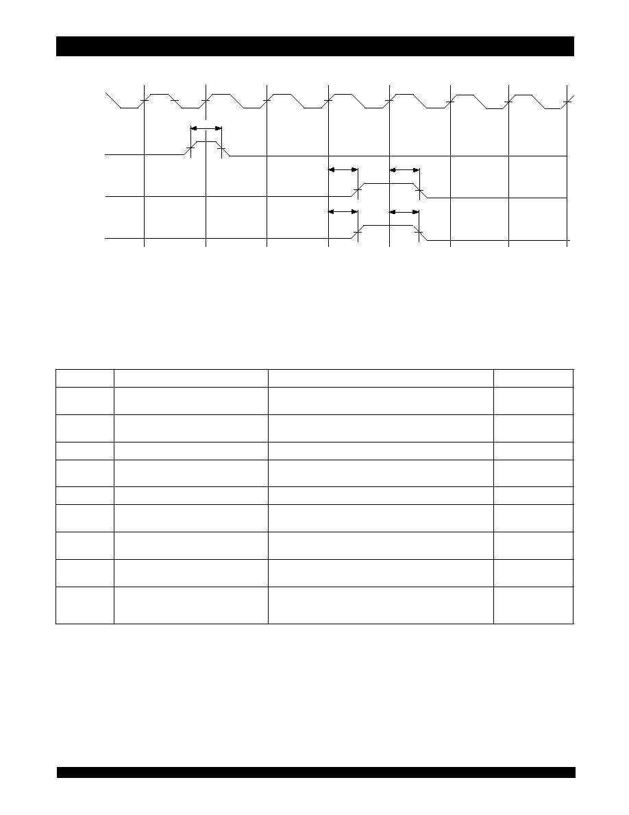
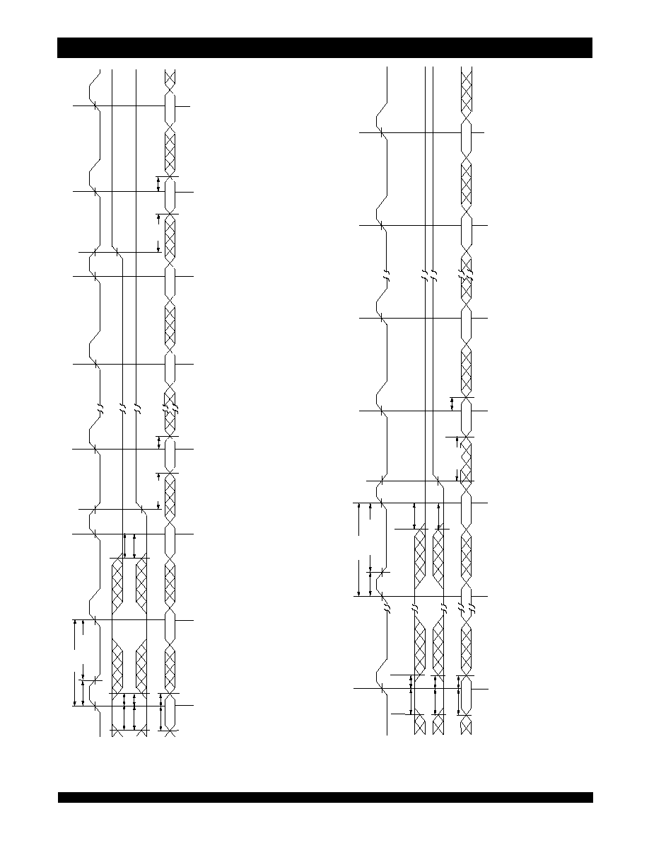
NOTE:
1. OFRM1-7 become CBUS1-7 (Outputs) during cell bus operations to arbitrate between multiple IDT77V500's.
SFRM, CBUS, and OFRM Timing Waveforms
Manager Commands
(1)
NOTE:
1. Manager Command codes not defined in this table are not to be used.
SCLK
OFRM
3607 drw 07
t
OFP
OFRM/CBUS
t
CDOF
t
DCOF
(1)
SFRM
t
DCS
t
CDS
d
n
a
m
m
o
C
e
m
a
N
d
n
a
m
m
o
C
n
o
i
t
p
i
r
c
s
e
D
d
n
a
m
m
o
C
)
x
e
H
n
i
(
e
d
o
C
L
S
R
W
y
r
o
m
e
M
k
n
i
L
e
c
i
v
r
e
S
e
ti
r
W
e
c
i
v
r
e
s
d
e
l
u
d
e
h
c
s
e
z
il
a
it
i
n
i
o
t
y
r
o
m
e
M
k
n
i
L
e
c
i
v
r
e
S
o
t
n
i
e
ti
r
W
.
s
t
s
il
3
0
T
A
T
S
s
u
t
a
t
s
0
0
5
V
7
7
T
D
I
d
a
e
R
n
o
it
a
m
r
o
f
n
i
e
l
b
a
li
a
v
A
.
0
0
5
V
7
7
T
D
I
e
h
t
f
o
s
u
t
a
t
s
l
a
n
r
e
t
n
i
e
h
t
s
d
a
e
R
.
s
t
n
u
o
c
d
n
a
s
r
e
t
s
i
g
e
r
r
o
r
r
e
s
u
o
ir
a
v
s
e
d
u
l
c
n
i
7
0
G
F
C
D
L
s
ti
B
n
o
it
a
r
u
g
if
n
o
C
0
0
4
V
7
7
T
D
I
d
a
o
L
.
0
0
4
V
7
7
T
D
I
e
h
t
o
t
n
o
it
a
m
r
o
f
n
i
n
o
it
a
r
u
g
if
n
o
c
s
e
s
s
a
P
8
0
P
U
S
p
u
t
e
s
ll
a
C
C
V
r
e
P
e
h
t
f
o
y
rt
n
e
n
a
o
t
n
i
n
o
it
a
m
r
o
f
n
i
e
t
a
ir
p
o
r
p
p
a
e
h
t
s
e
ti
r
W
.
n
o
it
c
n
u
f
p
u
t
e
s
ll
a
c
e
h
t
m
r
o
f
r
e
p
o
t
y
r
o
m
e
M
9
0
T
N
I
0
0
5
V
7
7
T
D
I
e
z
il
a
it
i
n
I
.
0
0
5
V
7
7
T
D
I
e
h
t
f
o
s
r
e
t
s
i
g
e
r
n
o
it
a
r
u
g
if
n
o
c
l
a
n
r
e
t
n
i
e
h
t
s
e
z
il
a
it
i
n
I
A
0
L
E
S
0
0
5
V
7
7
T
D
I
a
t
c
e
l
e
S
e
c
i
v
e
d
e
l
p
it
l
u
m
a
n
i
d
e
l
b
a
n
e
e
b
o
t
0
0
5
V
7
7
T
D
I
e
h
t
s
t
c
e
l
e
S
.
n
o
it
a
r
u
g
if
n
o
c
B
0
T
R
A
T
S
n
o
it
a
z
il
a
it
i
n
I
0
0
5
V
7
7
T
D
I
f
o
d
n
E
n
e
e
b
s
a
h
ti
r
e
tf
a
e
t
a
t
s
d
e
l
b
a
n
e
n
a
o
t
n
i
0
0
5
V
7
7
T
D
I
e
h
t
s
t
e
S
.
d
e
z
il
a
it
i
n
i
C
0
R
B
C
r
e
l
u
d
e
h
c
S
R
B
C
a
p
u
t
e
S
e
t
a
R
ti
B
t
n
a
t
s
n
o
C
e
h
t
n
i
t
s
il
e
c
i
v
r
e
s
t
u
p
t
u
o
d
e
t
c
e
l
e
s
a
p
u
s
t
e
S
.
e
d
o
m
)
R
B
C
(
D
0
M
R
A
P
s
r
e
t
e
m
a
r
a
P
t
e
S
w
o
l
P
L
C
e
h
t
g
n
i
d
u
l
c
n
i
,
0
0
5
V
7
7
T
D
I
e
h
t
n
i
s
r
e
t
e
m
a
r
a
p
s
u
o
ir
a
v
s
t
e
S
r
e
t
a
w
w
o
l
D
P
E
e
h
t
d
n
a
,
k
r
a
m
r
e
t
a
w
w
o
l
I
C
F
E
e
h
t
,
k
r
a
m
r
e
t
a
w
.
k
r
a
m
E
0
1
1
l
b
t
7
0
6
3
6.42
IDT77V500 Preliminary
SWITCHStAR Switch Controller Industrial and Commercial Temperature Range
10
M
ana
ger Bus R
ead
Ti
m
i
ng
W
a
v
e
f
o
r
m
(1
)
Mana
ger
Bus Wr
i
t
e Ti
m
i
ng W
a
v
e
f
o
r
m
(1
)
NOTES:
1
.
Write operations, both for Commands and Data, are synchronous to the rising edge of
MSTRB
. The data placed on the MDATA pins is determined by the state of the MD/
C
pin.
2
.
Either a Read cycle was completed or a Status Acknowledge was executed immediately prior to the first
MSTRB
of this write waveform.
3
.
The combination of
MSTRB
Low and MR/
W
High (Read mode) asynchronously enables the MDATA pins as outputs.
The data placed on the MDATA pins is determined by the state of the MD/
C
pin.
4
.
After the Command is written, the Manager must take MR/
W
High (Read mode) to wait for a valid Command Acknowledge from the IDT77V500 before proceeding. Reading a High Bit 7 of the sta
tus register under these
conditions indicates the command has been acknowledged by the IDT77V500. This may take multiple IDT77V500 SCLK cycles based on
possible higher priority operations that the IDT77V500 must support.
5
.
A valid Acknowledge from the IDT77V500 is indicated by a High Command Acknowledge bit (Bit 7 of the Status Register).
MD/
C
MSTRB
MR/
W
3607 drw 08
t
SMRW
t
HMRW
t
SMD
t
HMD
MDATA
t
MCH
t
MCL
t
MCYC
t
SM
t
HM
Write first
8 ADDR bits
Acknowledge Read
t
AMD
DATA
OUT
DATA
OUT
CMD
IN
ADDR
IN
ADDR
IN
t
OHMD
Write last
8 ADDR bits
Write Cycle-
Read Command
(2)
(3)
DATA
OUT
DATA
OUT
DATA
OUT
(4)
Read Byte 0
Acknowledge Read
Acknowledge Read
Valid Command Acknowledge
t
AMD
t
OHMD
t
SMRW
t
SM
Read Byte 1
(5)
MDATA
MSTRB
t
SM
t
HM
3607 drw 09
t
SMRW
t
HMRW
t
SMD
t
HMD
MR/
W
MD/
C
t
MCH
t
MCL
t
MCYC
DATA
IN
DATA
IN
CMD
IN
DATA
OUT
Write Data Byte 0
Write Data Byte 12
Write Cycle-
Write Command
Acknowledge Read
t
OHMD
T0
T12
t
AMD
DATA
OUT
(3)
(4)
Acknowledge Read
DATA
OUT
DATA
OUT
(5)
Acknowledge Read
Acknowledge Read
Valid Command Acknowledge
t
SM
t
SMRW
(2)
NOTES:
1
.
Write operations, both for Commands and Data, are synchronous to the rising edge of
MSTRB
. The data placed on the MDATA pins is determined by the state of the MD/
C
pin.
2
.
The combination of
MSTRB
Low and MR/
W
High (Read mode) asynchronously enables the MDATA pins as outputs. That is, data is available to be read one asynchronous t
AMD
time after the falling edge of
MSTRB
if MR/
W
is HIGH.
3
.
After the Command is written, the Manager must take MR/
W
High (Read mode) to wait for a valid Command Acknowledge from the IDT77V500 before proceeding. Reading a High Bit 7 of the sta
tus register under these
conditions indicates the command has been acknowledged by the IDT77V500. This may take multiple IDT77V500 SCLK cycles based on
possible higher priority operations that the IDT77V500 must support.
4
.
A valid Acknowledge from the IDT77V500 is indicated by a High Command Acknowledge bit (Bit 7 of the Status Register).
5
.
Waveform illustrates first two bytes of data only. Additional bytes may be available based on command used.
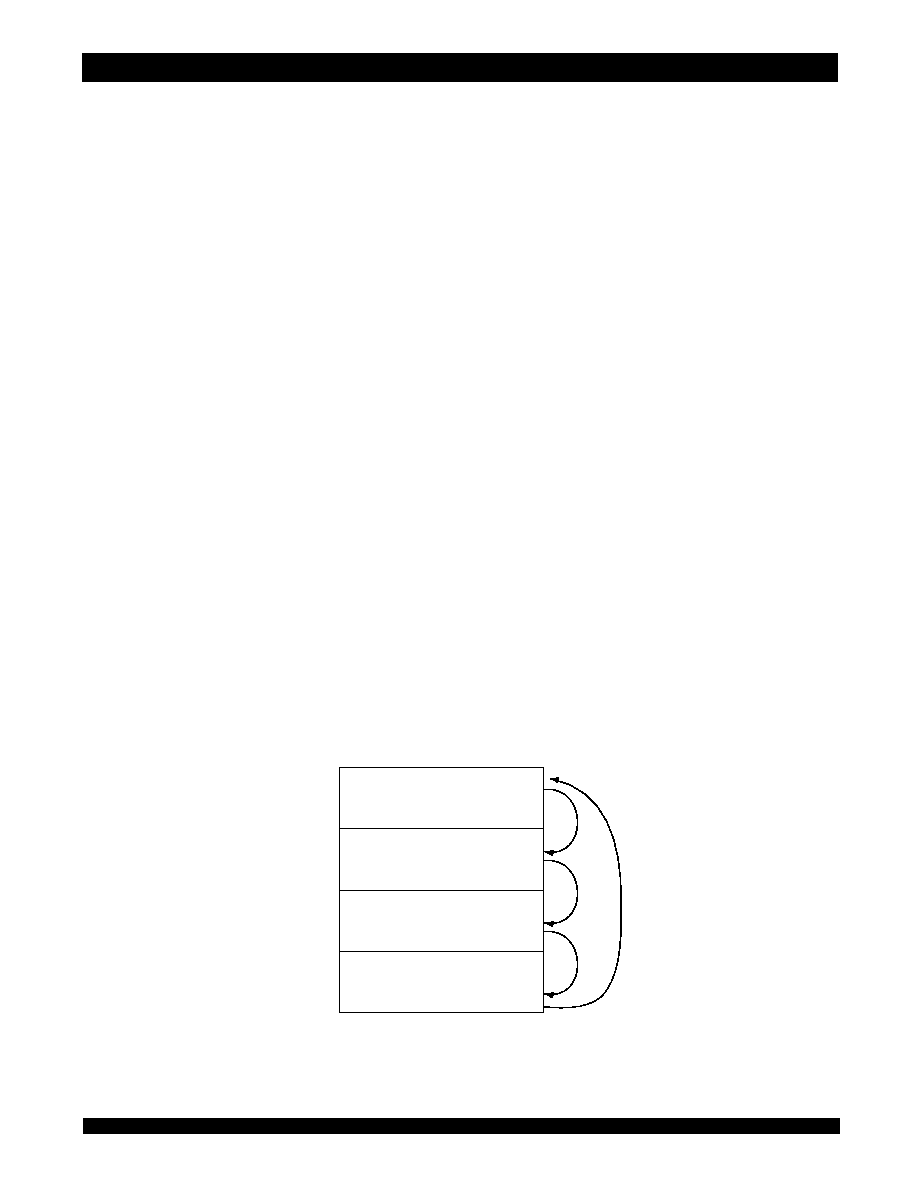
6.42
IDT77V500 Preliminary
SWITCHStAR Switch Controller Industrial and Commercial Temperature Range
11
The Constant Bit Rate (CBR) functionality of the IDT77V500
provides both the opportunity for scheduling priority traffic at a regular
interval and traffic shaping capability. Two external CBR clocks,
CBRCLK3 and CBRCLK2, are available and associated with Output
Priority 3 (Highest Priority) and Priority 2 respectively. Calls assigned
to a particular CBR VC in the IDT77V500 Per VC Table are linked
together in a CBR Per VC list by output, so that a cell from each VC
of a particular CBR Per VC list are serviced on each cycle through the
list. The CBR Per VC List is identified by both the output and CBR
priority on that output; for example, OPyCBRx VC list represents
Output y (Output number 0-7) and CBR priority x (CBR priority 3 or 2).
Figure 3 is an example of an OPyCBRx VC List with four VCs in the
list: 100 (the first entry in the list), 200, 300 and 400. The arrows
indicate the linking sequence in this VC List. Figure 3 will be used with
the CBR Clock Functional Waveforms to illustrate two basic functional
implementations using the CBR Clocks.
CBR Clock Functional Waveform Example 1 uses the
CBR clocks to frame execution of the OPyCBRx VC List. A cell from
a specific VC on the OPyCBRx VC List is scheduled on each rising
clock edge of SCLK after a falling edge of CBRCLKx. The cell will then
be transmitted when output y is available and other previously
scheduled Input and Output ports of the IDT77V400 have been
serviced. This delay can be as long as 65 SCLK cycles maximum for
each cell in the CBR VC List , although it will typically be significantly
less. This delay needs to be taken into account, as the next cell in the
OPyCBRx VC List will not be scheduled until the previous cell in the
list has been serviced. Thus enough CBRCLKx pulses need to be
provided to make sure all potential cells in the OPyCBRx VC List are
CBR Functional Description
Figure 3.
OPyCBRx VC List Example
scheduled. This waveform illustrates the ideal case of each cell being
immediately transmitted after scheduling, enabling the scheduling
and transmission of the next cell in the OPyCBRxVC List on the next
SCLK rising edge. CBRCLKx HIGH for eight SCLK cycles or more
tells the controller that the pointer should be moved back to the top of
the CBR VC List if all the VCs in the list have been serviced. Thus the
user can establish a frame duration and be assured that a cell from
each VC in the OPyCBRx VC List is transmitted in each frame time.
Sub lists can also be established within the CBR VC List so that a
particular VC could be weighted to ship more cells per frame than the
others.
Example 2 illustrates using very slow CBR clocks (tCHx greater
than or equal to 8 SCLKs) toshape traffic in a VBR form of implemen-
tation. A cell from a VC on the OPyCBRx VC List is again scheduled
on each rising clock edge of SCLK after a falling edge of CBRCLKx,
but since t
CH
x is HIGH for more than eight SCLKs, there is more direct
control over the exact time in which each cell of the VC List is
scheduled. The single cell will then be transmitted when the output is
available and other previously scheduled Input and Output ports of the
IDT77V400 have been serviced (there is again the potential 65 SCLK
delay based on other traffic passing through the IDT77V400). The
IDT77V500 will service all of the VCs in the OPyCBRx VC List
because the count will prevent the pointer from returning to the top of
the CBR VC List until all VCs on the list with cells have been serviced.
The user can thus more closely manage the transmission of cells with
this slower CBR clock rate because it is more directly related to
individual CBRCLKx High-to-Low transitions.
3607 drw 10
100
200
300
400
Beginning
End
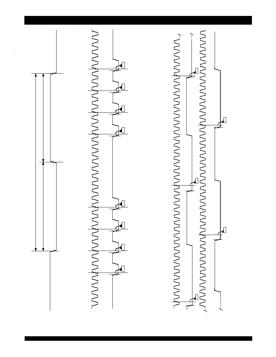
6.42
IDT77V500 Preliminary
SWITCHStAR Switch Controller Industrial and Commercial Temperature Range
12
NOTES:
1. This example shows the procedure recommended for use of direct CBR scheduling. "x" for this waveform represents either 2 or 3, depending on which CBRCLK is used (CBRCLK2 or CBRCLK3)
("y" represents the specific output (0-7)). The OPyCBRx VC List for this example is defined in figure 3.
2. A cell from a VC on the OPyCBRx VC List is scheduled on each rising clock edge of SCLK after a falling edge of CBRCLKx.
3. This example shows four VC's in the OPyCBRx VC List. The number of VC's in the OPxCBRx VC List may be as large as 8192.
4. The period between reinitiation of the OPyCBRx VC List defines the frame size; that is, the amount of time between starting the transmissions from the top of the OPyCBRx VC List.
CBRCLKx must be HIGH for eight clocks or more to reinitiate the transmission sequence at the start of the OPyCBRx VC List.
CBR Clock Functional Waveform Example 2 - VBR/CBR Implementation (t
CH
x > 8 SCLK)
(1)
CBR Clock Parameters
(1)
CBR Clock Functional Waveform Example 1 - CBR Frame Implementation (Fast CBRCLK with
Frame Timing)
(1)
NOTES:
1. This example shows the use of a slower CBRCLK (t
CH
x > 8 SCLK) to provide VBR/CBR traffic shaping. For this waveform "x" represents either 2 or 3, depending on which CBRCLK is used
(CBRCLK2 or CBRCLK3). ("y" represents the specific output (0-7)) The OPyCBRx VC List for this example is defined in Figure 3.
2. A cell from a VC on the OPyCBRx VC List is scheduled on each rising edge of SCLK after a falling edge of CBRCLKx.
3. t
CH
x
>
8 SCLK so that a cell is scheduled after each falling edge of CBRCLKx.
4. The pointer has moved back to the beginning of the OPyCBRx VC List.
NOTES:
1. "x" for this waveform represents either 2 or 3, depending on which CBRCLK is used (CBRCLK2 or CBRCLK3).
CBRCLKx
t
CLx
t
CHx
t
CYCx
3607 drw 11
(2)
(3)
SCLK
CBRCLKx
100
200
300
400
(4)
100
200
300
400
(2)
(3)
3607 drw 12
100
SCLK
(3)
cont'd
waveform
CBRCLKx
(2)
see cont'd
waveform
3607 drw 13
(4)
200
300
100
400
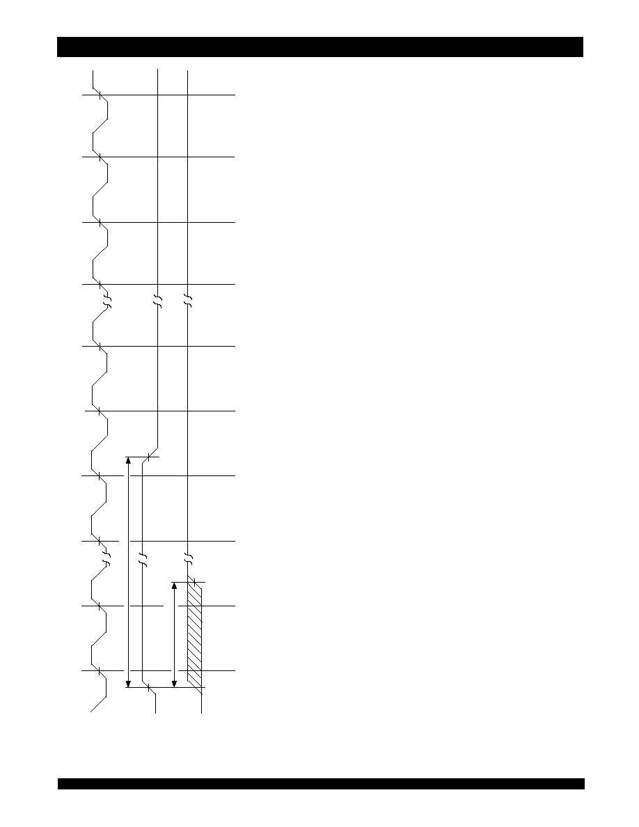
6.42
IDT77V500 Preliminary
SWITCHStAR Switch Controller Industrial and Commercial Temperature Range
13
Re
s
e
t
Wave
fo
r
m
S
NOTES:
1
.
RESETI must be held HIGH
for 8 SCLK cycles. When RESETI goes
LOW again 8191 cycles are used prior to the
Status Acknowledge bits showing the internal reset process is complete.
2
.
This delay should typically be much less than two SCLK cycles. RESETO remains HIGH until START Command is received from the C
all Setup Manager.
SCLK
RESETI
3607 drw 14
1
27812
8190
8191
1
t
RSI
RESETO
(1)
(2)
2
2 clock cycles max.
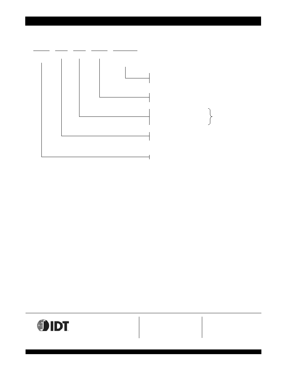
6.42
IDT77V500 Preliminary
SWITCHStAR Switch Controller Industrial and Commercial Temperature Range
14
Ordering Information
A
Power
99
Speed
A
Package
A
Process/
Temperature
Range
Blank
I
Commercial (0
∞
C to +70
∞
C)
Industrial (-40
∞
C to +85
∞
C)
PF
100-pin TQFP (PK100-1)
27
25
S
Standard Power
XXXXX
Device
Type
ATM Cell Based Switch Controller
77V500
IDT
3607 drw 15
System Clock Period in ns
Commercial & Industrial
SWITCHStAR and the IDT logo are registered trademarks of Integrated Device Technology, Inc.
CORPORATE HEADQUARTERS
for SALES:
for Tech Support:
2975 Stender Way
800-345-7015 or 408-727-6116
831-754-4613
Santa Clara, CA 95054
fax: 408-492-8674
SWITCHStARhelp@idt.com
www.idt.com
Preliminary Datasheet:
Definition
"PRELIMINARY" datasheets contain descriptions for products that are in early release.
Datasheet Document History
3/1/99:
Updated to new format.
Added Industrial Specifications.
Added S25 Speed Grade.
Pg. 3
Package Diagram noes added for clarification.
Pg. 4
Pin description table descriptions corrected. OFRM and Vss pin number corrections made.
Pg. 5
V
TERM
in Maximum ratings table reduced to 3.9V.
Pg. 10
Manager Bus Sequence Waveforms Figures 9 and 10 and their notes modified for clarity.
Pg. 14
Updated Ordering Information for S156 speed grade and Industrial temperature product. Added Preliminary
Datasheet definition and Datasheet Document History.