1
IDTQS32XR245
HIGH-SPEED CMOS QUICKSWITCH 16-BIT LOW RESISTANCE BUS SWITCH
INDUSTRIAL TEMPERATURE RANGE
NOVEMBER 1999
1999 Integrated Device Technology, Inc.
DSC-5545/2
c
IDTQS32XR245
INDUSTRIAL TEMPERATURE RANGE
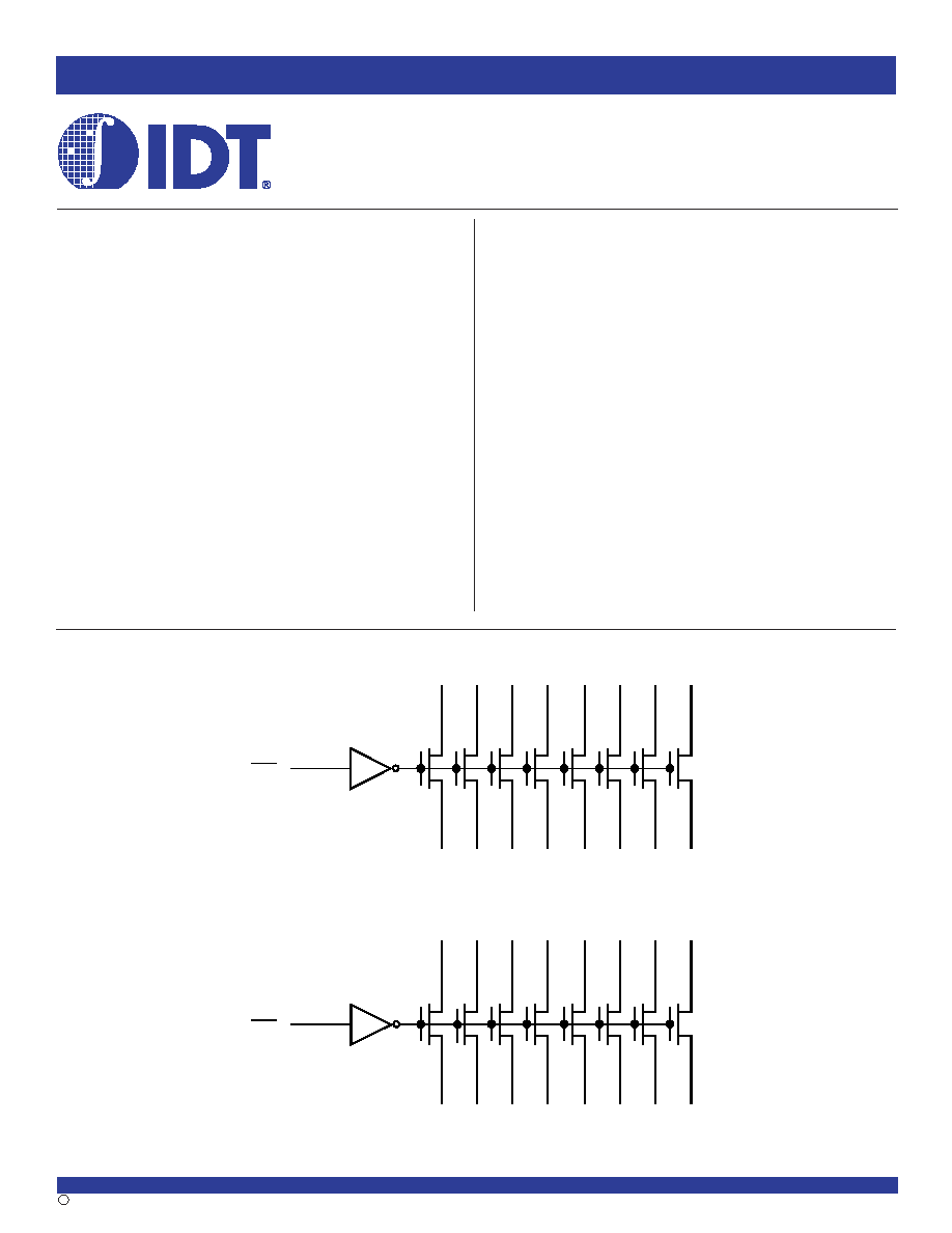
FUNCTIONAL BLOCK DIAGRAM
The IDT logo is a registered trademark of Integrated Device Technology, Inc.
FEATURES:
∑ Enhanced N channel FET with no inherent diode to Vcc
∑ 2.5
bidirectional switches connect inputs to outputs
∑ Zero propagation delay, zero ground bounce
∑ QS32XR245 is a 16-bit version of QS3R245
∑ Flow-through pinout for easy layout
∑ Undershoot clamp diodes on all switch and control inputs
∑ TTL-compatible control inputs
∑ Available in 40-pin QVSOP package
APPLICATIONS:
∑ Low resistance applications
∑ Hot-swapping, hot-docking (low resistance for PCI and
Compact PCI applications)
∑ Voltage translation (5V to 3.3V)
∑ Capacitance reduction and isolation
∑ Power conservation
∑ Logic replacement (data processing)
∑ Clock gating
QUICKSWITCH
Æ
PRODUCTS
HIGH-SPEED CMOS QUICKSWITCH
16-BIT LOW RESISTANCE
MULTIWIDTH
TM
BUS SWITCH
DESCRIPTION:
The QS32XR245 is a member of the MultiWidth
TM
family of QuickSwitch
devices and provides a set of 32 high-speed low resistance CMOS
compatible bus switches in a flow-thru pinout. This device is available in the
MillipaQ package, the world's first small outline 16-bit solution. The low on-
resistance of the QS32XR245 allows inputs to be connected to outputs
without adding propagation delay and without generating additional ground
bounce noise. When Output Enable (OEn) is low, the switches are turned
on, connecting bus A to bus B. When OEn is high, the switches are turned
off. This device is ideally suited for 16/32 bit applications where board space
is at a premium.The low resistance of QS32XR245 makes it ideal for PCI
hot docking application.
QuickSwitch devices provide an order of magnitude faster speed than
conventional logic devices.
The QS32XR245 is characterized for operation at -40∞C to +85∞C.
B
0
O E
1
A
0
B
1
A
1
B
2
A
2
B
3
A
3
B
4
A
4
B
5
A
5
B
6
A
6
B
7
A
7
B
8
O E
2
A
8
B
9
A
9
B
10
A
10
B
11
A
11
B
12
A
12
B
13
A
13
B
14
A
14
B
15
A
15
2
INDUSTRIAL TEMPERATURE RANGE
IDTQS32XR245
HIGH-SPEED CMOS QUICKSWITCH 16-BIT LOW RESISTANCE BUS SWITCH
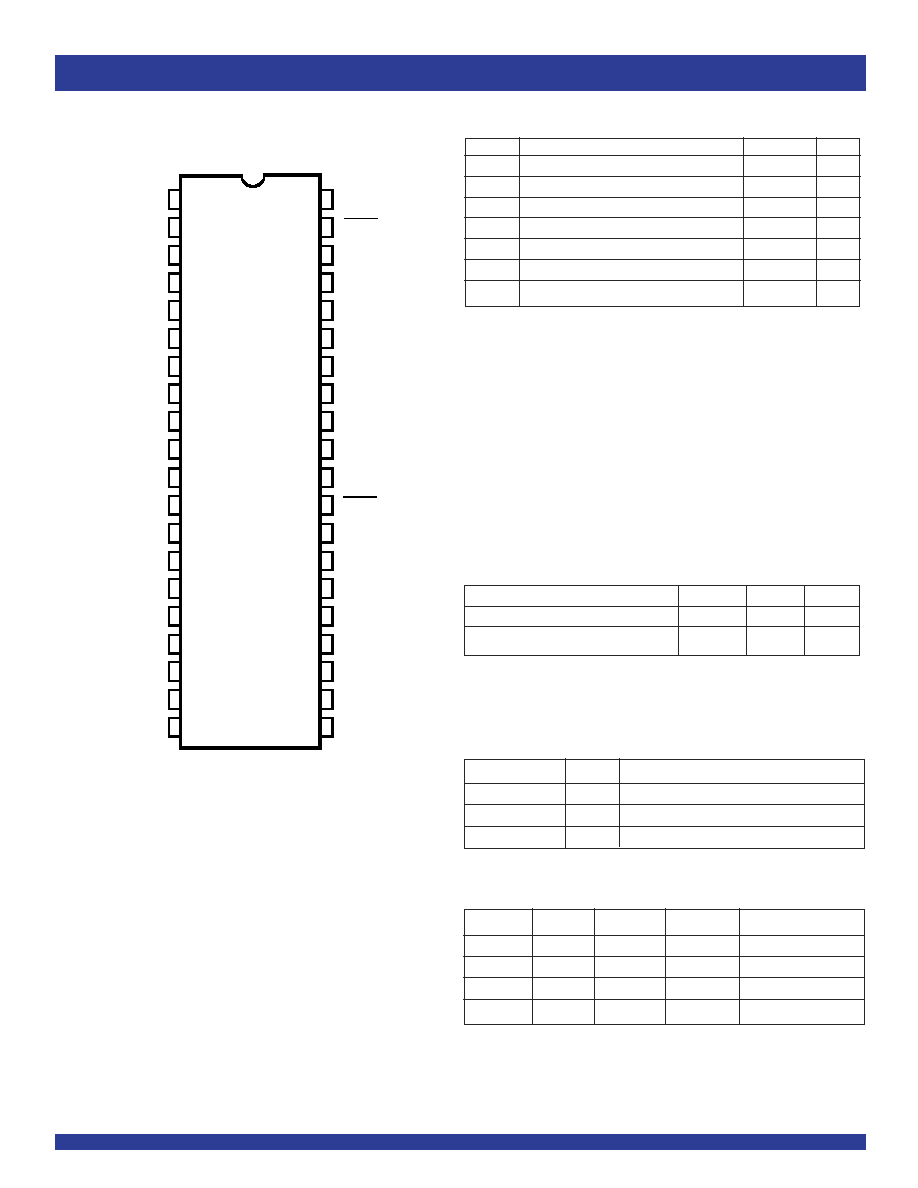
PIN CONFIGURATION
NOTE:
1. H = HIGH Voltage Level
L = LOW Voltage Level
Z = High-Impedance
FUNCTION TABLE
(1)
CAPACITANCE
(T
A
= +25∞C, f = 1.0MH
Z
, V
IN
= 0V, V
OUT
= 0V)
NOTE:
1. This parameter is measured at characterization but not tested.
Pins
Typ.
Max.
(1)
Unit
Control Pins
3
4
pF
Quickswitch Channels (Switch OFF)
5
6
pF
Symbol
Description
Max
Unit
V
TERM
(2)
Supply Voltage to Ground
≠0.5 to +7
V
V
TERM
(3)
DC Switch Voltage Vs
≠0.5 to +7
V
V
TERM
(3)
DC Input Voltage V
IN
≠0.5 to +7
V
V
AC
AC Input Voltage (pulse width
20ns)
≠3
V
I
OUT
DC Output Current
120
mA
P
MAX
Maximum Power Dissipation (T
A
= 85∞C)
0.92
W
T
STG
Storage Temperature
≠65 to +150
∞C
ABSOLUTE MAXIMUM RATINGS
(1)
NOTE:
1. Stresses greater than those listed under ABSOLUTE MAXIMUM RATINGS may cause
permanent damage to the device. This is a stress rating only and functional operation
of the device at these or any other conditions above those indicated in the operational
sections of this specification is not implied. Exposure to absolute maximum rating
conditions for extended periods may affect reliability.
2. Vcc terminals.
3. All terminals except Vcc.
QVSOP
TOP VIEW
PIN DESCRIPTION
Pin Names
I/O
Description
OE1, OE2
I
Output Enable
An
I/O
Bus A
Bn
I/O
Bus B
OE1
OE2
A
0
- A
7
A
8
- A
15
Function
H
H
Z
Z
Disconnect
L
H
B
0
- B
7
Z
Connect
H
L
Z
B
8
- B
15
Connect
L
L
B
0
- B
7
B
8
- B
15
Connect
40
39
38
37
36
35
34
33
32
31
30
29
28
27
26
25
24
23
22
21
O E1
B
0
B
1
B
2
B
3
B
4
B
5
B
6
B
7
V
C C
O E2
B
8
B
9
B
10
B
11
B
12
B
13
B
14
B
15
V
C C
1
2
3
4
5
6
7
8
9
10
11
12
13
14
15
16
17
18
19
20
NC
A
0
A
1
A
2
A
3
A
4
A
5
A
6
A
7
G ND
NC
A
8
A
9
A
10
A
11
A
12
A
13
A
14
A
15
G ND
3
IDTQS32XR245
HIGH-SPEED CMOS QUICKSWITCH 16-BIT LOW RESISTANCE BUS SWITCH
INDUSTRIAL TEMPERATURE RANGE
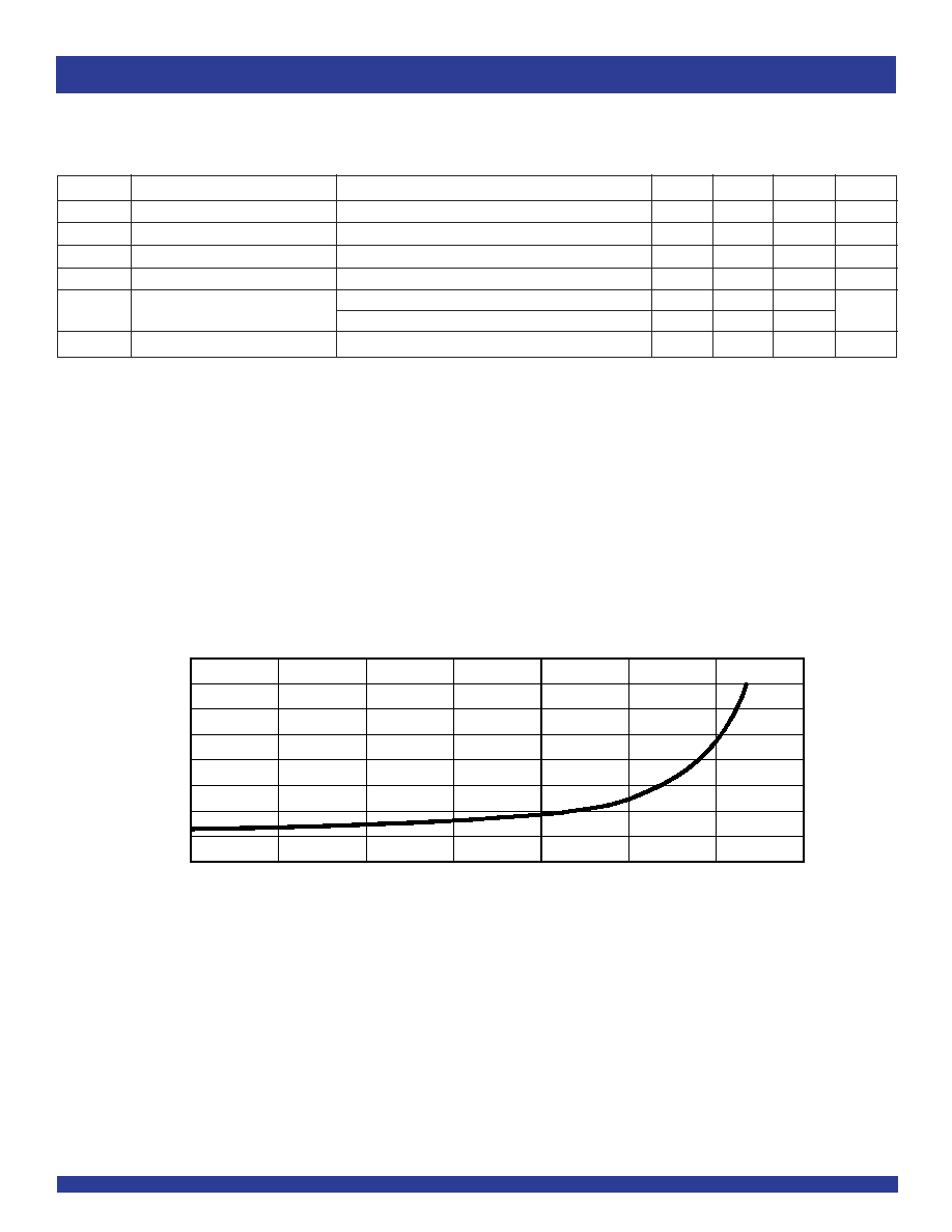
R
ON
(ohms)
V
IN
(Volts)
TYPICAL ON RESISTANCE vs V
IN
AT V
CC
= 5V
Symbol
Parameter
Test Conditions
Min.
Typ.
(1)
Max.
Unit
V
IH
Input HIGH Level
Guaranteed Logic HIGH for Control Pins
2
--
--
V
V
IL
Input LOW Level
Guaranteed Logic LOW for Control Pins
--
--
0.8
V
I
IN
Input LeakageCurrent (Control Inputs)
0V
V
IN
V
CC
--
--
±1
µA
I
OZ
Off-State Output Current (Hi-Z)
0V
V
OUT
V
CC
, Switches OFF
--
--
±1
µA
R
ON
Switch ON Resistance
(2)
V
CC
= Min., V
IN
= 0V, I
ON
= 30mA
--
2.5
5
V
CC
= Min., V
IN
= 2.4V, I
ON
=15mA
--
4
8.5
V
P
Pass Voltage
(3)
V
IN
= V
CC
= 5V, I
OUT
= -5
µA
3.7
4
4.3
V
DC ELECTRICAL CHARACTERISTICS OVER OPERATING RANGE
Following Conditions Apply Unless Otherwise Specified:
Industrial: T
A
= ≠40∞C to +85∞C, V
CC
= 5.0V ±10%
NOTES:
1. Typical values are at V
CC
= 5.0V, T
A
= 25∞C.
2. Max value of R
ON
is guaranteed but not production tested.
3. Pass Voltage is guaranteed but not production tested.
16
14
12
10
8
6
4
2
0
0.0
0.5
1.0
1.5
2.0
2.5
3.0
3.5
4
INDUSTRIAL TEMPERATURE RANGE
IDTQS32XR245
HIGH-SPEED CMOS QUICKSWITCH 16-BIT LOW RESISTANCE BUS SWITCH
POWER SUPPLY CHARACTERISTICS
Symbol
Parameter
Test Conditions
(1)
Max.
Unit
I
CCQ
Quiescent Power Supply Current
V
CC
= Max., V
IN
= GND or Vcc, f = 0
6
µA
I
CC
Power Supply Current per Control Input HIGH
(2)
V
CC
= Max., V
IN
= 3.4V, f = 0
2.5
mA
I
CCD
Dynamic Power Supply Current per MHz
(3)
V
CC
= Max., A and B pins open
0.25
mA/MHz
Control Inputs Toggling at 50% Duty Cycle
NOTES:
1. For conditions shown as Min. or Max., use the appropriate values specified under DC Electrical Characteristics.
2. Per TLL driven input (V
IN
= 3.4V, control inputs only). A and B pins do not contribute to
Icc.
3. This current applies to the control inputs only and represents the current required to switch internal capacitance at the specified frequency. The A and B inputs generate no significant
AC or DC currents as they transition. This parameter is guaranteed but not production tested.
SWITCHING CHARACTERISTICS OVER OPERATING RANGE
T
A
= -40∞C to +85∞C, V
CC
= 5.0V ± 10%;
C
LOAD
= 50pF, R
LOAD
= 500
unless otherwise noted.
Symbol
Parameter
Min.
(1)
Typ.
Max.
Unit
t
PLH
Data Propagation Delay
(2,3)
--
--
0.12
ns
t
PHL
An to/from Bn
t
PZL
Switch Turn-on Delay
0.5
--
5.6
ns
t
PZH
OEn to An/Bn
t
PLZ
Switch Turn-off Delay
(2)
0.5
--
4.5
ns
t
PHZ
OEn to An/Bn
NOTES:
1.
Minimums are guaranteed but not production tested.
2.
This parameter is guaranteed but not production tested.
3.
The bus switch contributes no propagation delay other than the RC delay of the ON resistance of the switch and the load capacitance. The time constant for the switch alone
is of the order of 0.12ns for C
L
= 50pF. Since this time constant is much smaller than the rise and fall times of typical driving signals, it adds very little propagation delay to
the system. Propagation delay of the bus switch, when used in a system, is determined by the driving circuit on the driving side of the switch and its interaction with the load
on the driven side.
5
IDTQS32XR245
HIGH-SPEED CMOS QUICKSWITCH 16-BIT LOW RESISTANCE BUS SWITCH
INDUSTRIAL TEMPERATURE RANGE
ORDERING INFORMATION
CORPORATE HEADQUARTERS
for SALES:
for Tech Support:
2975 Stender Way
800-345-7015 or 408-727-6116
logichelp@idt.com
Santa Clara, CA 95054
fax: 408-492-8674
(408) 654-6459
www.idt.com
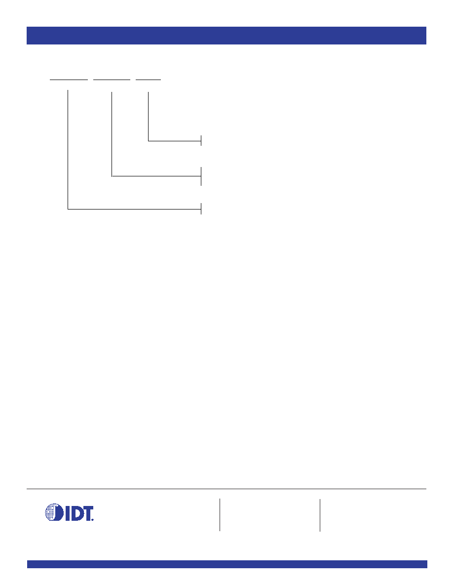
IDTQS
XXXXX
XX
Package
Device Type
Blank
Industrial (-40∞C to +85∞C)
40-Pin QVSOP
QVSOP - Green
Q2
Q2G
32XR245 High Speed CMOS Quickswitch 16-Bit Low Resistance
MultiWidth Bus Switch
X
Process