 | –≠–ª–µ–∫—Ç—Ä–æ–Ω–Ω—ã–π –∫–æ–º–ø–æ–Ω–µ–Ω—Ç: IDTQS3388 | –°–∫–∞—á–∞—Ç—å:  PDF PDF  ZIP ZIP |
1
IDTQS3388
HIGH-SPEED CMOS BUS EXCHANGE SWITCH WITH ACTIVE TERMINATION
INDUSTRIAL TEMPERATURE RANGE
APRIL 2000
2000 Integrated Device Technology, Inc.
DSC-5765/1
c
INDUSTRIAL TEMPERATURE RANGE
FEATURES:
∑ Enhanced N channel FET with no inherent diode to Vcc
∑ 5
bidirectional switches connect inputs to outputs
∑ Active termination drives bus pins to rails when switches are
off
∑ Zero propagation delay, zero added ground bounce
∑ Undershoot clamp diodes on all switch and control inputs
∑ Bus exchange allows nibble swap
∑ TTL-compatible input and output levels
∑ Bus-hold eliminates floating bus lines and reduces static
power consumption
∑ Available in QSOP package
The IDT logo is a registered trademark of Integrated Device Technology, Inc.
APPLICATIONS:
∑ Resource sharing
∑ Crossbar switching
∑ Last value latch (graphics and DSP)
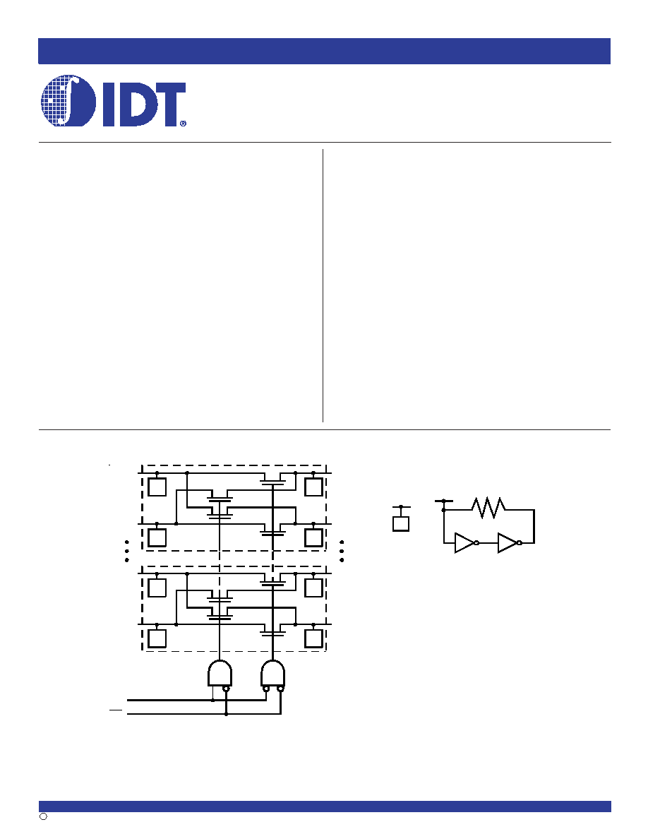
IDTQS3388
FUNCTIONAL BLOCK DIAGRAM
QUICKSWITCH
Æ
PRODUCTS
HIGH-SPEED CMOS BUS EXCHANGE
SWITCH WITH ACTIVE TERMINATION
(BUS HOLD)
DESCRIPTION:
The QS3388 provides ten high-speed CMOS TTL-compatible bus
switches with active terminators on the bus switch I/O pins. The low ON
resistance (5
) of the 3388 allows inputs to be connected to outputs without
adding propagation delay and without generating additional ground bounce
noise. When the switches are turned off, a low drive active terminator circuit
drives the disconnected pins to V
CC
or ground, away from the TTL threshold.
This prevents undriven buses from floating. The Bus Enable (BE) signal
turns the switches on. The Bus Exchange (BX) signal provides nibble swap
of the AB and CD pairs of signals. This exchange configuration allows byte
swapping of buses in systems. It can also be used as a five-wide 2-to-1
multiplexer and to create low delay barrel shifters, etc.
The QS3388 is characterized for operation at -40∞C to +85∞C.
A
4
C
4
D
4
B
4
B X
B E
A
0
C
0
D
0
B
0
T
T
T
T
T
T
T
T
T
=
R
2
INDUSTRIAL TEMPERATURE RANGE
IDTQS3388
HIGH-SPEED CMOS BUS EXCHANGE SWITCH WITH ACTIVE TERMINATION
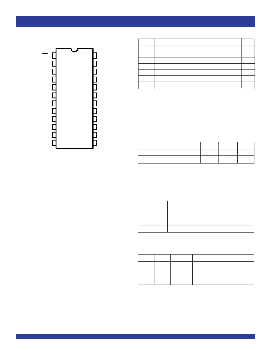
PIN CONFIGURATION
Symbol
Description
Max
Unit
V
TERM
(2)
Supply Voltage to Ground
≠0.5 to +7
V
V
TERM
(3)
DC Switch Voltage V
S
≠0.5 to +7
V
V
TERM
(3)
DC Input Voltage V
IN
≠0.5 to +7
V
V
AC
AC Input Voltage (pulse width
20ns)
≠3
V
I
OUT
DC Output Current
120
mA
P
MAX
Maximum Power Dissipation (T
A
= 85∞C)
0.5
W
T
STG
Storage Temperature
≠65 to +150
∞C
ABSOLUTE MAXIMUM RATINGS
(1)
NOTE:
1. H = HIGH Voltage Level
L = LOW Voltage Level
X = Don't Care
Z = High-Impedance
BE
BX
A
0
- A
4
B
0
- B
4
Function
H
X
Hi-Z
Hi-Z
Disconnect
L
L
C
0
- C
4
D
0
- D
4
Connect
L
H
D
0
- D
4
C
0
- C
4
Exchange
FUNCTION TABLE
(1)
Pins
Typ.
Max.
(1)
Unit
Control Inputs
3
5
pF
Quickswitch Channels (Switch OFF)
5
7
pF
CAPACITANCE
(T
A
= +25∞C, f = 1MHz, V
IN
= 0V, V
OUT
= 0V)
NOTE:
1. This parameter is guaranteed but not production tested.
Pin Names
I/O
Description
A
0
- A
4
, B
0
- B
4
I/O
A and B Buses
C
0
- C
4
, D
0
- D
4
I/O
C and D Buses
BE
I
Bus Switch Enable
BX
I
Bus Exchange
PIN DESCRIPTION
NOTES:
1. Stresses greater than those listed under ABSOLUTE MAXIMUM RATINGS may cause
permanent damage to the device. This is a stress rating only and functional operation
of the device at these or any other conditions above those indicated in the operational
sections of this specification is not implied. Exposure to absolute maximum rating
conditions for extended periods may affect reliability.
2. V
CC
terminals.
3. All terminals except V
CC
.
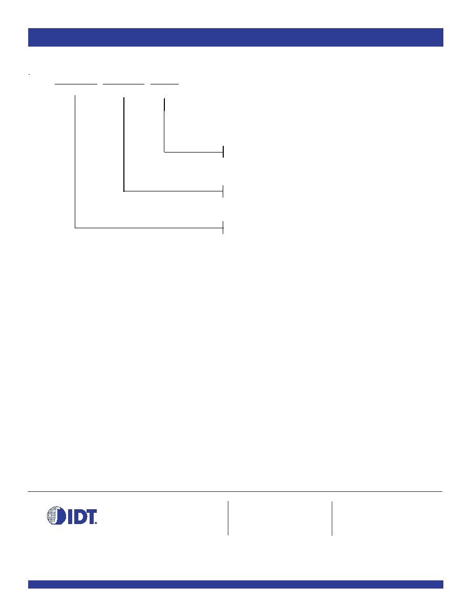
1
2
3
4
5
6
7
8
9
10
11
12
24
23
22
21
20
19
18
17
16
15
14
13
BE
C
0
A
0
B
0
D
0
C
1
A
1
B
1
D
1
C
2
A
2
GND
V
CC
D
4
B
4
A
4
C
4
D
3
B
3
A
3
C
3
D
2
B
2
BX
QSOP
TOP VIEW
3
IDTQS3388
HIGH-SPEED CMOS BUS EXCHANGE SWITCH WITH ACTIVE TERMINATION
INDUSTRIAL TEMPERATURE RANGE
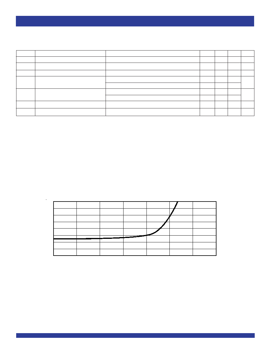
TYPICAL ON RESISTANCE vs V
IN
AT V
CC
= 5V
R
ON
(ohms)
V
IN
(Volts)
Symbol
Parameter
Test Conditions
Min.
Typ.
(1)
Max.
Unit
V
IH
Input HIGH Voltage
Guaranteed Logic HIGH for Control Pins
2
--
--
V
V
IL
Input LOW Voltage
Guaranteed Logic LOW for Control Pins
--
--
0.8
V
I
IN
Input Leakage Current (Control Inputs)
0V
V
IN
Vcc
--
.01
±1
µA
R
ON
Switch ON Resistance
Vcc = Min., V
IN
= 0V
, I
ON
= 30mA
--
6
8
Vcc = Min., V
IN
= 2.4V
, I
ON
= 15mA
--
12
17
I
BH
Input Current
(2)
Vcc = Max., V
IN
= 0V or Vcc
--
--
±20
µA
Switch Pins
Vcc = Max., 0.8V < V
IN
< 2V
--
--
±500
I
BHH
Bus Hold Sustaining Source Current - HIGH
(3)
Vcc = Min., V
IN
= 2V
≠
60
--
--
µA
I
BHL
Bus Hold Sustaining Sink Current - LOW
(4)
Vcc = Min., V
IN
= 0.8V
+ 60
--
--
DC ELECTRICAL CHARACTERISTICS OVER OPERATING RANGE
Following Conditions Apply Unless Otherwise Specified:
Industrial: T
A
= ≠40∞C to +85∞C, V
CC
= 5V ± 5%
16
14
12
10
8
6
4
2
0
0.0
0.5
1.0
1.5
2.0
2.5
3.0
3.5
NOTES:
1. Typical values are at V
CC
= 5.0V, T
A
= 25∞C.
2. Input current specified under two conditions:
a) Input voltage at GND or Vcc. This indicates the input current under steady-state condition.
b) Input voltage between 0.8V and 2V (TTL input threshold range). This indicates the maximum input current during transient condition. The driver connected to the input
must overcome this current requirement in order to switch the logic state of the bus-hold circuit.
3. I
BHH
represents the latching capability of the bus-hold circuit in logic HIGH state.
4. I
BHL
represents the latching capability of the bus-hold circuit in logic LOW state.
4
INDUSTRIAL TEMPERATURE RANGE
IDTQS3388
HIGH-SPEED CMOS BUS EXCHANGE SWITCH WITH ACTIVE TERMINATION
NOTES:
1. For conditions shown as Min. or Max., use the appropriate values specified under DC Electrical Characteristics.
2. Per TTL-driven input (V
IN
= 3.4V, control inputs only). A - D pins do not contribute to
Icc.
3. This current applies to the control inputs only and represents the current required to switch internal capacitance at the specified frequency. The A-D inputs generate no significant
AC or DC currents as they transition. This parameter is guaranteed but not production tested.
POWER SUPPLY CHARACTERISTICS
Symbol
Parameter
Test Conditions
(1)
Max.
Unit
I
CCQ
Quiescent Power Supply Current
V
CC
= Max., V
IN
= GND or V
CC
, f = 0
1.5
mA
I
CC
Power Supply Current per Input HIGH
(2)
V
CC
= Max., V
IN
= 3.4V, f = 0
2.5
mA
I
CCD
Dynamic Power Supply Current per MHz
(3)
V
CC
= Max., A - D Pins Open, Control Inputs Toggling @ 50% Duty Cycle
0.25
mA/MHz
SWITCHING CHARACTERISTICS OVER OPERATING RANGE
T
A
= -40∞C to +85∞C, V
CC
= 5V ± 5%
C
LOAD
= 50pF, R
LOAD
= 500
unless otherwise noted.
Symbol
Parameter
Min
.
(1)
Typ.
Max.
Unit
t
PLH
Data Propagation Delay
(2)
0.25
(3)
ns
t
PHL
AxBx to CxDx, CxDx to AxBx
t
PZL
Switch Turn-On Delay
1.5
6.5
ns
t
PZH
BE to Ax, Bx, Cx, Dx
t
PLZ
Switch Turn-Off Delay
(2)
1.5
5.5
ns
t
PHZ
BE to Ax, Bx, Cx, Dx
t
BX
Switch Multiplex Delay
1.5
6.5
ns
BX to Ax, Bx, Cx, Dx
NOTES:
1. Minimums are guaranteed but not production tested.
2. This parameter is guaranteed but not production tested.
3. The bus switch contributes no propagation delay other than the RC delay of the ON resistance of the switch and the load capacitance. The time constant for the switch alone
is of the order of 0.25ns at C
L
= 50pF. Since this time constant is much smaller than the rise and fall times of typical driving signals, it adds very little propagation delay to the
system. Propagation delay of the bus switch, when used in a system, is determined by the driving circuit on the driving side of the switch and its interaction with the load on
the driven side.
5
IDTQS3388
HIGH-SPEED CMOS BUS EXCHANGE SWITCH WITH ACTIVE TERMINATION
INDUSTRIAL TEMPERATURE RANGE
I
B H
+ 5 00
Sin king
C urren t
( + )
I
BHL
I
B H
I
BH H
+6 0
+2 0
≠ 60
≠ 2 0
+60 I
B HL
0.8 V
2V
V
IH
≠ 60 I
BHH
V
IL
Sourcing
Current
( ≠ )
I
B H
≠ 500
Vcc
+ 20 I
BH
≠ 20 I
BH
Voltage
V
T
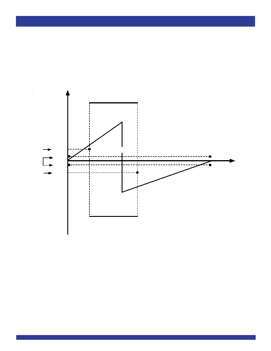
V-I CHARACTERISTICS OF BUS-HOLD CIRCUIT
V
T
Threshold Voltage
1.5V
V
IL
.8 V
IH
2V
ACTIVE TERMINATOR OR `BUS-HOLD' CIRCUIT
The Active Terminator circuit, also known as the Bus-hold circuit, is configured as a "weak latch" with positive feedback. When connected to a TTL
or CMOS input port, the Bus-hold circuit holds the last logic state at the input when the input is "disconnected" from the driver. When the output of a device
connected to such an input attempts a logic level transition, it will over-drive the Bus-hold circuit. The primary benefit of this circuit is that it prevents CMOS
inputs from floating, a situation which should be avoided to prevent spurious switching of inputs and unnecessary power dissipation. Bus-hold is a better
solution than the traditional approach of using resistive termination to V
CC
or GND to prevent bus floating, because the Bus-hold circuit does not consume
any static power.
The figure above shows the input V-I characteristics of a Bus-hold implementation. The input characteristics resemble a resistor. As the input voltage
is increased from 0 volts, the `sink' current increases linearly. When the TTL threshold of the circuit is reached (typically 1.5 volts), the latch changes the
logic state due to positive feedback and the direction of current is reversed. As the voltage is further increased towards V
CC
, the input `source' current
begins to decrease, reaching the lowest level at V
IN =
V
CC.
6
INDUSTRIAL TEMPERATURE RANGE
IDTQS3388
HIGH-SPEED CMOS BUS EXCHANGE SWITCH WITH ACTIVE TERMINATION
ORDERING INFORMATION
CORPORATE HEADQUARTERS
for SALES:
for Tech Support:
2975 Stender Way
800-345-7015 or 408-727-6116
logichelp@idt.com
Santa Clara, CA 95054
fax: 408-492-8674
(408) 654-6459
www.idt.com
IDTQS
XXXXX
XX
Package
Device Type
Blank
Industrial (-40∞C to +85∞C)
Quarter Size Outline Package
Q
3388
High Speed CMOS Bus Exchange Switch
with Active Termination (Bus Hold)
X
Process