 | –≠–ª–µ–∫—Ç—Ä–æ–Ω–Ω—ã–π –∫–æ–º–ø–æ–Ω–µ–Ω—Ç: IDTQS3389 | –°–∫–∞—á–∞—Ç—å:  PDF PDF  ZIP ZIP |
1
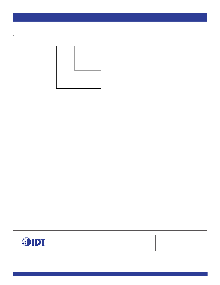
IDTQS3389
LAST VALUE LATCH 20 ACTIVE TERMINATORS (BUS HOLD)
COMMERCIAL TEMPERATURE RANGE
DECEMBER 1999
1999 Integrated Device Technology, Inc.
DSC-5733/1
c
COMMERCIAL TEMPERATURE RANGE
FEATURES:
∑ Active termination pulls bus pins to rails
∑ Holds last value of input signal
∑ Ideal replacement for resistive termination
∑ Ultra low 3
µµ
µµ
µA DC quiescent current
∑ Bus-hold eliminates floating bus lines and reduces static
power consumption
∑ Low power QCMOS technology
∑ Operates over 2.7V to 5.5V Vcc range
∑ TTL-compatible input and output levels
∑ No added noise or ground bounce
∑ 20 independent terminator circuits
∑ Available in QSOP package
The IDT logo is a registered trademark of Integrated Device Technology, Inc.
APPLICATIONS:
∑ Bus termination
∑ Extend data hold time
IDTQS3389
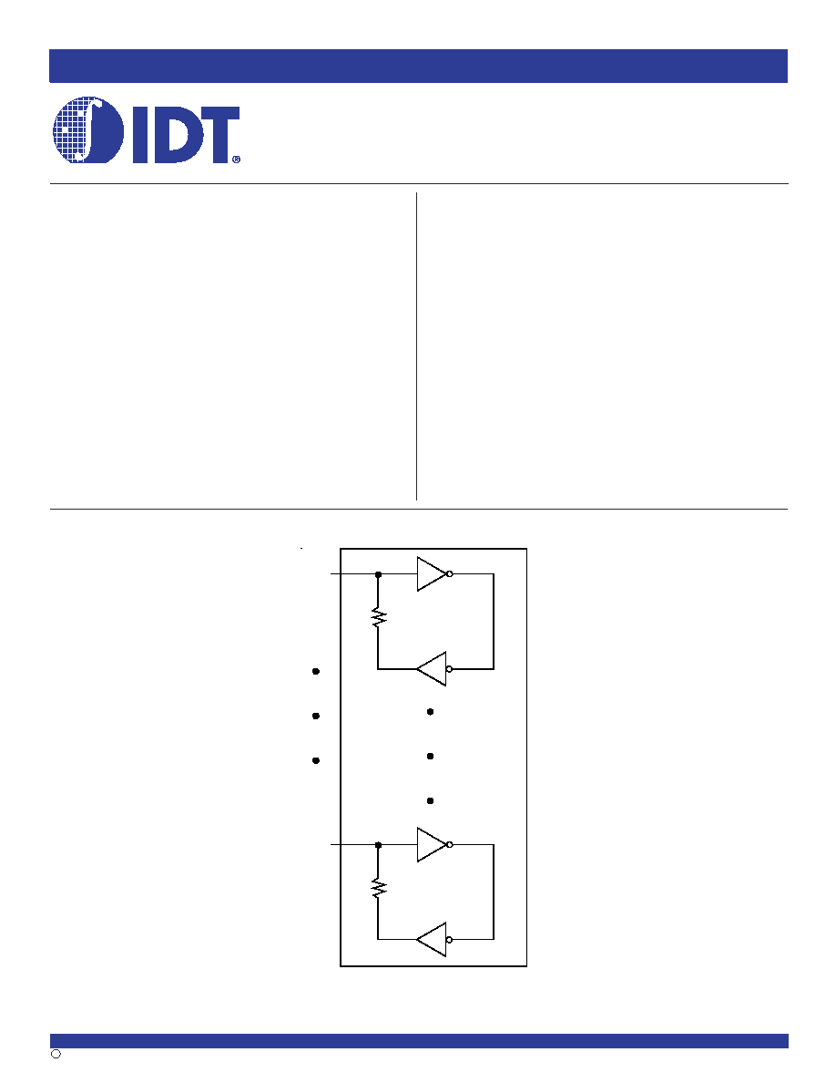
FUNCTIONAL BLOCK DIAGRAM
QUICKSWITCH
Æ
PRODUCTS
LAST VALUE LATCH
20 ACTIVE BUS TERMINATORS
(BUS HOLD)
DESCRIPTION:
The QS3389 provides a set of 20 active termination circuits which pull data
bus signals to the voltage rails. This feature prevents bus signals from floating
in the threshold region of standard TTL I/O devices. The QS3389 can
replace resistor termination solutions which add DC power dissipation and
increase component count. Input clamp diodes help to reduce reflections
and undershoot in transmission line environments. Importantly, the termi-
nator circuits pull signals to whichever logic state the signal previously held
(high or low). For this reason, this device is also referred to as a last value
latch. This device is appropriate for data bus applications where interfacing
devices have CMOS inputs with low input currents. These terminators
provide sufficient drive to overcome leakage currents and drive corre-
sponding signals away from the TTL threshold region.
The QS3389 is characterized for operation at 0∞C to +70∞C.
T
0
T
19
7K
7K
2
COMMERCIAL TEMPERATURE RANGE
IDTQS3389
LAST VALUE LATCH 20 ACTIVE TERMINATORS (BUS HOLD)
PIN CONFIGURATION
Symbol
Description
Max
Unit
V
TERM
(2)
Supply Voltage to Ground
≠0.5 to +7
V
V
TERM
(3)
DC Switch Voltage V
S
≠0.5 to +7
V
V
AC
AC Input Voltage (pulse width
20ns)
≠3
V
I
OUT
DC Output Current
120
mA
P
MAX
Maximum Power Dissipation (T
A
= 85∞C)
0.5
W
T
STG
Storage Temperature
≠65 to +150
∞C
ABSOLUTE MAXIMUM RATINGS
(1)
Pins
Typ.
Max.
(1)
Unit
T
19
- T
0
3
4
pF
CAPACITANCE
(T
A
= +25∞C, f = 1MHz, V
IN
= 0V, V
OUT
= 0V)
NOTE:
1. This parameter is guaranteed but not production tested.
NOTES:
1. Stresses greater than those listed under ABSOLUTE MAXIMUM RATINGS may cause
permanent damage to the device. This is a stress rating only and functional operation
of the device at these or any other conditions above those indicated in the operational
sections of this specification is not implied. Exposure to absolute maximum rating
conditions for extended periods may affect reliability.
2. V
CC
terminals.
3. All terminals except V
CC
.
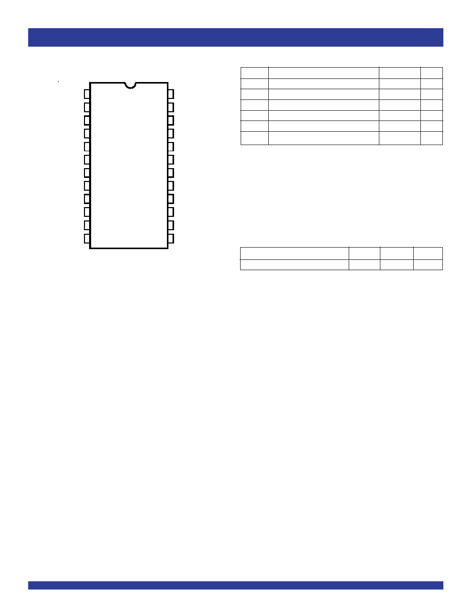
QSOP
TOP VIEW
24
23
22
21
20
19
18
17
16
15
14
13
T
0
T
1
T
2
T
3
T
4
T
5
T
6
T
7
T
8
T
9
GND
V
CC
T
10
T
11
T
12
T
13
T
14
T
15
T
16
T
17
T
18
T
19
GND
1
2
3
4
5
6
7
8
9
10
11
12
V
CC
3
IDTQS3389
LAST VALUE LATCH 20 ACTIVE TERMINATORS (BUS HOLD)
COMMERCIAL TEMPERATURE RANGE
Symbol
Parameter
Test Conditions
Min.
Typ.
(1)
Max.
Unit
V
IH
Input HIGH Voltage
Guaranteed Logic HIGH for Control Pins
2
--
--
V
V
IL
Input LOW Voltage
Guaranteed Logic LOW for Control Pins
--
--
0.8
V
V
T
Threshold Voltage
--
1.5
--
V
I
IN
Input Leakage Current
(2)
V
IN
= Vcc or GND
--
--
±5
µA
I
BH
Input Current
(5)
Vcc = Max., V
IN
= 0V or Vcc
--
--
±20
µA
Input HIGH or LOW Bus Hold Inputs
(2,3)
Vcc = Max., 0.8V < V
IN
< 2V
--
--
±500
(4)
I
BHH
Bus Hold Sustaining Current
(6,7)
Vcc = Min., V
IN
= 2V
≠
60
--
--
µA
I
BHL
Bus Hold Inputs
Vcc = Min., V
IN
= 0.8V
+60
--
--
µA
R
T
Terminator Resistance
--
7k
--
DC ELECTRICAL CHARACTERISTICS OVER OPERATING RANGE
Following Conditions Apply Unless Otherwise Specified:
Commercial: T
A
= 0∞C to +70∞C, V
CC
= 5V ± 5%
NOTE:
1. For conditions shown as Min. or Max., use the appropriate values specified under DC Electrical Characteristics.
POWER SUPPLY CHARACTERISTICS
Symbol
Parameter
Test Conditions
(1)
Max.
Unit
I
CCQ
Quiescent Power Supply Current
V
CC
= Max., V
IN
= GND or V
CC
, f = 0
1.5
mA
NOTES:
1. Typical values are at V
CC
= 5.0V, T
A
= 25∞C.
2. Trip current definition (see Functional Block Diagram):
An external driver must source at least I
TL
to switch the node from LOW to HIGH.
An external driver must sink at least I
TH
to switch the node from HIGH to LOW.
3. Hold current definition (see Functional Block Diagram):
I
HH
is the Maximum Curent the QS3389 can sink without raising the node above V
IL
max.
I
HL
is the Maximum Curent the QS3389 can source without lowering the node below V
IH
min.
4. An external driver must provide at least I
BH
during transition to guarantee that the Bus-Hold input will change states.
5. I
BH
is the magnitude of the input current specified under two conditions:
a) Input voltage at GND or Vcc. This indicates the input current under steady-state condition.
b) Input voltage between 0.8V and 2V (TTL input threshold range). This indicates the maximum input current during transient condition. The driver connected to the
input must overcome this current requirement in order to switch the logic state of the bus-hold circuit.
6. I
BHL
is the minimum sustaining "sink" current at the input for V
IN
= 0.8V. This parameter signifies the latching capability of the bus-hold circuit in logic LOW state.
7. I
BHH
is the minimum sustaining "source" current at the input for V
IN
= 2V. This parameter signifies the latching capability of the bus-hold circuit in logic HIGH state.
4
COMMERCIAL TEMPERATURE RANGE
IDTQS3389
LAST VALUE LATCH 20 ACTIVE TERMINATORS (BUS HOLD)
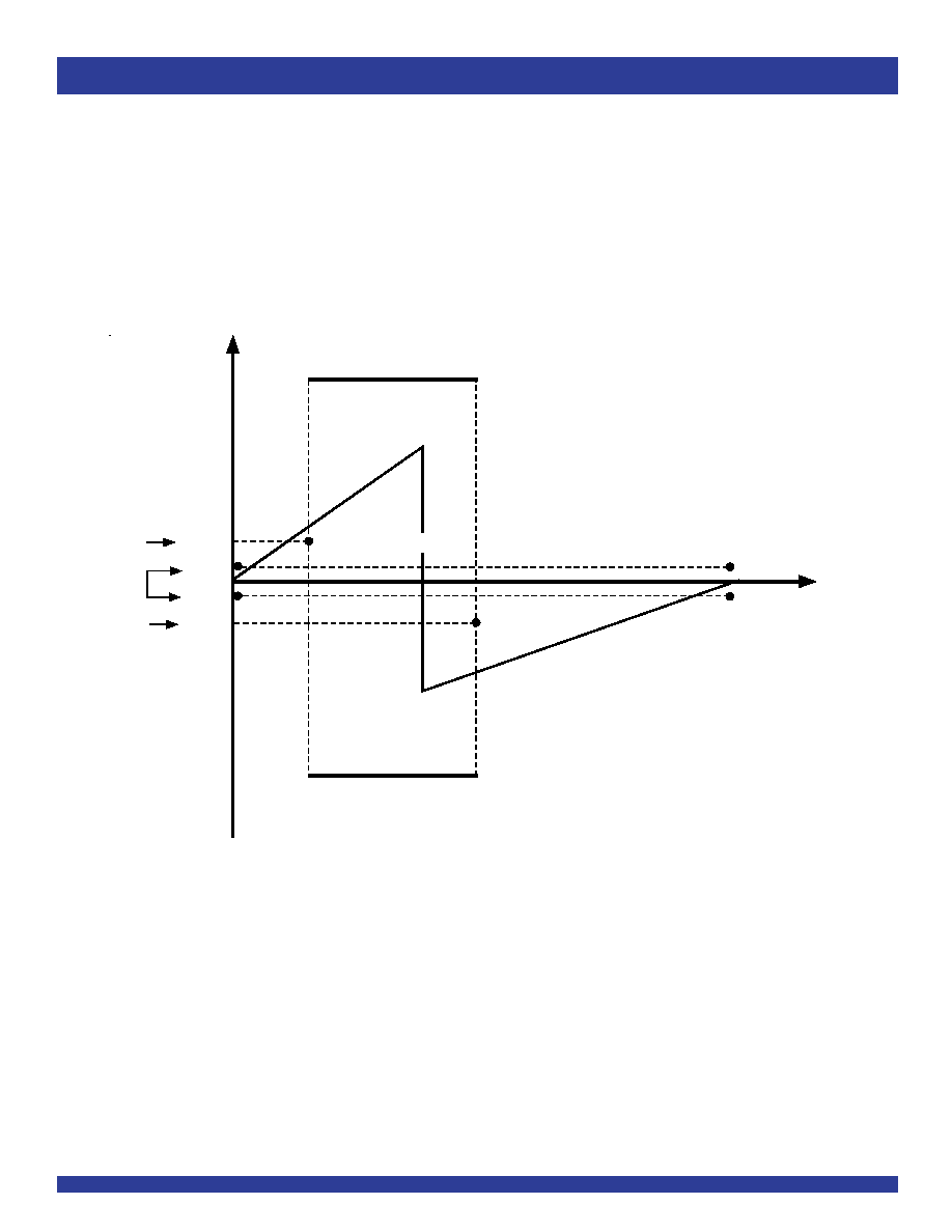
V-I CHARACTERISTICS OF BUS-HOLD CIRCUIT
ACTIVE TERMINATOR OR `BUS-HOLD' CIRCUIT
The Active Terminator circuit, also known as the Bus-hold circuit, is configured as a "weak latch" with positive feedback. When connected to a TTL
or CMOS input port, the Bus-hold circuit holds the last logic state at the input when the input is "disconnected" from the driver. When the output of a device
connected to such an input attempts a logic level transition, it will over-drive the Bus-hold circuit. The primary benefit of this circuit is that it prevents CMOS
inputs from floating, a situation which should be avoided to prevent spurious switching of inputs and unnecessary power dissipation. Bus-hold is a better
solution than the traditional approach of using resistive termination to V
CC
or GND to prevent bus floating, because the Bus-hold circuit does not consume
any static power.
The figure above shows the input V-I characteristics of a Bus-hold implementation. The input characteristics resemble a resistor. As the input voltage
is increased from 0 volts, the `sink' current increases linearly. When the TTL threshold of the circuit is reached (typically 1.5 volts), the latch changes the
logic state due to positive feedback and the direction of current is reversed. As the voltage is further increased towards V
CC
, the input `source' current
begins to decrease, reaching the lowest level at V
IN =
V
CC.
I
BH
+500
Sinking
Current
( + )
I
BHL
I
BH
I
BHH
+60
+20
≠ 60
≠ 20
+60
I
BHL
0.8V
2V
V
IH
≠ 60 I
BHH
V
IL
Sourcing
Current
( ≠ )
I
BH
≠ 500
Vcc
+20 I
BH
≠ 20 I
BH
Voltage
V
T
V
T
Threshold Voltage
1.5V
V
IL
.8 V
IH
2V
5
IDTQS3389
LAST VALUE LATCH 20 ACTIVE TERMINATORS (BUS HOLD)
COMMERCIAL TEMPERATURE RANGE
ORDERING INFORMATION
CORPORATE HEADQUARTERS
for SALES:
for Tech Support:
2975 Stender Way
800-345-7015 or 408-727-6116
logichelp@idt.com
Santa Clara, CA 95054
fax: 408-492-8674
(408) 654-6459
www.idt.com
IDTQS
XXXXX
XX
Package
Device Type
Blank
Commercial (0∞C to +70∞C)
Quarter Size Outline Package
Q
3389
Last Value Latch 20 Active Terminators (Bus Hold)
X
Process