1
IDTQS33X253
HIGH-SPEED CMOS QUICKSWITCH MULTIWIDTH 24:6 MUX/DEMUX
INDUSTRIALTEMPERATURE RANGE
JANUARY 2000
1999 Integrated Device Technology, Inc.
DSC-5761/-
c
IDTQS33X253
INDUSTRIAL TEMPERATURE RANGE
QUICKSWITCH
Æ
PRODUCTS
HIGH-SPEED CMOS
QUICKSWITCH MULTIWIDTH
24:6 MUX/DEMUX
DESCRIPTION:
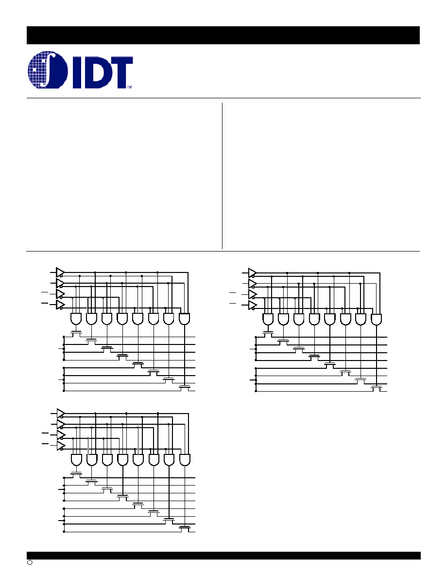
The QS33X253 is a high-speed CMOS 24:6 (3, dual 4:1) multiplexer/
demultiplexer. The QS33X253 is a member of the MultiWidthTM family and
is functionally compatible to three of the QuickSwitch version of the 74F253,
74FCT253, and the 74ALS/AS/LS253 Dual 4:1 multiplexers. The low ON
resistance of the QS33X253 allows inputs to be connected to outputs without
adding propagation delay and without generating additional ground bounce
noise. TTL-compatible control circuitry with "Break-before-make" feature
avoids bus contention on the demux side. This part is ideal for video
switching and four way memory bank interleaving applications.
Mux/Demux devices provide an order of magnitude faster speed than
equivalent logic devices.
The QS33X253 is characterized for operation at -40∞C to +85∞C.
S0
EF
Y
E
I0
E
I1
E
I2
E
I3
E
I0
F
I1
F
I2
F
I3
F
Y
F
S1
EF
E E
E F
S0
AB
Y
A
I0
A
I1
A
I2
A
I3
A
I0
B
I1
B
I2
B
I3
B
Y
B
S1
AB
E A
E B
S0
CD
Y
C
I0
C
I1
C
I2
C
I3
C
I0
D
I1
D
I2
D
I3
D
Y
D
S1
CD
EC
ED
FUNCTIONAL BLOCK DIAGRAM
FEATURES:
-
Enhanced N channel FET with no inherent diode to Vcc
-
Bidirectional switches connect inputs to outputs
-
24:6 Mux/Demux switches
-
Zero propagation delay, zero ground bounce
-
Individual controls for each bank
-
Undershoot clamp diodes on all switch and control pins
-
TTL-compatible control inputs
-
Available in 48-pin QVSOP Package
APPLICATIONS
-
Logic replacment
-
Video, audio, graphics switching, muxing
-
Hot-swapping, hot-docking
-
Voltage translation (5V to 3.3V)
2
INDUSTRIALTEMPERATURE RANGE
IDTQS33X253
HIGH-SPEED CMOS QUICKSWITCH MULTIWIDTH 24:6 MUX/DEMUX
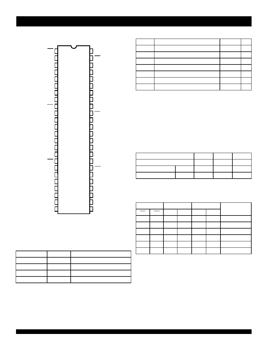
1
2
3
4
5
6
7
8
9
10
11
12
13
14
15
16
17
18
19
20
21
22
23
24
48
47
46
45
44
43
42
41
40
39
38
37
36
35
34
33
32
31
30
29
28
27
26
25
EA
V
C C
I
3 A
I
2 A
I
1 A
I
0 A
Y
A
G ND
S1
AB
EC
G ND
S1
CD
EE
G ND
S1
EF
EB
V
C C
S0
AB
ED
V
C C
S0
CD
EF
S0
EF
I
3 C
I
2 C
I
1 C
I
0 C
Y
C
I
3 E
I
2 E
I
1 E
I
0 E
Y
E
I
3 B
I
2 B
I
1 B
I
0 B
Y
B
I
3 D
I
2 D
I
1 D
I
0 D
Y
D
I
3F
I
2F
I
1F
I
0F
Y
F
PIN CONFIGURATION
QVSOP
TOP VIEW
PIN DESCRIPTION
Pin Names
I/O
Description
Ixx
I
Data Inputs
S
0
xx, S
1
xx
I
Select Inputs
Ex
I
Enable Inputs
Yx
O
Data Outputs
ABSOLUTE MAXIMUM RATINGS
(1)
Symbol
Description
Max.
Unit
V
TERM(2)
Supply Voltage to Ground
≠ 0.5 to +7
V
V
TERM(3)
DC Switch Voltage V
S
≠ 0.5 to +7
V
V
TERM(3)
DC Input Voltage V
IN
≠ 0.5 to +7
V
V
AC
AC Input Voltage (pulse width
20ns)
-3
V
I
OUT
DC Output Current
120
mA
P
MAX
Maximum Power Dissipation (T
A
= 85
∞
C)
.5
W
T
STG
Storage Temperature
≠ 65 to +150
∞C
NOTES:
1. Stresses greater than those listed under ABSOLUTE MAXIMUM
RATINGS may cause permanent damage to the device. This is a
stress rating only and functional operation of the device at these or
any other conditions above those indicated in the operational sections
of this specification is not implied. Exposure to absolute maximum
rating conditions for extended periods may affect reliability.
2. Vcc Terminals.
3. All terminals except Vcc.
CAPACITANCE
(T
A
= +25
O
C, f = 1.0MHz, V
IN
= 0V, V
OUT
= 0V)
Pins
Typ.
Max.
(1)
Unit
Control Inputs
4
5
pF
Quickswitch Channels
Demux
5
7
pF
(Switch OFF)
Mux
14
16
pF
NOTE:
1. This parameter is guaranteed at characterization but not tested.
FUNCTION TABLE
(1, 2)
Enable
Select
Outputs
EA
EB
S
1AB
S
0AB
Y
A
Y
B
Function
H
X
X
X
Hi-Z
X
Disable A
X
H
X
X
X
Hi-Z
Disable B
L
L
L
L
I
0A
I
0B
S
1
- 0 = 0
L
L
L
H
I
1A
I
1B
S
1
- 0 = 1
L
L
H
L
I
2A
I
2B
S
1
- 0 = 2
L
L
H
H
I
3A
I
3B
S
1
- 0 = 3
NOTES:
1. H = HIGH Voltage Level
L = LOW Voltage Level
X = Don't Care
Z = High-Impedence
2. This table represents the function for block "AB".
The "CD" block nomenclature substitutes "A" for "C" and "B" for "D".
The "EF" block nomenclature substitutes "A" for "E" and "B" for "F".
3
IDTQS33X253
HIGH-SPEED CMOS QUICKSWITCH MULTIWIDTH 24:6 MUX/DEMUX
INDUSTRIALTEMPERATURE RANGE
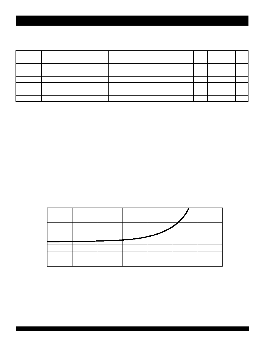
TYPICAL ON RESISTANCE vs V
IN
AT V
CC
= 5V
R
ON
(ohms)
V
IN
(Volts)
16
14
12
10
8
6
4
2
0
0.0
0.5
1.0
1.5
2.0
2.5
3.0
3.5
DC ELECTRICAL CHARACTERISTICS OVER OPERATING RANGE
Following Conditions Apply Unless Otherwise Specified:
Industrial: T
A
= -40∞C to +85∞C, V
CC
= 5.0V ± 5%
Symbol
Parameter
Test Conditions
Min.
Typ.
(1)
Max.
Unit
V
IH
Input HIGH Voltage
Guaranteed Logic HIGH for Control Inputs
2
--
--
V
V
IL
Input LOW Voltage
Guaranteed Logic LOW for Control Inputs
--
--
0.8
V
I
IN
Input Leakage Current (Control Inputs)
0V
V
IN
Vcc
--
--
±1
µ
A
I
OZ
Off-State Current (Hi-Z)
0V
V
OUT
Vcc
--
--
±1
µ
A
R
ON
Switch ON Resistance
Vcc = Min., V
IN
= 0V
,
I
ON
= 30mA
--
7
10
R
ON
Switch ON Resistance
Vcc = Min., V
IN
= 2.4V
,
I
ON
= 15mA
--
10
15
V
P
Pass Voltage
(2)
V
IN
= Vcc = 5V, I
OUT
= -5
µ
A
3.7
4
4.2
V
NOTES:
1. Typical values are at V
CC
= 5.0V, T
A
= 25∞C.
2. Pass voltage is guaranteed but not production tested.
4
INDUSTRIALTEMPERATURE RANGE
IDTQS33X253
HIGH-SPEED CMOS QUICKSWITCH MULTIWIDTH 24:6 MUX/DEMUX
POWER SUPPLY CHARACTERISTICS
Symbol
Parameter
Test Conditions
(1)
Max.
Unit
I
CCQ
Quiescent Power Supply Current
V
CC
= Max., V
IN
= GND or Vcc, f = 0
9
µ
A
I
CC
Power Supply Current per Control Input HIGH
(2)
V
CC
= Max., V
IN
= 3.4V , f = 0
1.5
mA
I
CCD
Dynamic Power Supply Current per MHz
(3)
V
CC
= Max., I and Y pins open
Control Input Toggling at 50% Duty Cycle
0.25
mA/MHz
NOTES:
1. For conditions shown as Min. or Max., use the appropriate values specified under DC Electrical Characteristics.
2. Per TTL driven input (V
IN
= 3.4V, control inputs only). I and Y pins do not contribute to
Icc
.
3. This current applies to the control inputs only and represents the current required to switch internal capacitance at the specified frequency. The I
and Y inputs generate no significant AC or DC currents as they transition. This parameter is guaranteed but not production tested.
SWITCHING CHARACTERISTICS OVER OPERATING RANGE
T
A
= -40∞C to +85∞C, V
CC
= 5.0V ± 5%
C
LOAD
= 50pF, R
LOAD
= 500
unless otherwise noted.
Symbol
Parameter
Min.
(1)
Typ.
Max.
Unit
t
PLH
t
PHL
Data Propagation Delay
(2, 3)
In to Y
--
--
0.25
ns
t
PZL
t
PZH
Switch Turn-On Delay
Sn to Y
0.5
--
6.6
ns
t
PZL
t
PZH
Switch Turn-Off Delay
En to Y
0.5
--
6
ns
t
PLZ
t
PHZ
Switch Turn-Off Delay
(2)
En to Y, Sn to Y
0.5
--
6
ns
NOTES:
1. Minimums guaranteed but not tested.
2. This parameter is guaranteed but not tested
3. The bus switch contributes no propagation delay other than the RC delay of the ON resistance of the switch and the load capacitance. The time
constant for the switch alone is of the order of 0.25ns for C
L
= 50pF. Since this time constant is much smaller than the rise and fall times of typical
driving signals, it adds very little propagation delay to the system. Propagation delay of the bus switch, when used in a system, is determined by the
driving circuit on the driving side of the switch and its interaction with the load on the driven side.
5
IDTQS33X253
HIGH-SPEED CMOS QUICKSWITCH MULTIWIDTH 24:6 MUX/DEMUX
INDUSTRIALTEMPERATURE RANGE
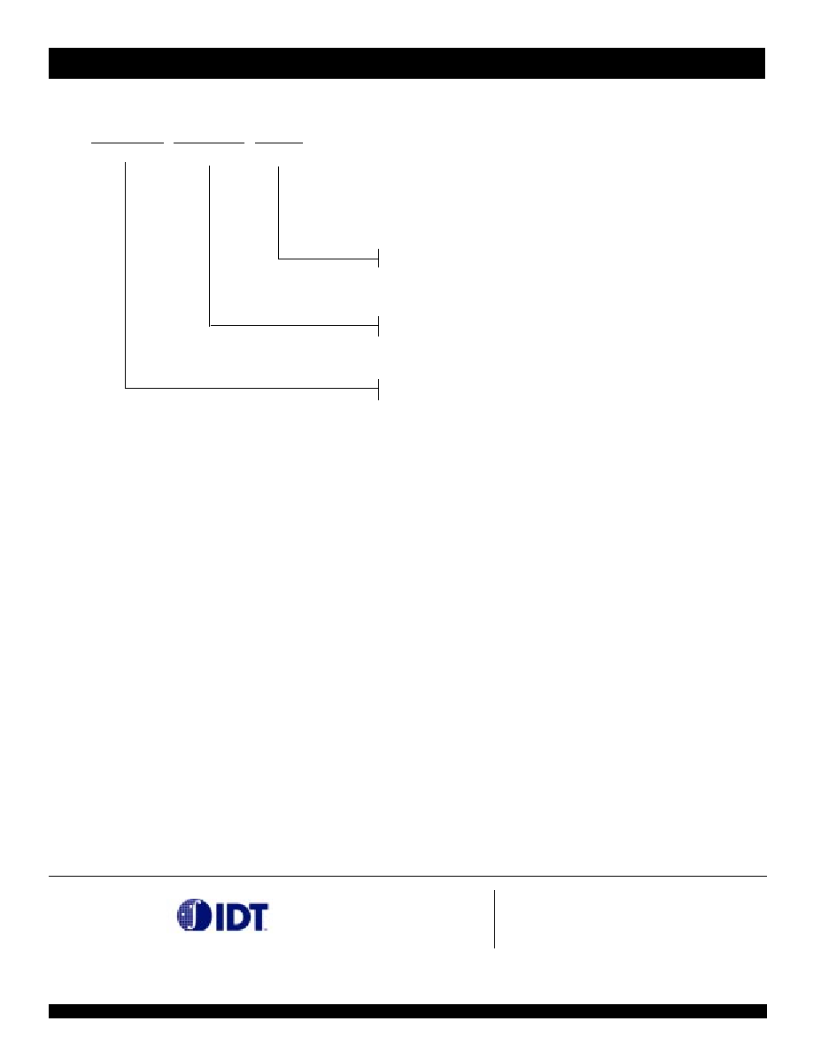
IDTQS
XXXXX
XX
Package
Device Type
Blank
Industrial (-40∞C to +85∞C)
QVSOP
Q1
33X253
High Speed CMOS Quickswitch Multiwidth 24:6
Mux/Demux
X
Process
ORDERING INFORMATION
CORPORATE HEADQUARTERS
for SALES:
2975 Stender Way
800-345-7015 or 408-727-6116
Santa Clara, CA 95054
fax: 408-492-8674
www.idt.com*
*To search for sales office near you, please click the sales button found on our home page or dial the 800# above and press 2.
The IDT logo, QuickSwitch, and SynchroSwitch are registered trademarks of Integrated Device Technology, Inc.