 | –≠–ª–µ–∫—Ç—Ä–æ–Ω–Ω—ã–π –∫–æ–º–ø–æ–Ω–µ–Ω—Ç: IDTQS3862 | –°–∫–∞—á–∞—Ç—å:  PDF PDF  ZIP ZIP |
1
IDTQS3862
HIGH-SPEED CMOS 10-BIT BUS SWITCH WITH ACTIVE ENABLES
INDUSTRIAL TEMPERATURE RANGE
FEBRUARY 2000
1999 Integrated Device Technology, Inc.
DSC-5734/-
c
IDTQS3862
INDUSTRIAL TEMPERATURE RANGE
QUICKSWITCH
Æ
PRODUCTS
HIGH-SPEED CMOS 10-BIT
BUS SWITCH WITH ACTIVE
HIGH AND LOW ENABLES
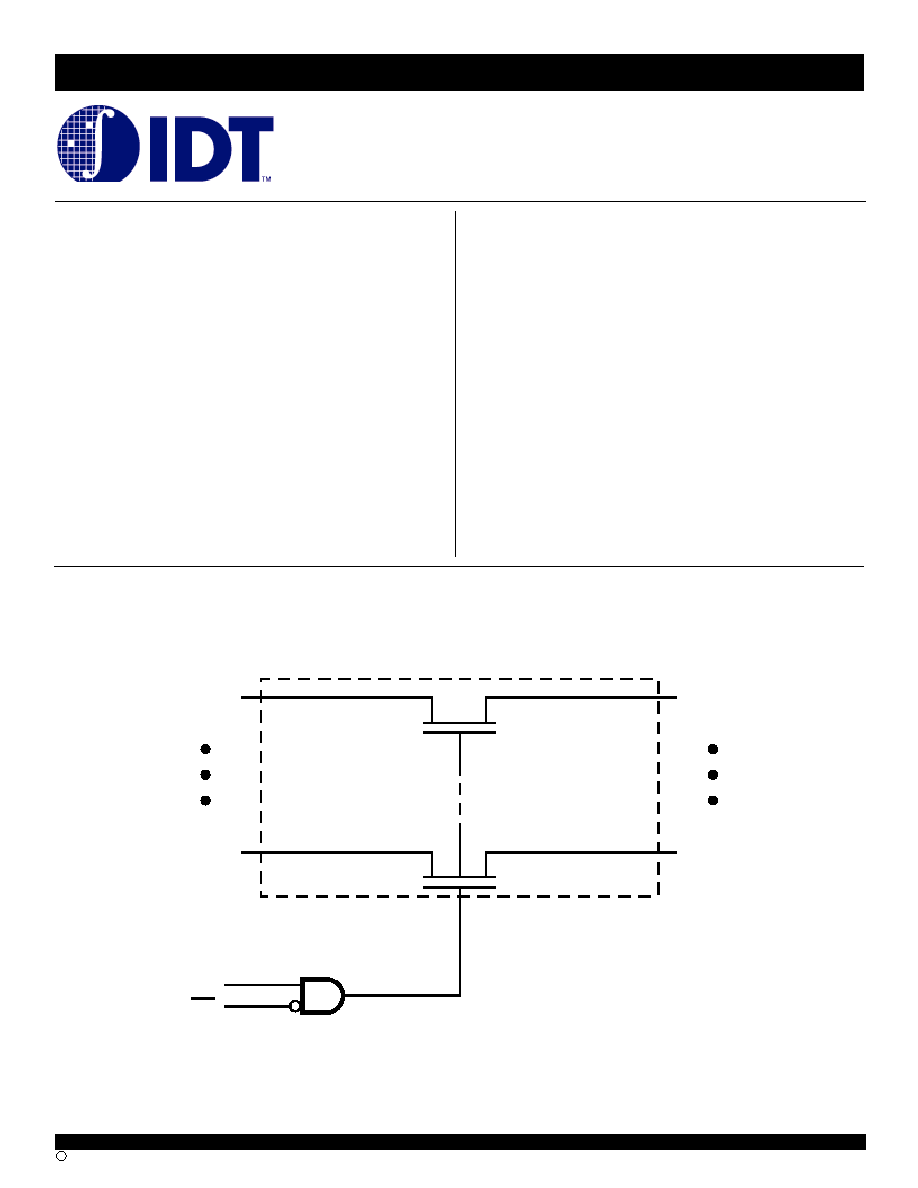
DESCRIPTION:
The QS3862 provides a set of ten high speed CMOS, TTL Compatible
bus switches. The low ON resistance (5
) of the QS3862 allows inputs to
be connected to outputs without adding propagation delay and without
generating additional ground bounce noise. The switches are controlled by
independent active Low enable (
BE) and active High enable (BE) controls.
The QS3862 is ideal for switching digital buses as well as hot-plugging,
hot-docking, and voltage translation.
The QS3862 is characterized for operation at -40∞C to +85∞C.
A
0
A
9
B
0
B
9
BE
BE
FUNCTIONAL BLOCK DIAGRAM
FEATURES:
-
Enhanced N channel FET with no inherent diode to Vcc
-
5
bidirectional switches connect inputs to outputs
-
Zero propagation delay, zero ground bounce
-
Undershoot clamp diodes on all switch and control inputs
-
Active low and high enable control
-
Available in SOIC and QSOP packages
APPLICATIONS
-
Hot-swapping, hot-docking
-
Voltage translation (5V to 3.3V)
-
Power conservation
-
Capacitance reduction and isolation
-
Applications requiring Active-High enabling
-
Clock gating
-
Bus isolation
2
INDUSTRIAL TEMPERATURE RANGE
IDTQS3862
HIGH-SPEED CMOS 10-BIT BUS SWITCH WITH ACTIVE ENABLES
PIN CONFIGURATION
24
23
22
21
20
19
18
17
16
15
14
13
BE
A
0
A
1
A
2
A
3
A
4
A
5
A
6
A
7
A
8
A
9
G ND
V
C C
B
0
B
1
B
2
B
3
B
4
B
5
B
6
B
7
B
8
B
9
1
2
3
4
5
6
7
8
9
10
11
12
BE
SO24-2
SO24-8
SOIC/ QSOP
TOP VIEW
ABSOLUTE MAXIMUM RATINGS
(1)
Symbol
Description
Max.
Unit
V
TERM(2)
Supply Voltage to Ground
≠ 0.5 to +7
V
V
TERM(3)
DC Switch Voltage V
S
≠ 0.5 to +7
V
V
TERM(3)
DC Input Voltage V
IN
≠ 0.5 to +7
V
V
AC
AC Input Voltage (pulse width
20ns)
-3
V
I
OUT
DC Output Current
120
mA
P
MAX
Maximum Power Dissipation
0.5
W
T
STG
Storage Temperature
≠ 65 to +150
∞C
NOTES:
1. Stresses greater than those listed under ABSOLUTE MAXIMUM
RATINGS may cause permanent damage to the device. This is a
stress rating only and functional operation of the device at these or
any other conditions above those indicated in the operational sections
of this specification is not implied. Exposure to absolute maximum
rating conditions for extended periods may affect reliability.
2. Vcc Terminals.
3. All terminals except Vcc.
CAPACITANCE
(T
A
= +25
O
C, f = 1.0MHz, V
IN
= 0V, V
OUT
= 0V)
Pins
Typ.
Max.
(1)
Unit
Control Inputs
3
5
pF
Quickswitch Channels (Switch OFF)
5
7
pF
NOTE:
1. This parameter is guaranteed but not production tested.
PIN DESCRIPTION
Pin Names
I/O
Description
BE
I
Active High Bus Enable
BE
I
Active High Bus Enable
A
0
≠ A
9
I/O
Bus A
B
0
≠ B
9
I/O
Bus B
FUNCTION TABLE
(1)
BE
BE
A
0
≠ A
9
Function
L
L
Hi-Z
Disconnect
L
H
Hi-Z
Disconnect
H
L
B
0
≠ B
9
Connect
H
H
Hi-Z
Disconnect
NOTE:
1. H = HIGH Voltage Level
L = LOW Voltage Level
Z = High-impedence
3
IDTQS3862
HIGH-SPEED CMOS 10-BIT BUS SWITCH WITH ACTIVE ENABLES
INDUSTRIAL TEMPERATURE RANGE
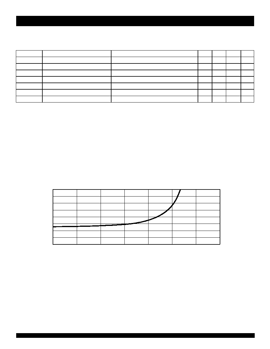
R
ON
(ohms)
V
IN
(Volts)
TYPICAL ON RESISTANCE vs V
IN
AT V
CC
= 5V
16
14
12
10
8
6
4
2
0
0.0
0.5
1.0
1.5
2.0
2.5
3.0
3.5
DC ELECTRICAL CHARACTERISTICS OVER OPERATING RANGE
Following Conditions Apply Unless Otherwise Specified:
Industrial: T
A
= -40∞C to +85∞C, V
CC
= 5.0V ± 10%
Symbol
Parameter
Test Conditions
Min.
Typ.
(1)
Max.
Unit
V
IH
Input HIGH Voltage
Guaranteed Logic HIGH for Control Pins
2
--
--
V
V
IL
Input LOW Voltage
Guaranteed Logic LOW for Control Pins
--
--
0.8
V
I
IN
Input Leakage Current (Control Inputs)
0V
V
IN
Vcc
--
±0.01
±1
µ
A
I
OZ
Off-State Current (Hi-Z)
0V
V
OUT
Vcc, Switches OFF
--
±0.01
±1
µ
A
R
ON
Switch ON Resistance
Vcc = Min., V
IN
= 0V
,
I
ON
= 30mA
--
5
7
R
ON
Switch ON Resistance
Vcc = Min., V
IN
= 2.4V
,
I
ON
= 15mA
--
10
15
V
P
Pass Voltage
(2)
V
IN
= V
CC
= 5V, I
OUT
= -5
µ
A
3.7
4
4.2
V
NOTES:
1. Typical values are at V
CC
= 5.0V, T
A
= 25∞C.
2. Pass voltage is guaranteed but not production tested.
4
INDUSTRIAL TEMPERATURE RANGE
IDTQS3862
HIGH-SPEED CMOS 10-BIT BUS SWITCH WITH ACTIVE ENABLES
POWER SUPPLY CHARACTERISTICS
Symbol
Parameter
Test Conditions
(1)
Typ.
(2)
Max.
Unit
I
CCQ
Quiescent Power Supply Current
V
CC
= Max., V
IN
= GND or Vcc, f = 0
0.2
3
µ
A
I
CC
Power Supply Current per Control Input HIGH
V
CC
= Max., V
IN
= 3.4V
(3)
, f = 0
--
2.5
mA
I
CCD
Dynamic Power Supply Current per MHz
(4)
V
CC
= Max., A and B pins open,
BE,
BE inputs
Toggling at 50% Duty Cycle
--
0.25
mA/MHz
NOTES:
1. For conditions shown as Min. or Max., use the appropriate values specified under DC Electrical Characteristics.
2. Typical values are at V
CC
= 5.0V, T
A
= 25∞C ambient.
3. Per TLL driven input (V
IN
= 3.4V, control inputs only). A and B pins do not contribute to
Icc
.
4. This current applies to the control inputs only and represents the current required to switch internal capacitance at the specified frequency. The A
and B inputs generate no significant AC or DC currents as they transition. This parameter is guaranteed but not production tested.
SWITCHING CHARACTERISTICS OVER OPERATING RANGE
T
A
= -40∞C to +85∞C, V
CC
= 5.0V ± 10%
C
LOAD
= 50pF, R
LOAD
= 500
unless otherwise noted.
Symbol
Parameter
Min.
(1)
Typ.
Max.
Unit
t
PLH
t
PHL
Data Propagation Delay
(2,3)
A to B or B to A
--
--
0.25
ns
t
PZL
t
PZH
Switch Turn-on Delay
BE or BE to A to B
1.5
--
6.5
ns
t
PLZ
t
PHZ
Switch Turn-off Delay
(2)
BE or BE to A to B
1.5
--
5.5
ns
NOTES:
1. Minimums are guaranteed but not production tested.
2. This parameter is guaranteed but not production tested.
3. The time constant for the switch alone is of the order of 0.25ns for C
L
= 50pF. The bus switch contributes no propagation delay other than the RC
delay of the ON resistance of the switch and the load capacitance. Since this time constant is much smaller than the rise and fall times of typical
driving signals, it adds very little propagation delay to the system. Propagation delay of the bus switch, when used in a system, is determined by the
driving circuit on the driving side of the switch and its interaction with the load on the driven side.
5
IDTQS3862
HIGH-SPEED CMOS 10-BIT BUS SWITCH WITH ACTIVE ENABLES
INDUSTRIAL TEMPERATURE RANGE
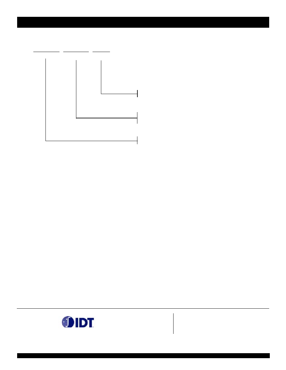
ORDERING INFORMATION
IDTQ S
X XX XX
X X
P ackage
Device Type
B lank
Industrial (-40∞C to +85∞C )
S m all O utline IC (S O 24-2)
Quarter-S ize O utline P ackage (S O24-8)
S O
Q
3862
High S peed CM OS 10-B it Bus S witch with
A ctive H igh and Low E nables
X
P rocess
CORPORATE HEADQUARTERS
for SALES:
2975 Stender Way
800-345-7015 or 408-727-6116
Santa Clara, CA 95054
fax: 408-492-8674
www.idt.com*
*To search for sales office near you, please click the sales button found on our home page or dial the 800# above and press 2.
The IDT logo, QuickSwitch, and SynchroSwitch are registered trademarks of Integrated Device Technology, Inc.