 | –≠–ª–µ–∫—Ç—Ä–æ–Ω–Ω—ã–π –∫–æ–º–ø–æ–Ω–µ–Ω—Ç: NW6003 | –°–∫–∞—á–∞—Ç—å:  PDF PDF  ZIP ZIP |

TYPE II CALLER ID DECODER
NW6003
The IDT logo is a registered trademark of Integrated Device Technology, Inc
INDUSTRIAL TEMPERATURE RANGE
JULY 2002
©
2002 Integrated Device Technology, Inc.
DSC-6047/2
FEATURES
∑
1200 baud Bell 202 and ITU-T V.23 Frequency Shift Keying (FSK)
Demodulation
∑
Compliant with three specifications:
Bellcore GR-30-CORE & SR-TSV-002476
British Telecom (BT) SIN227 & SIN242
Cable Communication Association (CCA) TW/P&E/312
∑
Bellcore "CPE Alerting Signal (CAS)" and British Telecom "Idle
State and Loop State Tone Alert Signal" detection
∑
Ring and line reversal detection
∑
High sensitivity with -40 dBV input Tone and FSK Detection
∑
Serial data interface to microcontroller
∑
3 V ±10% or 5 V ±10% operation
∑
Low power CMOS with powerdown mode
∑
Operating temperature range: -40 ∞C to +85 ∞C
∑
Packages available:
NW6003-XS 24 pin SOIC
(where `X' is the revision ID)
Figure 1. Block Diagram
Oscillator
Line Reverse
and
Ring Detector
3 V/5 V
Detector
Bias
Generator
Interrupt
Generator
Guard Time
Dual Tone
Detector
FSK
Demodulator
Data/Timing Recovery
+
-
TRIGIN
TRIGRC
TRIGOUT
OSCIN
OSCOUT
VREF
CAP
PWDN
IN +
IN -
GS
FSKEN
MODE
DR
DATA
DCLK
CD
EST
ST/GT
STD
INT
DESCRIPTION
The NW6003 device is a single-chip, 3/5 Volt CMOS caller ID and
call waiting detection circuit. It can receive signals following Bellcore
GR-30-CORE & SR-TSV-002476, BT SIN227 & SIN242, and CCA TW/
P&E/312 specifications.
The NW6003 provides 1200 baud Bell 202 and ITU-T V.23 FSK
demodulation. It allows a microcontroller to extract data from it via a
serial interface. In addition, the NW6003 offers Idle State and Loop
State Tone Alert Signal and line reversal detection capability for BT
CLIP, ring burst detection for the CCA CLIP, and ring and CAS
detection for Bellcore CID.
The device can be used in feature or cordless phones for BT
Calling Line Identity Presentation (CLIP), CCA CLIP and Bellcore
Calling Identity Delivery (CID) systems. It can also be used in caller ID
boxes, modem, fax machines, answering machines, database query
systems and Computer Telephony Integration (CTI) systems.
FUNCTIONAL BLOCK DIAGRAM

2
INDUSTRIAL TEMPERATURE RANGE
NW6003 TYPE II CALLER ID DECODER
PIN INFORMATION
Figure 2. Pin Assignment
IN+
IN-
GS
VREF
CAP
TRIGIN
TRIGRC
TRIGOUT
MODE
OSCIN
OSCOUT
GND
VCC
ST/GT
EST
STD
INT
CD
DR
DATA
DCLK
FSKEN
PWDN
TM
24
23
22
21
20
19
18
17
16
15
14
13
1
2
3
4
5
6
7
8
9
10
11
12
Name
Type Pin No.
Description
IN+
I
1
Non-inverting Input of the gain adjustable op amp.
IN-
I
2
Inverting Input of the gain adjustable op amp.
GS
O
3
Gain Select Output of the gain adjustable op amp.
Select the op amp gain by adjusting the resistor ratio in the feed-back resistor network.
VREF
O
4
Reference Voltage.
This output is used to bias the input op amp. It is typically VCC/2.
CAP
O
5
Capacitor Connector.
A 0.1
µ
F decoupling capacitor should be connected between this pin and GND.
TRIGIN
I
6
Trigger Input.
This is a Schmitt trigger input used for ring detection and line reversal detection.
TRIGRC
I/O
7
Trigger Resistor and Capacitor Connector.
This pin is connected to VCC and GND through resistor and capacitor. The RC value
decides the time delay from TRIGIN going inactive (low) to TRIGOUT becoming inactive
(high). See Fig.6 for reference.
TRIGOUT
O
8
Trigger Output.
This is a Schmitt trigger buffer output indicating the detection of line reversal and/or ringing.
MODE
I
9
Serial FSK Interface MODE Select.
A low level on this pin sets the interface to mode '0', while a high level sets it to mode '1'.
OSCIN
I
10
Oscillator Input.
A 3.579545 MHz crystal or ceramic resonator should be connected between this pin and
the OSCOUT. It can also be driven by an external clock source.
OSCOUT
O
11
Oscillator Output.
A 3.579545 MHz crystal or ceramic resonator should be connected between this pin and
and OSCIN. When OSCIN is driven by an external clock, this pin should be left floating.
GND
--
12
Ground.
TM
I
13
Test Mode. Must be connected to GND for normal operation.

3
INDUSTRIAL TEMPERATURE RANGE
NW6003 TYPE II CALLER ID DECODER
Abbreviation Index
CAS ----------------------------------------------------------- CPE Alerting Signal
CDS ----------------------------------------------------------- Caller Display Service
CID ------------------------------------------------------------ Calling Identity Delivery
CIDCW ------------------------------------------------------- Calling Identity Delivery on Call Waiting
CLIP ---------------------------------------------------------- Calling Line Identity Presentation
CNAM -------------------------------------------------------- Calling Name Delivery
CND ---------------------------------------------------------- Calling Number Delivery
CNIC --------------------------------------------------------- Calling Number Identification Circuit
CO ------------------------------------------------------------- Central Office
CTI ----------------------------------------------------------- Computer Telephony Integration
TE -------------------------------------------------------------- Terminal Equipment
PIN INFORMATION (CONTINUED)
Name
Type Pin No.
Description
PWDN
I
14
Power Down.
This is an active high Schmitt trigger input. When active, the device enters a minimal
power state by disabling all internal functional circuits except TRIGIN, TRIGRC and TRIGOUT.
It must be low for normal operation.
FSKEN
I
15
FSK Enable.
When this pin is high, FSK demodulation is enabled. This pin should be set low to disable
the FSK demodulator from reacting to extraneous signals such as speech, alert signal etc.
DCLK
I/NC
16
Data Clock.
In mode '0' (MODE pin low), this pin is unused. In mode '1' (MODE pin high), this pin is an
input, Data Clock is provided by microcontroller.
DATA
O
17
Data Output.
In mode '0', data appears on this pin once demodulated. In mode '1', data is shifted out on the
rising edge of DCLK, which is supplied by microcontroller.
DR
O/NC
18
Data Ready Output.
In mode '0', this pin is unused. In mode '1', this pin indicates to the microcontroller that 8-bit
data is ready. Microcontroller initializes the DCLK signal to read out the data.
CD
O
19
FSK Carrier Detect .
This is an active low CMOS output signal to indicate the presence of in-band FSK signal.
INT
OD
20
Interrupt.
This is an active low open drain output. This pin is used to interrupt the microcontroller when
TRIGOUT or DR is low, or STD is high. It remains low until all three signals become inactive.
STD
O
21
Dual Tone Alert Signal Delayed Steering Output.
An active high signal to indicate the detection of a "guard time qualified" Dual Tone Alert Signal.
EST
O
22
Dual Tone Alert Signal Early Steering Output.
This pin is an active high output to indicate the detection of Dual Tone Alert Signal.
ST/GT
I/O
23
Dual Tone Alert Signal Steering Input/Guard Time.
It's a CMOS output and an input of voltage comparator. If the voltage at this pin is greater than
voltage threshold (See Fig-6), STD is asserted high to indicate that a dual tone has been
detected. A voltage less than threshold enables the device to accept a new dual tone. External
RC are connected to EST and VCC pins.
VCC
--
24
3/5 V Power Supply.
4
INDUSTRIAL TEMPERATURE RANGE
NW6003 TYPE II CALLER ID DECODER
FUNCTIONAL DESCRIPTION
CALLER ID SPECS SUPPORTED
The NW6003 is a type II Caller ID device with Call Waiting
capability. It supports Bellcore, BT and CCA specifications. The major
differences between above specs are as follows (refer to Figure 13,
Figure 14, Figure 15, Figure 16 and Figure 17):
BELLCORE
Bellcore GR-30-CORE and SR-TSV-002476 define the
requirement for the signaling services of Calling Number Delivery
(CND), Calling Name Delivery (CNAM) and Calling Identity Delivery
on Call Waiting (CIDCW).
In CND or CNAM service, information of the calling party is
embedded in the silent interval between the first and second ringings.
The NW6003 can detect the first ringing and then demodulate the
incoming Bell-202 FSK data. In CIDCW service, information about an
incoming caller is sent to the subscriber who is engaged in another
call. A CPE Alerting Signal (CAS) indicates that a CIDCW data is
incoming. The NW6003 can detect the alerting signal and demodulate
the incoming FSK information which contains CIDCW data. The
demodulated data is output onto the serial interface.
BRITISH TELECOM
BT SIN227 and SIN242 define the signal interface between the
Central Office (CO) and the Terminal Equipment (TE) for the Caller
Display Service (CDS). CDS provides CLIP (Calling Line Identity
Presentation) that delivers to an idle state (on hook) TE the identity of
an incoming caller before the first ring.
A polarity reversal on the A and B wires (see Figure 6) indicates the
arrival of a CDS call. After that comes an Idle State Tone Alert Signal,
and then Caller ID FSK information transmitted in ITU-T V.23 format.
When the subscriber is engaged in a call, the arrival of information
about another incoming call is indicated by a Loop State Tone Alert
Signal. The NW6003 can detect the line reversal and tone alert
signal, it can also demodulate the incoming ITU-T V.23 FSK signals.
CABLE COMMUNICATION ASSOCIATION
The CCA caller identity specification TW/P&E/312 defines a
different CDS TE interface. In this specificaiton, data is transmitted
after a single burst of ringing rather than before the first ringing cycle,
as specified in the BT. The Idle State Tone Alert Signal is not required
in this case. The CCA specifies that data can be transmitted in either
Bell-202 or ITU-T V.23 format. The NW6003 can detect the ring burst,
and then demodulate either of the FSK format.
BLOCK DESCRIPTION
The NW6003 requires a 3.579545 MHz system clock and consists
of four major functional blocks: Analog Input Circuit, CLIP/CID Call
Arrival Detection, Dual Tone Alert Signal Dectection, and FSK
Demodulation.
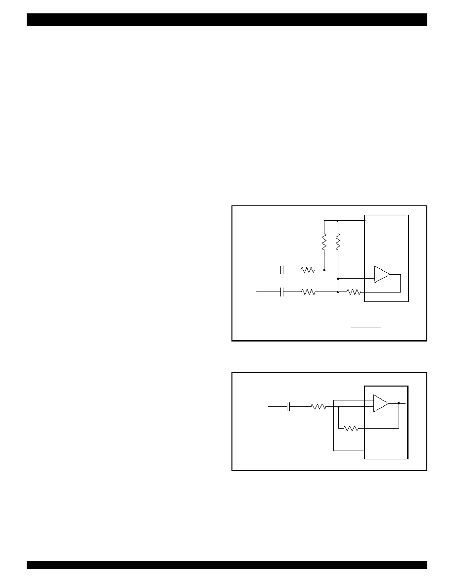
ANALOG INPUT CIRCUIT
The input signal is processed by the Analog Input Circuit block,
which is comprised of an operational amplifier and a bias source
(VREF). VREF is the output of a low impedance voltage source used
to bias the input op amp, and is typically equal to VCC/2. The gain
adjustable op amp is also used to select the input gain by connecting
a feedback resistor between GS and the IN- pin. Figure 3 shows the
necessary connections with the A/B line inputs. In single-ended
configuration, the gain adjustable op amp is connected as shown in
Figure 4.
R2
R1
R3
R4
R5
C1
C2
A
B
NW6003
V
REF
IN+
IN-
GS
Differential Input Amplifier
C1=C2
R1=R2 (For unity gain R5=R2)
R3=(R4R5)/(R4+R5)
Voltage Gain
Av = R5/R1
Input Impedance
Zin =2
R1
≤
+ (1/
C)≤
Figure 3. Differential Input Gain Control Circuit
Rin
Rf
C
Input
NW6003
IN+
IN-
GS
V
REF
Voltage Gain
Av = Rf / Rin
Figure 4. Single-ended Input Gain Control Circuit
5
INDUSTRIAL TEMPERATURE RANGE
NW6003 TYPE II CALLER ID DECODER
CLIP/CID CALL ARRIVAL DETECTION
Figure 6 shows the typical application circuit to detect the CLIP/CID
call arrival signals. The diode bridge works for both single ended and
balanced ring signals. R1 and R2 are used to set the maximum
loading and must be of some value to achieve balanced loading. The
ring signal is attenuated by R1, R3 and R4 resistor devider before
being applied to pin TRIGIN. The attenuation value is determined by
the detection of minimal ring voltage and maximum noise tolerance
between Ring/Tip and ground.
When no signal is applied to telephone line, TRIGIN will be at
ground and pin TRIGOUT will stay inactive high. If TRIGIN increases
from ground to VT+ (Schmitt trigger high going threshold voltage), C3
gets discharged, TRIGRC becomes low and TRIGOUT is asserted.
The low going TRIGOUT can be used to interrupt or wake up the
microcontroller. When TRIGIN signal drops below VT- (Schmitt trigger
low going threshold voltage), C3 will start to charge up through R5C3
time constant. After TRIGRC pin reaches above the threshhold voltage
(VT+), TRIGOUT becomes inactive high and it stops to interrupt the
microcontroller. To ensure the minimum TRIGOUT low interval and to
filter the ring signal to get a smooth envelope output, the RC time
constant should be greater than the maximum cycle time of the Ring
Signal.
Ring Detection for Bellcore: Bellcore recommends that the CID
FSK data be transmitted between first and second ringings. The circuit
in Figure 6 will generate a ring envelope signal at pin TRIGOUT for
the ring voltage of 40 Vrms or greater. R5 and C3 are used to filter the
ring signal to provide the envelope output.
Line Reversal Detection for BT: British Telecom uses the line
polarity reverse (+15 V to -15V between the two lines slewing in 30
ms) to indicate the arrival of an incoming CDS call. When line reverse
occurs, TRIGIN increases over VT+ and TRIGOUT signal becomes
active low. When reversal is over, TRIGIN falls below VT- and
TRIGOUT returns inactive high.
Ring Burst Detection for CCA: The CCA requires the TE to
detect a single burst of ringing followed by the FSK data. The ring
pulse may varies from 30 to 75 Vrms with pulse duration 200 - 450
ms.
R1 = 500K
R2 = 500K
R3 = 200K
R4 = 300K
R5 = 330K
C1= 0.1
µ
F
C2= 0.1
µ
F
N
C3 = 0.22
µ
F
Tip/A
Ring/B
TRIGIN
TRIGRC
TRIGOUT
NW6003
To Microcontroller
Note:
Minimal triggerable ring voltage (peak to
peak) is:
Vpp(max ring)=
2(VT+(max)(R1+R3+R4)/R4+0.7)
Tolerance to noise between Tip/Ring and Vss
is:
Vmax noise=
VT+(min)(R1+R3+R4)/R4+0.7
Suggested RC component value:
10K
< R5 < 500K
.
47 nF < C3 < 0.68
µ
F
Time constant is:
T=R5◊C3◊In(VCC/(VCC-VT+))
VT+(min) = 0.7 VCC
VT+(max) = 0.5 VCC
Figure 6. CLIP/CID Call Arrival Detection Circuit
Ring Signal
TRIGRC
TRIGOUT
TRIGIN
VT+
VT-
VT+
Figure 5. TRIGIN, TRIGRC and TRIGOUT Operation