TECHNICAL DATA
100mA ADJUSTABLE OUTPUT,
POSITIVE VOLTAGE REGULATOR IC
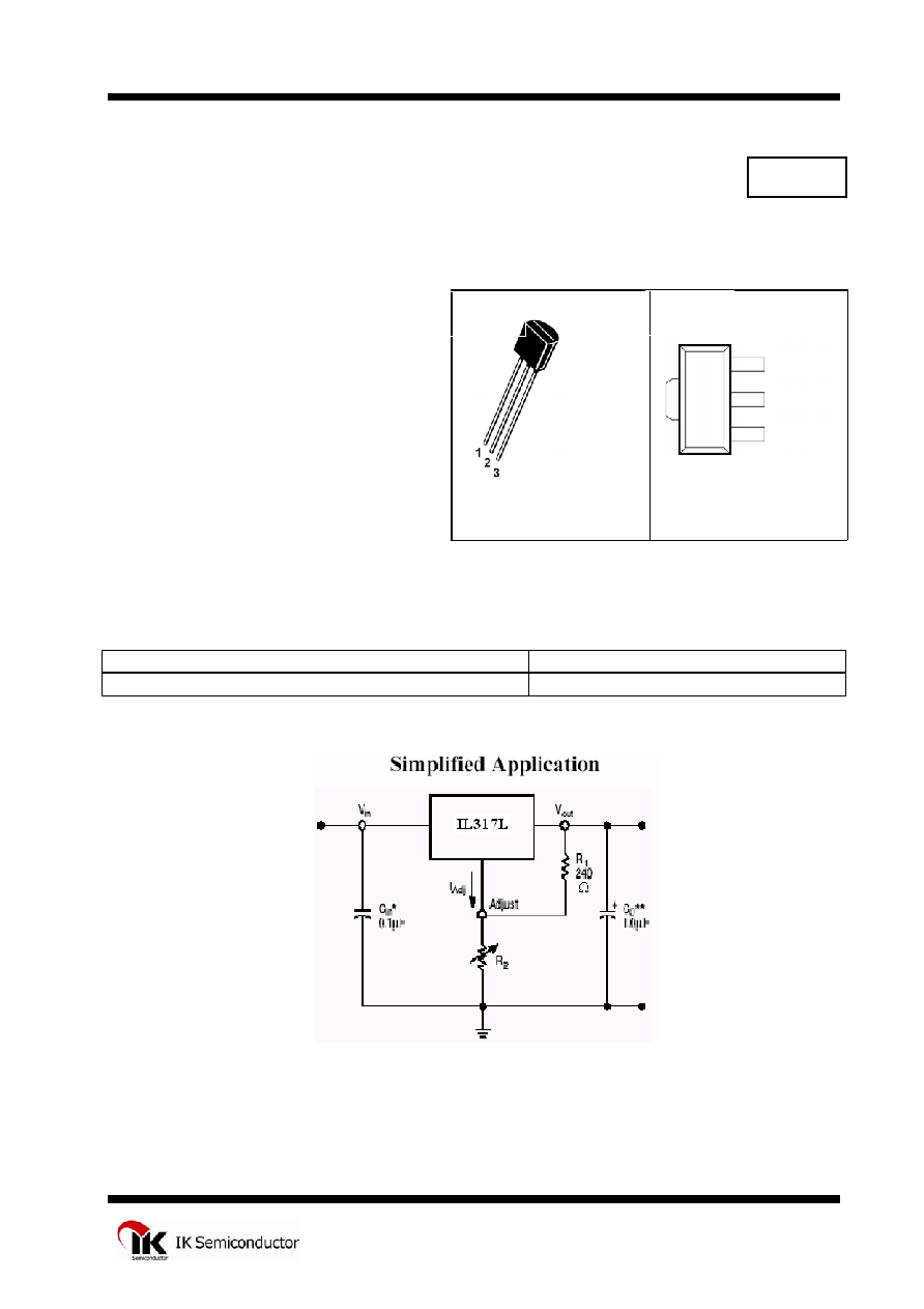
PIN CONNECTIONS
Features
∑
Output Current in Excess of 100mA
∑
Output Adjustable Between 1.2 V and
37 V
∑
Internal Shot Circuit Current Limiting
∑
Internal Thermal Overload Protection
∑
Output Transistor Safe-Area
Compensation
∑
Floating Operation for High Voltage
Applications
∑
Standard 3-Lead Transistor Package
∑
Eliminates Stocking Many Fixed Voltages
3. ADJUST
2. OUTPUT
1. INPUT
ADJUST
OUTPUT
INPUT
IL317L
SOT-89
TO-92
ABSOLUTE MAXIMUM RATINGS
Input - Output Voltage Differential
40 V
Operating Junction Temperature Range
-10
∞C to +125∞C
from power supply filter.
**Co is not needed for stability, however, it does improve transient response.
Vout = 1.25 V (1+R2/R1) + I
Adj
R2
Since I
Adj
is controlled to less than 100µA, the error associated with this term is
negligible in most applications.
1
IL317L
ELECTRICAL CHARACTERISTICS DIE ON WAFER
(VI - Vo = 3.0V, IO = 40mA, TA=25
∞C, unless otherwise noted, Imax and Pmax (Note 1)
CHARACTERISTIC
Symbol
TEST CONDITION
Min
Max
Unit
Reference Voltage
(TA= -10
∞C to +125∞C)
VO
3.0V
VI-Vo 40V
10mA
Io Imax, PD Pmax
1.2 1.3 V
Line Regulation (Note 2)
VOV 3.0V VI-Vo 40V, Io=10mA
160
mV
Line Regulation (TA= -10
∞C to
+125
∞C), (Note 2)
VOV 3.0V VI-Vo 40V, Io=10mA
180
mV
. Load Regulation, (Note 2)
VOI 10mA Io Imax, VO = 5.0V
6.0
mV
Load Regulation (TA= -10
∞C to
+125
∞C), (Note 2)
VOI 10mA Io Imax, VO = 5.0V
10
mV
Adjustment Pin Current
IAdj
10
100
µA
Adjustment Pin Current Change
IAdj 3.0V VI-Vo 40V
10mA
Io Imax, PD Pmax
5.0
µA
Maximum Output Current
IO MAX
VI-VO =3.0V, PD
Pmax
VI-VO = 40V, PD
Pmax
0.1
0.025
0.3
0.15
A
Minimum Load Current to Maintain
Regulation VO=1.2V, f=120Hz
IL MIN
VI-Vo
40V
10
mA
Ripple Rejection
RR
Vo = 1.2V, f= 120Hz
66
dB
Notes: 1. Imax=100mA, Pmax=625mW;
2. Load and line regulation are specified at constant junction temperature. Changes in VO due to heating
effects must be taken into account separately. Pulse testing with low duty cycle is used.
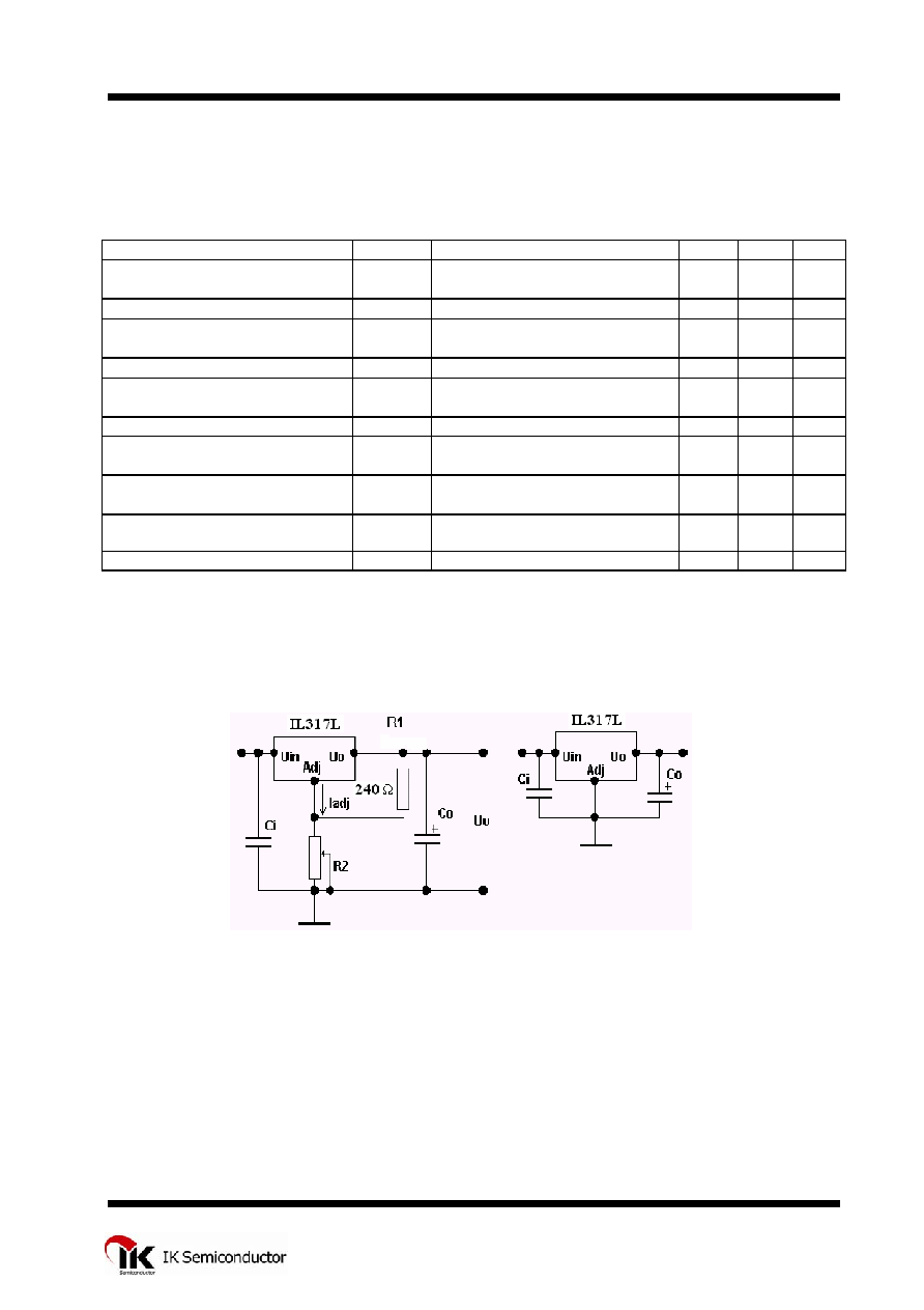
Fig.1 Test Circuit for Vo
>1.25V Fig.2 Test Circuit for Vo=1.25V
i=0,1
µF, o=1,0 µF. i=0,1µF, o=1,0 µF.
Vo=1,25(1+R2/R1)I
ADJ
R2
2