 | –≠–ª–µ–∫—Ç—Ä–æ–Ω–Ω—ã–π –∫–æ–º–ø–æ–Ω–µ–Ω—Ç: IW4034BN | –°–∫–∞—á–∞—Ç—å:  PDF PDF  ZIP ZIP |
TECHNICAL DATA
76
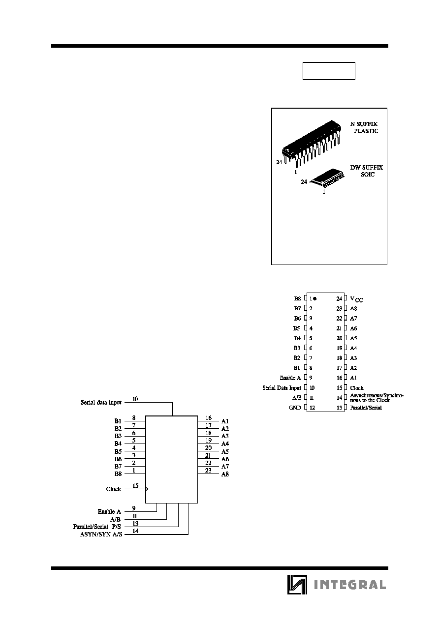
8-Stage Static Bidirectional Parallel/
Serial Input/Output Bus Register
High-Voltage Silicon-Gate CMOS
The IW4034B is a static eight-stage parallel-or serial-input
parallel-output register. It can be used to:
1) bidirectionally transfer parallel information between two buses,
2) convert serial data to parallel form and direct the parallel data to
either of two buses, 3) store (recirculate) parallel data, or 4) accept
parallel data from either of two buses and convert that data to serial
form. Inputs that control the operations include a single-phase CLOCK
(CL), A DATA ENABLE (AE),
ASYNCHRONOUS/SYNCHRONOUS (A/S), A-BUS-TO-B-BUS/ B-
BUS-TO-A-BUS (A/B), and PARALLEL/SERIAL (P/S).
Data inputs include 16 bidirectional parallel data lines of which the
eight A data lines are inputs (3-state outputs) and the B data lines are
outputs (inputs) dependung on the signal level on the A/B input. In
addition, an input for SERIAL DATA is also provided.
All register stages are D-type master-slave flip-flops with separate master and slave clock inputs generated
internally to allow synchronous or asynchronous data transfer from
master to slave.
∑
Operating Voltage Range: 3.0 to 18 V
∑
Maximum input current of 1
µ
A at 18 V over full package-
temperature range; 100 nA at 18 V and 25
∞
C
∑
Noise margin (over full package temperature range):
1.0 V min @ 5.0 V supply
2.0 V min @ 10.0 V supply
2.5 V min @ 15.0 V supply
IW4034B
ORDERING INFORMATION
IW4034BN Plastic
IW4034BDW SOIC
T
A
= -55
∞
to 125
∞
C for all packages
PIN ASSIGNMENT
LOGIC DIAGRAM
PIN 24=V
CC
PIN 12= GND
IW4034B
77
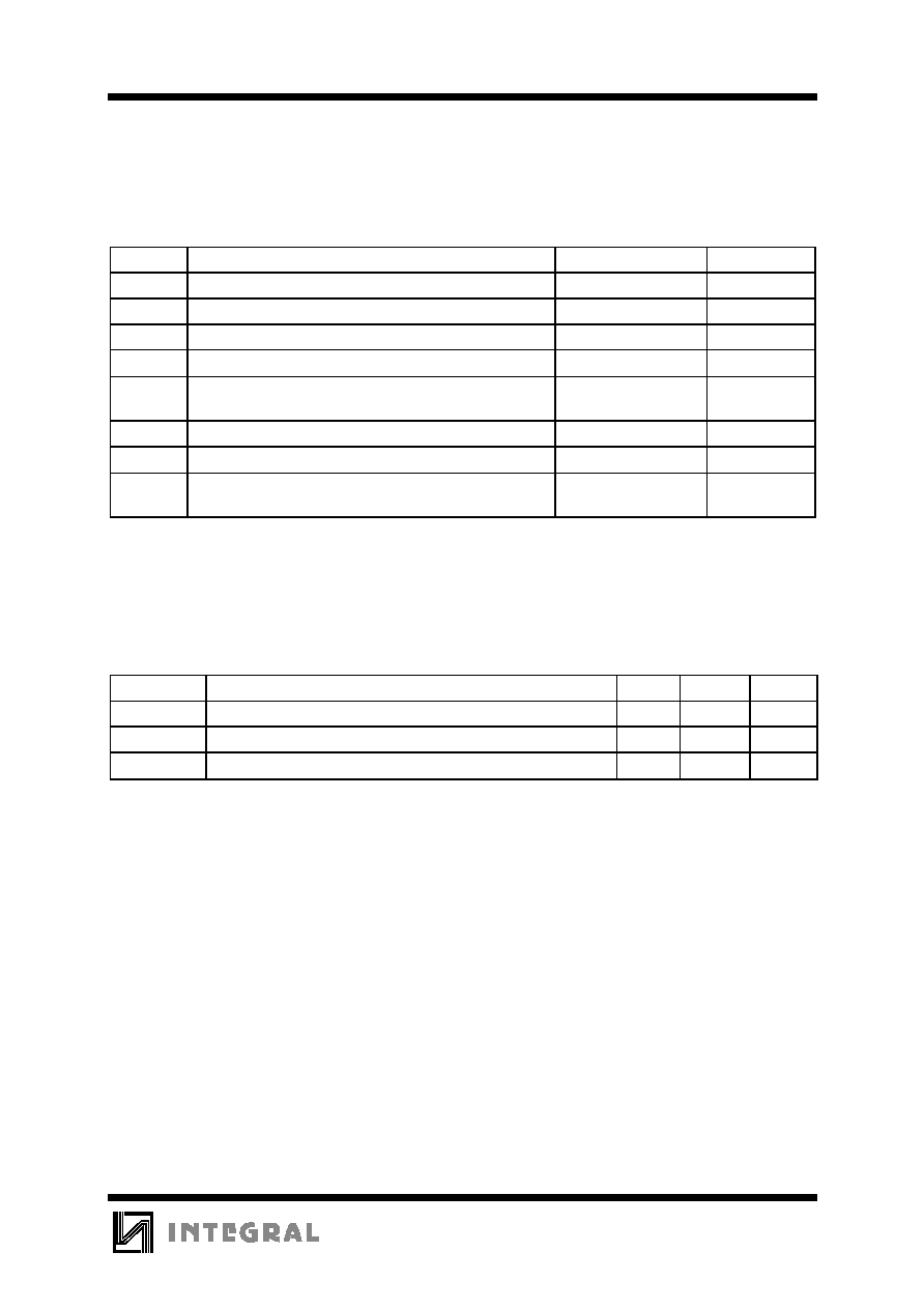
MAXIMUM RATINGS
*
Symbol
Parameter
Value
Unit
V
CC
DC Supply Voltage (Referenced to GND)
-0.5 to +20
V
V
IN
DC Input Voltage (Referenced to GND)
-0.5 to V
CC
+0.5
V
V
OUT
DC Output Voltage (Referenced to GND)
-0.5 to V
CC
+0.5
V
I
IN
DC Input Current, per Pin
±
10
mA
P
D
Power Dissipation in Still Air, Plastic DIP+
SOIC Package+
750
500
mW
P
D
Power Dissipation per Output Transistor
100
mW
Tstg
Storage Temperature
-65 to +150
∞
C
T
L
Lead Temperature, 1 mm from Case for 10 Seconds
(Plastic DIP or SOIC Package)
260
∞
C
*
Maximum Ratings are those values beyond which damage to the device may occur.
Functional operation should be restricted to the Recommended Operating Conditions.
+Derating - Plastic DIP: - 10 mW/
∞
C from 65
∞
to 125
∞
C
SOIC Package: : - 7 mW/
∞
C from 65
∞
to 125
∞
C
RECOMMENDED OPERATING CONDITIONS
Symbol
Parameter
Min
Max
Unit
V
CC
DC Supply Voltage (Referenced to GND)
3.0
18
V
V
IN
, V
OUT
DC Input Voltage, Output Voltage (Referenced to GND)
0
V
CC
V
T
A
Operating Temperature, All Package Types
-55
+125
∞
C
This device contains protection circuitry to guard against damage due to high static voltages or electric
fields. However, precautions must be taken to avoid applications of any voltage higher than maximum rated
voltages to this high-impedance circuit. For proper operation, V
IN
and V
OUT
should be constrained to the range
GND
(V
IN
or V
OUT
)
V
CC
.
Unused inputs must always be tied to an appropriate logic voltage level (e.g., either GND or V
CC
).
Unused outputs must be left open.
IW4034B
78
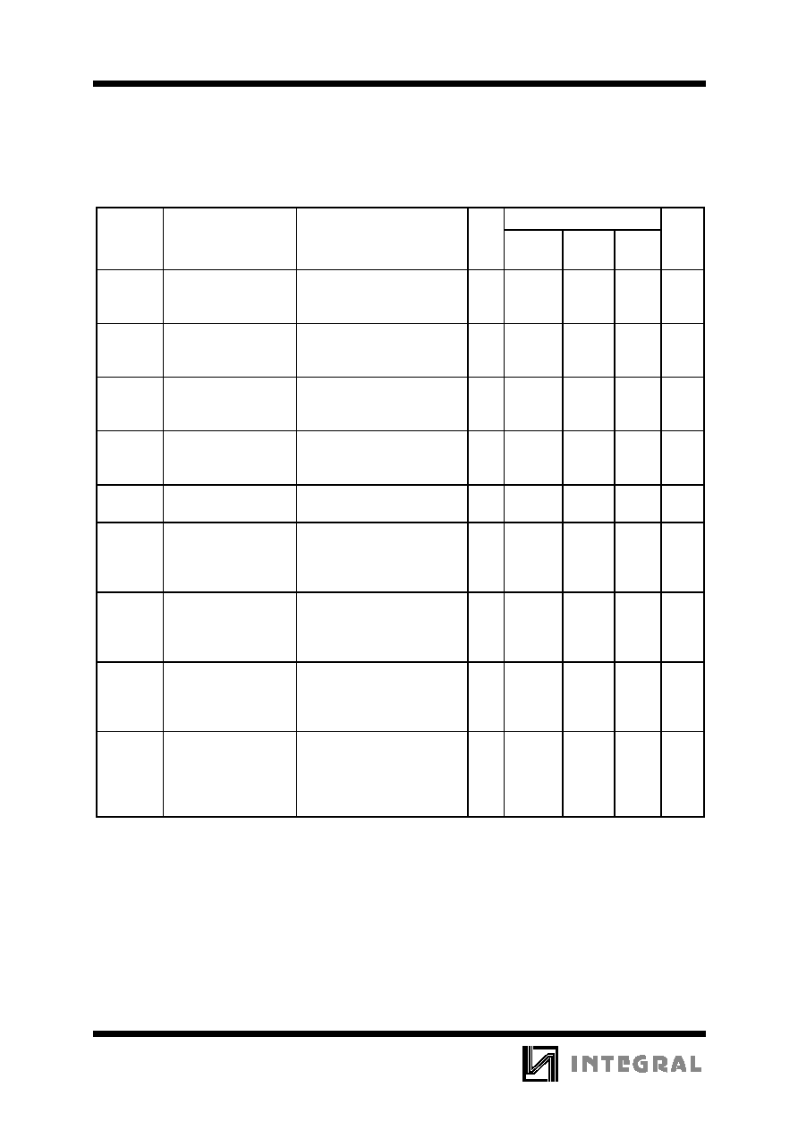
DC ELECTRICAL CHARACTERISTICS
(Voltages Referenced to GND)
V
CC
Guaranteed Limit
Symbol
Parameter
Test Conditions
V
-55
∞
C
25
∞
C
125
∞
C
Unit
V
IH
Minimum High-Level
Input Voltage
V
OUT
= 0.5 V or V
CC
- 0.5V
V
OUT
= 1.0 V or V
CC
- 1.0 V
V
OUT
= 1.5 V V
CC
- 1.5V
5.0
10
15
3.5
7
11
3.5
7
11
3.5
7
11
V
V
IL
Maximum Low -Level
Input Voltage
V
OUT
= 0.5 V or V
CC
- 0.5V
V
OUT
= 1.0 V or V
CC
- 1.0 V
V
OUT
= 1.5 V V
CC
- 1.5V
5.0
10
15
1.5
3
4
1.5
3
4
1.5
3
4
V
V
OH
Minimum High-Level
Output Voltage
V
IN
=GND or V
CC
5.0
10
15
4.95
9.95
14.95
4.95
9.95
14.95
4.95
9.95
14.95
V
V
OL
Maximum Low-Level
Output Voltage
V
IN
=GND or V
CC
5.0
10
15
0.05
0.05
0.05
0.05
0.05
0.05
0.05
0.05
0.05
V
I
IN
Maximum Input
Leakage Current
V
IN
= GND or V
CC
18
±
0.1
±
0.1
±
1.0
µ
A
I
OZ
Minimum Three State
Leakage Current
Output in High-Impedance
State
V
IN
= GND or V
CC
V
OUT
= GND or V
CC
18
±
0.4
±
0.4
±
12.0
µ
A
I
CC
Maximum Quiescent
Supply Current
(per Package)
V
IN
= GND or V
CC
5.0
10
15
20
5
10
20
100
5
10
20
100
150
300
600
3000
µ
A
I
OL
Minimum Output Low
(Sink) Current
V
IN
= GND or V
CC
U
OL
=0.4 V
U
OL
=0.5 V
U
OL
=1.5 V
5.0
10
15
0.64
1.6
4.2
0.51
1.3
3.4
0.36
0.9
2.4
mA
I
OH
Minimum Output
High (Source) Current
V
IN
= GND or V
CC
U
OH
=2.5 V
U
OH
=4.6 V
U
OH
=9.5 V
U
OH
=13.5 V
5.0
5.0
10
15
-2
-0.64
-1.6
-4.2
-1.6
-0.51
-1.3
-3.4
-1.15
-0.36
-0.9
-2.4
mA

IW4034B
79
AC ELECTRICAL CHARACTERISTICS
(C
L
=50pF, R
L
=200k
, Input t
r
=t
f
=20 ns)
V
CC
Guaranteed Limit
Symbol
Parameter
V
-55
∞
C
25
∞
C
125
∞
C
Unit
f
max
Maximum Clock Frequency (Figure 2)
5.0
10
15
2
5
7
2
5
7
1
2.5
3.5
MHz
t
PHL
, t
PLH
Maximum Propagation Delay, A(B) Parallel
Data In to B(A) Parallel Data Out; Serial to
Parallel Data Out (Figures 1,2)
5.0
10
15
700
240
170
700
240
170
1400
480
340
ns
t
PLZ
, t
PHZ,
t
PZL
, t
PZH
Maximum Propagation Delay, A/B or AE to
"A" Output (Figure 3)
5.0
10
15
400
160
120
400
160
120
800
320
240
ns
t
THL
, t
TLH
Maximum Output Transition Time, Any Output
(Figures 1,2)
5.0
10
15
200
100
80
200
100
80
400
200
160
ns
C
IN
Maximum Input Capacitance
-
7.5
pF
TIMING REQUIREMENTS
(C
L
=50pF, R
L
=200 k
, Input t
r
=t
f
=20 ns)
V
CC
Guaranteed Limit
Symbol
Parameter
V
-55
∞
C
25
∞
C
125
∞
C
Unit
t
su
Minimum Setup Time, Serial Data to Clock
(Figure 4)
5.0
10
15
160
60
40
160
60
40
320
120
80
ns
t
su
Minimum Setup Time, Parallel Data to Clock
(Figure 4)
5.0
10
15
50
30
20
50
30
20
100
60
40
ns
t
h
Minimum Hold Time, Clock to Data (Figure 4)
5.0
10
15
50
15
10
50
15
10
100
30
20
ns
t
w
Minimum Pulse Width, AE, P/S, A/S
(Figure 5)
5.0
10
15
350
140
80
350
140
80
700
280
160
ns
t
w
Minimum Pulse Width, Clock (Figure 2)
5.0
10
15
250
100
70
250
100
70
500
200
140
ns
t
r
,t
f
Minimum Input Rise or Fall Time, Clock
(Figure 2)
5.0
10
15
15
15
15
15
15
15
30
30
30
ns
IW4034B
80
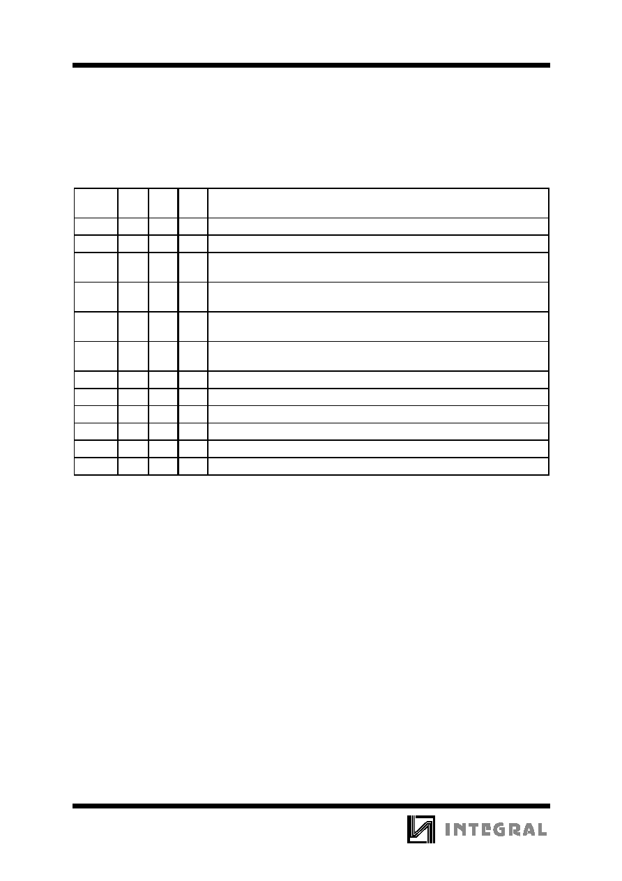
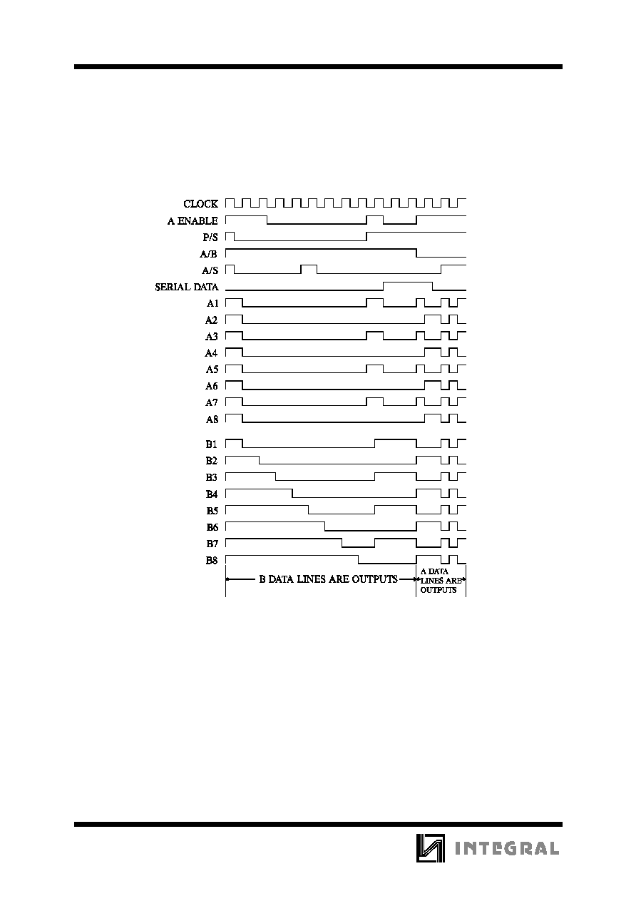
TRUTH TABLE FOR REGISTER INPUT-LEVELS AND RESULTING REGISTER
OPERATION
"A"
Enable
P/S
A/B
A/S
Operation
*
L
L
L
X
Serial Mode; Synch. Serial Data Input, "A" Parallel Data Outputs Disabled
L
L
H
X
Serial Mode, Synch. Serial Data Input, "B" Parallel Data Output
L
H
L
L
Parallel Mode; "B" Synch. Parallel Data Inputs, "A" Parallel Data Outputs
Disabled
L
H
L
H
Parallel Mode; "B" Asynch. Parallel Data Inputs, "A" Parallel Data Outputs
Disabled
L
H
H
L
Parallel Mode; "A" Parallel Data Inputs Disabled, "B" Parallel Data Outputs,
Synch. Data Recirculation
L
H
H
H
Parallel Mode; "A" Parallel Data Inputs Disabled, "B" Parallel Data Outputs,
Asynch. Data Recirculation
H
L
L
X
Serial Mode; Synch. Serial Data Input, "A" Parallel Data Output
H
L
H
X
Serial Mode; Synch. Serial Data Input, "B" Parallel Data Output
H
H
L
L
Parallel Mode; "B" Synch. Parallel Data Input, "A" Parallel Data Output
H
H
L
H
Parallel Mode; "B" Asynch. Parallel Data Input, "A" Parallel Data Output
H
H
H
L
Parallel Mode; "A" Synch. Parallel Data Input, "B" Parallel Data Output
H
H
H
H
Parallel Mode; "A" Asynch. Parallel Data Input, "B" Parallel Data Output
*
Outputs change at positive transition of clock in the serial mode and when the A/S control input is "low"
in the parallel mode. During transfer from parallel to serial operation A/S should remain low in oder to prevent
D
S
transfer into Flip Flops.
X = Don't Care
PARALLEL OPERATION
A high P/S input signal allows data transfer into the register via the parallel data lines synchronously with
the positive transition of the clock provided the A/S input is low. If the A/S input is high the transfer is
independent of the clock. The direction of data flow is controlled by the A/B input. When this signal is high the
A data lines are inputs (and B data lines are outputs); a low A/B signal reverses the direction of data flow.
The AE input is an additional feature which allows many registers to feed data to a common bus. The A
DATA lines are enabled only when this signal is high.
Data storage through recirculation of data in each register stage is accomplished by making the A/B signal
high and the AE signal low.
SERIAL OPERATION
A low P/S signal allows serial data to transfer into the register synchronously with the positive transition of
the clock. The A/S input is internally disabled when the register is in the serial mode (asynchronous serial
operation is not allowed).
The serial data appears as output data on either the B lines (when A/B is high) or the A lines (when A/B is
low and the AE signal is high).
IW4034B
81
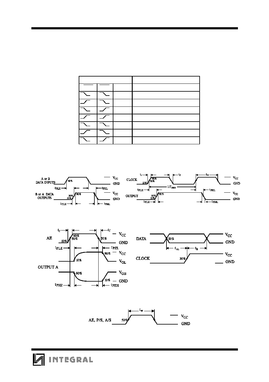
FLIP-FLOP TRUTH TABLE
Figure 1. Asynchronous operation
Figure 2. Synchronous operation
Figure 3. Switching Waveforms
Figure 4. Switching Waveforms
Figure 5. Switching Waveforms
Inputs
Output
CL
M
CL
S
D
Q
L
L
L
L
L
INVALID CONDITION
X
L
H
H
H
H
H
INVALID CONDITION
X = don't care
IW4034B
82
TIMING DIAGRAM
IW4034B
83
EXPANDED LOGIC DIAGRAM
Steering logic diagram
Register stage logic diagram (1/8 stages)