
2000 © IMP, Inc.
408-432-9100/www.impweb.com
1
IMP1
IMP1
233D
233D
P
OWER
M
ANAGEMENT
Key Features
Applications
N Set-top boxes
N Cellular phones
N PDAs
N Energy management systems
N Embedded control systems
N Printers
N Single board computers
N Improved Dallas DS1233D replacement
-- Over 60% lower maximum supply current
N Low Supply Current
-- 20µA maximum (5.5V)
-- 15µA maximum (3.6V)
N Automatically restarts a microprocessor after
power failure
N 350ms reset delay after V
CC
returns to an
in-tolerance condition
N Active LOW power-up reset, 5k internal pull-up
N Precision temperature-compensated voltage
reference and comparator
N Eliminates external components
N Motorola 68xxx and HC16 compatible
N Compact surface mount SOT-223 package
N Operating temperature ≠40∞C to +85∞C
Block Diagram
≠
+
1233D_01.eps
V
CC
RESET
GND
5.0k
9
Supply
Tolerance
Bias
IMP1233D
Delay
350ms Typical
Reference
Lo
Lo
w P
w P
o
o
w
w
er
er
, 5V
, 5V
µ
µ
P R
P R
eset
eset
≠ A
≠ A
ctiv
ctiv
e L
e L
O
O
W
W
, Open-Dr
, Open-Dr
ain Output
ain Output
≠ 350ms R
≠ 350ms R
eset P
eset P
er
er
iod
iod
The IMP1233D supply voltage monitor is an improved, low-power
replacement for the Dallas Semiconductor DS1233D. Maximum supply
current over temperature is a low 20
µA, representing over 60 percent
lower power as compared to the DS1233D.
The IMP1233D issues an active LOW reset signal whenever the moni-
tored supply is out-of-tolerance. A precision reference and comparator
circuit monitor power supply (V
CC
) level. Tolerance level options are 5-,
10- and 15-percent. When an out-of-tolerance condition is detected, an
internal power-fail signal is generated which forces an active LOW reset
signal. After V
CC
returns to an in-tolerance condition, the reset signal
remains active for 350ms to allow the power supply and system micro-
processor to stabilize.
The IMP1233D is designed with a open-drain output stage and operates
over the extended industrial temperature range. Devices are available in
compact surface mount SOT-223 packages.
Other low power products in this family include the IMP1810/11/12/15/
16/17 and IMP1233M.
Typical Application
IMP1233D
Microprocessor
RESET
RESET
1233D_02.eps
VCC
GND
t
r
a
P
e
g
a
t
l
o
V
T
E
S
E
R
)
V
(
e
m
i
T
T
E
S
E
R
)
s
m
(
t
u
p
t
u
O
e
g
a
t
S
T
E
S
E
R
y
t
i
r
a
l
o
P
0
1
8
1
P
M
I
0
2
1
.
4
,
0
7
3
.
4
,
0
2
6
.
4
0
5
1
ll
u
P
-
h
s
u
P
W
O
L
1
1
8
1
P
M
I
0
3
1
.
4
,
0
5
3
.
4
,
0
2
6
.
4
0
5
1
n
i
a
r
D
-
n
e
p
O
W
O
L
2
1
8
1
P
M
I
0
3
1
.
4
,
0
5
3
.
4
,
0
2
6
.
4
0
5
1
ll
u
P
-
h
s
u
P
H
G
I
H
5
1
8
1
P
M
I
0
5
5
.
2
,
0
8
8
.
2
,
0
6
0
.
3
0
5
1
ll
u
P
-
h
s
u
P
W
O
L
6
1
8
1
P
M
I
0
5
5
.
2
,
0
8
8
.
2
,
0
6
0
.
3
0
5
1
n
i
a
r
D
-
n
e
p
O
W
O
L
7
1
8
1
P
M
I
0
5
5
.
2
,
0
8
8
.
2
,
0
6
0
.
3
0
5
1
ll
u
P
-
h
s
u
P
H
G
I
H
D
3
3
2
1
P
M
I
5
2
1
.
4
,
5
7
3
.
4
,
5
2
6
.
4
0
5
3
n
i
a
r
D
-
n
e
p
O
W
O
L
M
3
3
2
1
P
M
I
0
2
7
.
2
,
5
7
3
.
4
,
5
2
6
.
4
0
5
3
n
i
a
r
D
-
n
e
p
O
W
O
L
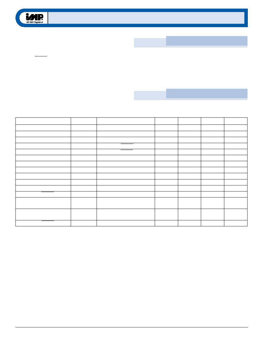
Family Selection Guide

Pin Configuration
I M P 1
I M P 1
2 3 3 D
2 3 3 D
2
408-432-9100/www.impweb.com
2000 © IMP, Inc.
!
Pin Descriptions
IMP1233D-X
RESET
V
CC
GND
1
2
3
GND
4
1233D_03.eps
Package Marking Code
Ordering Information
SOT-223
1233D_05a.eps
1
2
4
3
A
B
C
D
e
g
a
k
c
a
P
e
d
o
C
r
e
t
t
e
L
t
r
a
P
e
p
y
T
e
g
a
k
c
a
P
e
d
o
C
r
e
t
t
e
L
t
e
s
e
R
e
c
n
a
r
e
l
o
T
A
B
C
D
3
3
D
D
3
3
2
1
P
M
I
A
%
5
B
%
0
1
C
%
5
1
y
r
a
m
m
u
S
e
c
i
v
e
D
g
n
i
k
r
a
M
e
g
a
k
c
a
P
*
*
t
r
a
P
r
e
b
m
u
N
T
E
S
E
R
t
u
p
t
u
O
e
g
a
t
l
o
V
)
V
(
T
E
S
E
R
e
c
n
a
r
e
l
o
T
)
%
(
T
E
S
E
R
e
m
i
T
)
s
m
(
e
g
a
t
S
t
u
p
t
u
O
3
2
2
-
T
O
S
e
g
a
k
c
a
P
T
E
S
E
R
y
t
i
r
a
l
o
P
A
B
C
D
*
n
i
a
r
D
-
n
e
p
O
ll
u
P
-
h
s
u
P
%
5
=
A
%
0
1
=
B
%
5
1
=
C
T
/
5
-
Z
D
3
3
2
1
P
M
I
5
2
6
.
4
5
0
5
3
"
"
W
O
L
3
3
D
A
T
/
0
1
-
Z
D
3
3
2
1
P
M
I
5
7
3
.
4
0
1
0
5
3
"
"
W
O
L
3
3
D
B
T
/
5
1
-
Z
D
3
3
2
1
P
M
I
5
2
1
.
4
5
1
0
5
3
"
"
W
O
L
3
3
D
C
k
5
l
a
n
r
e
t
n
I
*
.
p
u
l
l
u
p
r
o
t
s
i
s
e
r
.
l
e
e
R
d
n
a
e
p
a
T
s
e
t
a
c
i
d
n
i
T
/
*
*
s
p
e
.
3
0
t
_
D
3
3
2
1
s
r
e
b
m
u
N
n
i
P
e
m
a
N
n
o
i
t
c
n
u
F
3
2
2
-
T
O
S
2
9
-
O
T
1
1
D
N
G
d
n
u
o
r
G
2
2
T
E
S
E
R
t
u
p
t
u
o
t
e
s
e
r
W
O
L
e
v
i
t
c
A
3
3
V
C
C
t
u
p
n
i
y
l
p
p
u
s
r
e
w
o
P
4
--
D
N
G
)
y
l
n
O
3
2
2
-
T
O
S
(
d
n
u
o
r
G
Absolute Maximum Ratings
I M P 1
I M P 1
2 3 3 D
2 3 3 D
2000 © IMP, Inc.
Microprocessor Supervisor
3
Electrical Characteristics
Voltage on V
CC
. . . . . . . . . . . . . . . . . . . . . . . . ≠0.5V to 7V
Voltage on RESET . . . . . . . . . . . . . . . . . . . . . ≠0.5V to V
CC
+ 0.5V
Operating Temperature Range . . . . . . . . . . . ≠40
∞C to 85∞C
Soldering Temperature . . . . . . . . . . . . . . . . . . 260
∞C for 10 seconds
Storage Temperature . . . . . . . . . . . . . . . . . . . ≠55
∞C to 125∞C
Voltages measured with respect to ground.
These are stress ratings only and functional operation is not implied.
Parameter
Symbol
Conditions
Min
Typ
Max
Units
Supply Voltage
V
CC
1.2
5.5
V
Output Voltage
V
OH
I
OUT
< 500
µA
V
CC
≠ 0.5V
V
CC
≠ 0.1V
V
Output Current
I
OL
Output = 0.4V, V
CC
2.7V
+8
mA
Operating Current
I
CC
V
CC
< 5.5V, RESET output open
8
20
µA
Operating Current
I
CC
V
CC
3.6V, RESET output open
6
15
µA
V
CC
Trip Point (IMP1233D-5)
V
CCTP
4.50
4.625
4.74
V
V
CC
Trip Point (IMP1233D-10)
V
CCTP
4.25
4.375
4.49
V
V
CC
Trip Point (IMP1233D-15)
V
CCTP
4.00
4.125
4.24
V
Internal Pull-Up Resistor
R
P
3.5
5.0
7.5
k
Output Capacitance
C
OUT
10
pF
RESET Active Time
t
RESET
250
350
450
ms
V
CC
Detect to RESET Low
t
RPD
2
5
µs
V
CC
Slew Rate
t
F
300
µs
(V
HTL
- V
LTL
)
V
CC
Slew Rate
t
R
0
ns
(V
LTL
- V
HTL
)
V
CC
Detect to RESET High
t
RPU
t
R
= 5
µs
250
350
450
ms
Unless otherwise noted, V
CC
= 1.2V to 5.5V and specifications are over the operating temperature range of ≠ 40
∞C to +85∞C.
All voltages are referenced to ground.

I M P 1
I M P 1
2 3 3 D
2 3 3 D
4
408-432-9100/www.impweb.com
2000 © IMP, Inc.
!
Operation ≠ Power Monitor
The IMP1233D detects out-of-tolerance power supply conditions.
It resets a processor during power-up and issues a reset to the sys-
tem processor when the monitored power supply voltage is below
the reset threshold (power-down). When an out-of-tolerance V
CC
voltage is detected, the RESET signal is asserted. On power-up,
RESET is kept active (LOW) for approximately 350ms after the
power supply voltage has reached the selected tolerance. This
allows the power supply and microprocessor to stabilize before
RESET is released.
Figure 1. Timing Diagram: Power-Up
Figure 2. Timing Diagram: Power-Down
V
CCTP
(MAX)
V
CCTP
V
CCTP
(MIN)
V
CC
RESET
t
R
t
RPU
V
OH
1233D_06.eps
V
CCTP
(MAX)
V
CCTP
V
CCTP
(MIN)
V
CC
RESET
t
F
V
OL
t
RPD
1233D_07.eps
Application Information
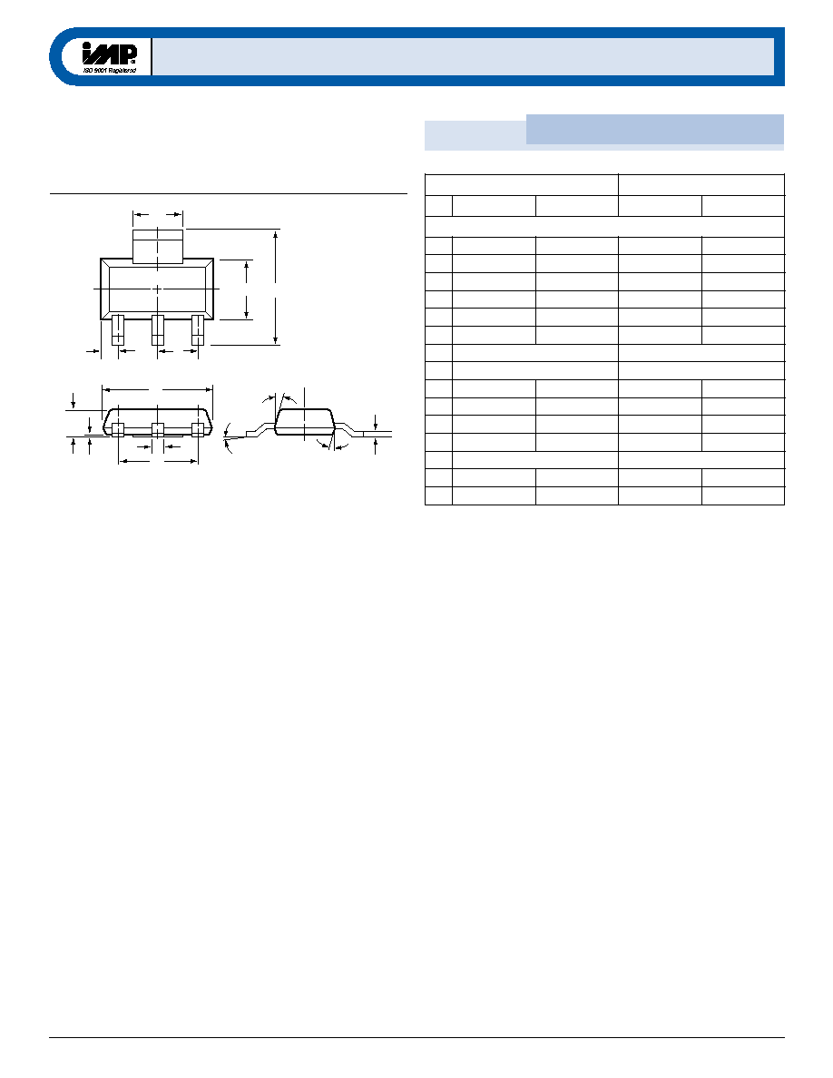
Package Dimensions
I M P 1
I M P 1
2 3 3 D
2 3 3 D
2000 © IMP, Inc.
Microprocessor Supervisor
5
Plastic SOT-223 (4-Pin)
E
A
e1
A1
C
H
e
D
S
B1
B
Q2
Q1
Q
SOT-223 (4-Pin).eps
s
e
h
c
n
I
s
r
e
t
e
m
i
ll
i
M
n
i
M
x
a
M
n
i
M
x
a
M
)
n
i
P
-
4
(
*
3
2
2
-
T
O
S
c
i
t
s
a
l
P
A
7
6
0
.
0
0
6
0
.
0
0
7
.
1
0
5
.
1
1
A
4
0
0
.
0
8
0
0
0
.
0
0
1
.
0
2
0
.
0
B
4
2
1
.
0
6
1
1
.
0
5
1
.
3
5
9
.
2
1
B
3
3
0
.
0
6
2
0
.
0
5
8
.
0
5
6
.
0
C
4
1
0
.
0
0
1
0
.
0
5
3
.
0
5
2
.
0
D
4
6
2
.
0
8
4
2
.
0
0
7
.
6
0
3
.
6
e
M
O
N
5
0
9
0
.
0
M
O
N
0
3
.
2
1
e
M
O
N
1
8
1
.
0
M
O
N
0
5
.
4
E
6
4
1
.
0
0
3
1
.
0
0
7
.
3
0
3
.
3
h
7
8
2
.
0
4
6
2
.
0
0
3
.
7
0
7
.
6
S
1
4
0
.
0
3
3
0
.
0
5
0
.
1
5
8
.
0
t
1
5
0
.
0
3
4
0
.
0
0
3
.
1
0
1
.
1
Q
X
A
M
∞
0
1
X
A
M
∞
0
1
1
Q
∞
6
1
∞
0
1
∞
6
1
∞
0
1
2
Q
∞
6
1
∞
0
1
∞
6
1
∞
0
1
*
.
d
r
a
d
n
a
t
s
e
r
a
s
d
a
e
l
d
e
m
r
o
F
s
p
e
.
5
0
t
_
D
3
3
2
1

IMP, Inc.
Corporate Headquarters
2830 N. First Street
San Jose, CA 95134-2071
Tel: 408-432-9100
Tel: 800-438-3722
Fax: 408-434-0335
e-mail: info@impinc.com
http://www.impweb.com
The IMP logo is a registered trademark of IMP, Inc.
All other company and product names are trademarks of their respective owners.
2000 © IMP, Inc.
Printed in USA
Publication #: 1012
Revision:
B
Issue Date:
06/01/00
Type:
Preliminary
I M P 1
I M P 1
2 3 3 D
2 3 3 D