 | –≠–ª–µ–∫—Ç—Ä–æ–Ω–Ω—ã–π –∫–æ–º–ø–æ–Ω–µ–Ω—Ç: IMP183834 | –°–∫–∞—á–∞—Ç—å:  PDF PDF  ZIP ZIP |
©
1999 IMP, Inc.
408-432-9100/www.impweb.com
1
Key Features
x
Lower power, pin-compatible replacements for
the Dallas DS1834
-- 40% lower maximum supply current:
30µA vs 50µA
x
Monitor 5V and 3.3V supplies simultaneously
x
5V and 3.3V power-on reset
x
350ms reset time
x
Debounced pushbutton reset input
x
Push-Pull CMOS output
-- IMP1834, IMP1834D
-- Eliminates external pull-up resistors
-- Active LOW (IMP1834), HIGH (IMP1834D)
x
Open drain output
-- IMP1834A
-- Active LOW
x
Selectable 5V and 3.3V trip point tolerance
x
Internal power drawn from highest input
voltage, 5V or 3.3V
x
Precision temperature-compensated voltage
reference and comparator
x
Low-cost surface mount SO, compact
MicroSO and DIP packages
x
Wide operating temperature, ≠40
∞
C to +85
∞
C
Block Diagram
3.3V
IN
8
1834_01.eps
40k
5V
IN
5VTOL
5V Tolerance
Bias
IMP1834
PBRST
1
3
≠
+
Low TC
Reference
3.3VTOL
5
6
GND
4
5VRESET
5VRESET (IMP1834D)
For IMP1834D
350 ms
Delay
For IMP1834D
3.3V Tolerance
Bias
2
≠
+
3.3VRESET
3.3VRESET (IMP1834D)
350 ms
Delay
7
Pushbutton Level
Sense and Debounce
IMP1
IMP1
83
83
4/A/D
4/A/D
P
OWER
M
ANAGEMENT
Dual 5V and 3.3V
Dual 5V and 3.3V
µ
µ
P P
P P
o
o
w
w
er
er
Suppl
Suppl
y Super
y Super
visor
visor
s w/Manual R
s w/Manual R
eset
eset
≠ Push-Pull and Open-Dr
≠ Push-Pull and Open-Dr
ain Outputs
ain Outputs
≠ Select
≠ Select
able T
able T
r
r
ip P
ip P
oint T
oint T
oler
oler
ance
ance
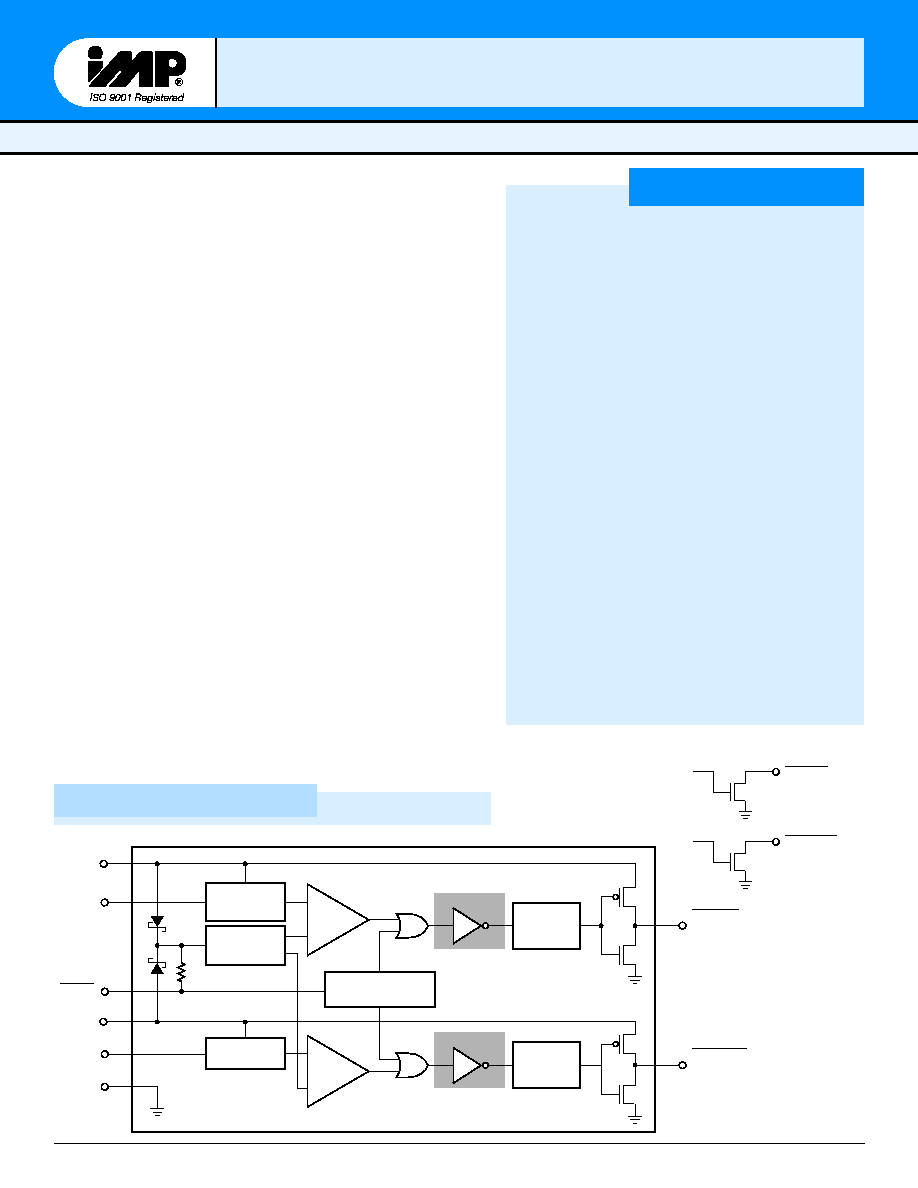
The IMP1834 supervisors simultaneously monitor both 3.3V and 5V
power sources and issue reset signals when either supply is out of toler-
ance. When an out-of-tolerance condition is detected, the output-reset
signal of the affected supply becomes active and resets the system micro-
processor/microcontroller. On power-up and after the supply voltage
returns to an in-tolerance condition, the reset signal remains active for
approximately 350ms. This allows the power supply and system micro-
processor to stabilize.
The IMP1834 supervisors are pin-compatible with devices from Dallas
Semiconductor and require up to 40% less current.
Tolerance levels are independently selectable for both supplies.
Tolerance options are 5- and 10-percent for the 5V supply and for the
3.3V supply, 10- and 20-percent.
The IMP1834 and IMP1834D have push-pull reset output stages. The
IMP1834A active LOW reset outputs are open drain devices that can
both be connected to either 5 volt or 3.3 volt supply. The IMP1834 and
IMP1834A have active LOW reset outputs. The IMP1834D has active
HIGH reset outputs.
All devices can issue reset signals through an internally debounced
pushbutton reset input that affects both reset outputs.
All devices operate over the extended industrial temperature range.
Devices are available in 8-pin DIP, surface mount 8-pin SO and 8-pin
MicroSO packages. Die are also available.
1834_02.eps
5VRESET
2
3.3VRESET
7
IMP1834A
r
e
b
m
u
N
n
i
P
e
m
a
N
n
o
i
t
c
n
u
F
1
V
5
N
I
.
t
u
p
n
i
y
l
p
p
u
s
r
e
w
o
p
V
5
2
T
E
S
E
R
V
5
T
E
S
E
R
V
5
.
)
A
4
3
8
1
P
M
I
r
o
f
s
t
u
p
t
u
o
n
i
a
r
d
n
e
p
O
.
A
4
3
8
1
P
M
I
,
4
3
8
1
P
M
I
,
W
O
L
e
v
i
t
c
A
(
t
u
p
t
u
o
t
e
s
e
r
V
5
.
)
D
4
3
8
1
P
M
I
,
H
G
I
H
e
v
i
t
c
A
(
t
u
p
t
u
o
t
e
s
e
r
V
5
3
L
O
T
V
5
V
5
L
O
T
V
5
r
o
f
e
c
n
a
r
e
l
o
t
%
0
1
:
t
c
e
l
e
s
e
c
n
a
r
e
l
o
t
t
u
p
n
i
V
5
N
I
.
D
N
G
=
L
O
T
V
5
r
o
f
e
c
n
a
r
e
l
o
t
%
5
d
n
a
4
D
N
G
.
d
n
u
o
r
G
5
T
S
R
B
P
k
0
4
(
t
u
p
n
i
t
e
s
e
r
n
o
t
t
u
b
h
s
u
p
l
a
u
n
a
m
d
e
c
n
u
o
b
e
D
.
)
p
u
ll
u
p
l
a
n
r
e
t
n
i
6
L
O
T
V
3
.
3
V
3
.
3
=
L
O
T
V
3
.
3
r
o
f
e
c
n
a
r
e
l
o
t
%
0
2
:
t
c
e
l
e
s
e
c
n
a
r
e
l
o
t
t
u
p
n
i
V
3
.
3
N
I
r
o
f
e
c
n
a
r
e
l
o
t
%
0
1
d
n
a
,
.
D
N
G
=
L
O
T
V
3
.
3
7
T
E
S
E
R
V
3
.
3
T
E
S
E
R
V
3
.
3
.
)
A
4
3
8
1
P
M
I
r
o
f
s
t
u
p
t
u
o
n
i
a
r
d
n
e
p
O
.
A
4
3
8
1
P
M
I
,
4
3
8
1
P
M
I
,
W
O
L
e
v
i
t
c
A
(
t
u
p
t
u
o
t
e
s
e
r
V
3
.
3
.
)
D
4
3
8
1
P
M
I
,
H
G
I
H
e
v
i
t
c
A
(
t
u
p
t
u
o
t
e
s
e
r
V
3
.
3
8
V
3
.
3
N
I
.
t
u
p
n
i
y
l
p
p
u
s
r
e
w
o
p
V
3
.
3
s
p
e
.
t
1
0
_
4
3
8
1
2
408-432-9100/www.impweb.com
©
1999 IMP, Inc.
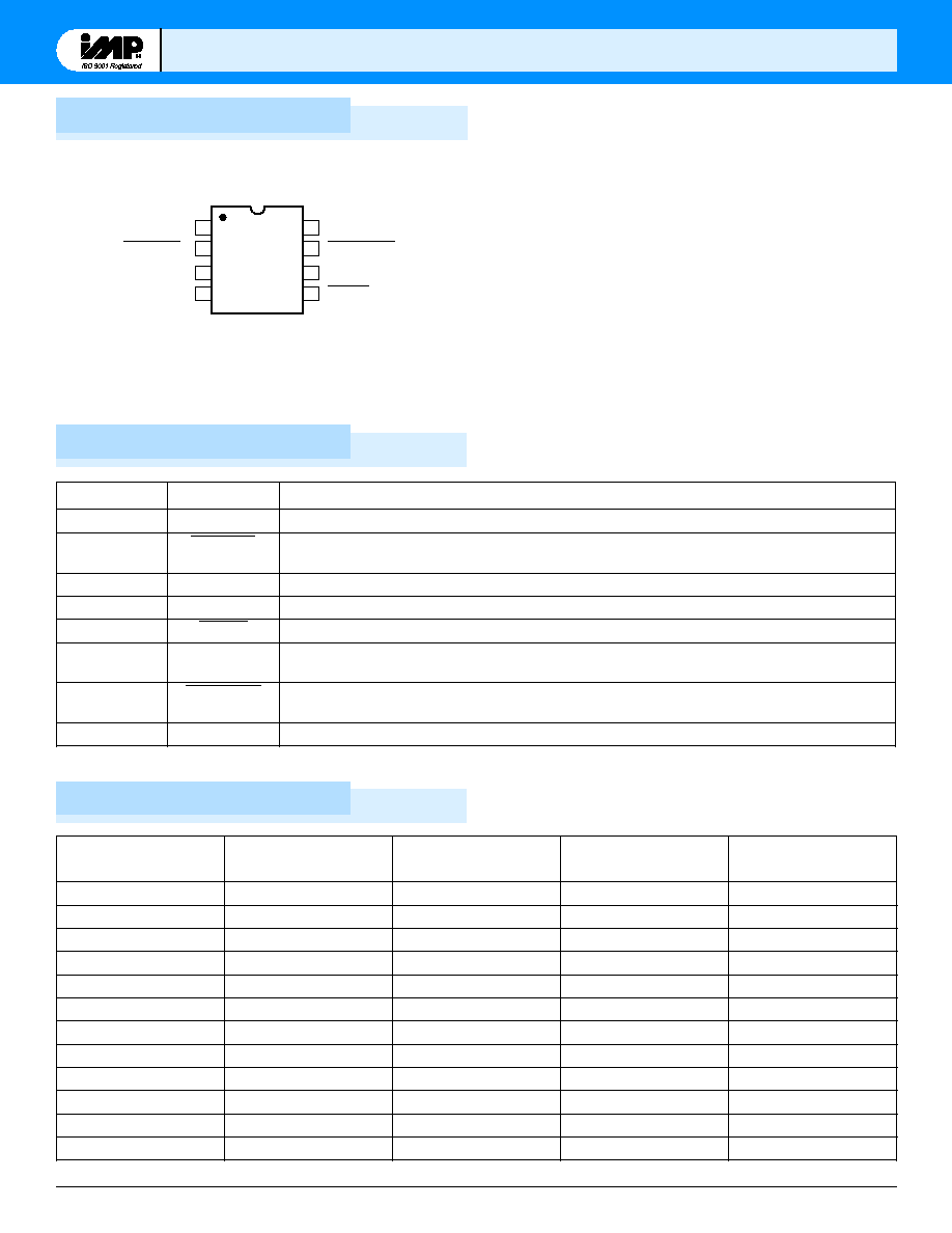
Pin Configuration
IMP1
IMP1
83
83
4/A/D
4/A/D
Pin Descriptions
IMP1834
IMP1834A
IMP1834D
1
2
3
4
5V
IN
5VRESET*
5VTOL
GND
3.3V
IN
3.3VRESET*
3.3VTOL
PBRST
8
7
6
5
1834_03.eps
* IMP1834D reset outputs are
active HIGH (5VRESET and 3.3VRESET).
Outputs are open drain for IMP1834A.
Ordering Information
DIP/SO/MicroSO
r
e
b
m
u
N
t
r
a
P
e
g
a
k
c
a
P
g
n
i
t
a
r
e
p
O
e
g
n
a
R
e
r
u
t
a
r
e
p
m
e
T
y
t
i
r
a
l
o
P
t
e
s
e
R
e
g
a
t
S
t
u
p
t
u
O
4
3
8
1
P
M
I
P
I
D
-
8
≠ 0
4 ∞
5
8
o
t
C
∞C
W
O
L
ll
u
P
-
h
s
u
P
A
M
E
4
3
8
1
P
M
I
O
S
o
r
c
i
M
≠ 0
4 ∞
5
8
o
t
C
∞C
W
O
L
ll
u
P
-
h
s
u
P
S
4
3
8
1
P
M
I
O
S
-
8
≠ 0
4 ∞
5
8
o
t
C
∞C
W
O
L
ll
u
P
-
h
s
u
P
D
/
4
3
8
1
P
M
I
E
C
I
D
5
2 ∞C
W
O
L
ll
u
P
-
h
s
u
P
A
4
3
8
1
P
M
I
P
I
D
-
8
≠ 0
4 ∞
5
8
o
t
C
∞C
W
O
L
n
i
a
r
D
n
e
p
O
A
M
E
A
4
3
8
1
P
M
I
O
S
o
r
c
i
M
≠ 0
4 ∞
5
8
o
t
C
∞C
W
O
L
n
i
a
r
D
n
e
p
O
S
A
4
3
8
1
P
M
I
O
S
-
8
≠ 0
4 ∞
5
8
o
t
C
∞C
W
O
L
n
i
a
r
D
n
e
p
O
D
/
A
4
3
8
1
P
M
I
E
C
I
D
5
2 ∞C
W
O
L
n
i
a
r
D
n
e
p
O
D
4
3
8
1
P
M
I
P
I
D
-
8
≠ 0
4 ∞
5
8
o
t
C
∞C
H
G
I
H
ll
u
P
-
h
s
u
P
A
M
E
D
4
3
8
1
P
M
I
O
S
o
r
c
i
M
≠ 0
4 ∞
5
8
o
t
C
∞C
H
G
I
H
ll
u
P
-
h
s
u
P
S
D
4
3
8
1
P
M
I
O
S
-
8
≠ 0
4 ∞
5
8
o
t
C
∞C
H
G
I
H
ll
u
P
-
h
s
u
P
D
/
D
4
3
8
1
P
M
I
E
C
I
D
5
2 ∞C
H
G
I
H
ll
u
P
-
h
s
u
P
s
p
e
.
t
2
0
_
4
3
8
1
©
1999 IMP, Inc.
408-432-9100/www.impweb.com
3
IMP1
IMP1
83
83
4/A/D
4/A/D
Absolute Maximum Ratings
Electrical Characteristics
Voltage on V
IN
pins . . . . . . . . . . . . . . . . ≠0.5V to 7V
Voltage on 5VRESET . . . . . . . . . . . . . . . ≠0.5V to (+5V
IN
+0.5V)
(IMP1834, IMP1834D)
Voltage on 3.3VRESET . . . . . . . . . . . . . . ≠0.5V to (+3.3V
IN
+0.5V)
(IMP1834, IMP1834D)
Voltage on PBRST and reset outputs . . ≠0.5V to the greater of
5V
IN
+0.5V or 3.3V
IN
+0.5V
(IMP1834A)
Operating Temperature Range . . . . . . . ≠40
∞
C to 85
∞
C
Storage Temperature . . . . . . . . . . . . . . . ≠55
∞
C to 125
∞
C
Soldering Temperature . . . . . . . . . . . . . . 260
∞
C for 10 seconds
Voltages measured with respect to ground.
These are stress ratings only and functional operation is not implied.
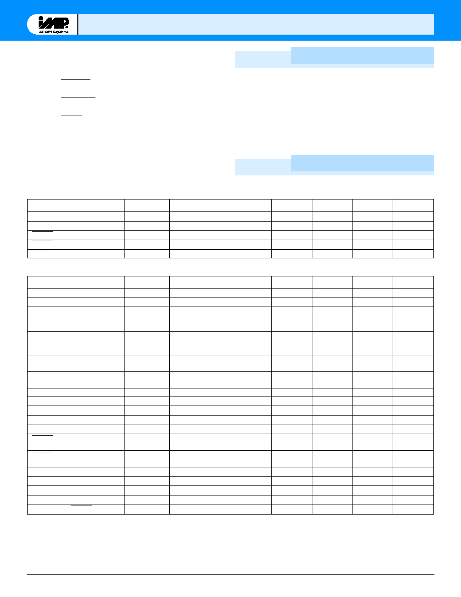
Parameter
Symbol
Conditions
Min
Typ
Max
Units
5V Supply Voltage (5V
IN
)
5V
IN
1.2
5.5
V
3.3V Supply Voltage (3.3V)
3.3V
IN
1.2
5.5
V
PBRST Input High Level
V
IH
Both 3.3V
IN
and 5V
IN
2.7V
2
V
INMAX
+ 0.3V
V
PBRST Input High Level
V
IH
Both 3.3V
IN
and 5V
IN
2.7V
V
INMAX
≠ 0.4V
V
PBRST Input Low Level
V
IL
≠ 0.3
0.5
V
Recommended DC operating condition over the operating temperature range of ≠40
∞
C to +85
∞
C.
All voltages are referenced to ground.
Parameter
Symbol
Conditions
Min
Typ
Max
Units
Output Voltage
V
OH
V
IN
≠ 0.1V
V
Input Leakage
I
IL
≠1.0
+1.0
µ
A
Output Current
I
OH
Output = 2.4V. Either 3.3V
IN
or
350
µ
A
5V
IN
2.7V.
(IMP1834/1834D only)
Output Current
I
OL
Output = 0.4V. Either 3.3V
IN
or
+10
mA
5V
IN
2.7V.
(IMP1834/1834D only)
5V Operating Current
I
CC
3.3V
IN
and 5V
IN
5.5V, 16
30
µ
A
RESET outputs open.
3.3V Operating Current
I
CC
3.3V
IN
and 5V
IN
3.6V, 12
25
µ
A
RESET outputs open.
5V Trip Point
V
INTP
5VTOL = GND
4.50
4.63
4.75
V
5V Trip Point
V
INTP
5VTOL = 5V
IN
4.25
4.38
4.49
V
3.3V Trip Point
V
INTP
3.3VTOL = GND
2.80
2.88
2.97
V
3.3V Trip Point
V
INTP
3.3VTOL = 3.3V
IN
2.47
2.55
2.64
V
Output Capacitance
C
OUT
10
pF
PBRST Manual Reset
t
PB
2
ms
Minimum Low Time
PBRST Stable LOW to
t
PDLY
2
ms
Reset Active
Reset Active Time
t
RST
200
350
500
ms
V
CC
Detect Noise Immunity
t
RPD
2
µ
s
V
CC
Slew Rate
t
F
V
INTP
(MAX) to V
INTP
(MIN)
300
µ
s
V
CC
Slew Rate
t
R
V
INTP
(MIN) to V
INTP
(MAX)
0
ns
V
CC
Detect to RESET or RESET
t
RPU
t
rise
= 5
µ
s
200
350
500
ms
Unless otherwise noted, V
IN
= 1.2V to 5.5V and specifications are over the operating temperature range of ≠40
∞
C to +85
∞
C.
4
408-432-9100/www.impweb.com
©
1999 IMP, Inc.
IMP1
IMP1
83
83
4/A/D
4/A/D
Application Information
Operation ≠ Power Monitor
The IMP1834 supervisors simultaneously detect out-of-tolerance
power supply conditions on both 3.3V and 5V power supplies. If
the voltages at 5V
IN
or 3.3V
IN
are outside the tolerance band, the
reset for the failing supply voltage becomes active. When the moni-
tored supply returns to an in-tolerance state, the reset remains active
for approximately 350ms before returning to the inactive state.
On power-up, the reset signals are kept active for approximately
350ms after the power supply voltages have reached the selected
tolerance. This allows the power supply and microprocessor to
stabilize before the reset is removed.
All supply current for the IMP1834 devices is drawn from the
input (5V
IN
or 3.3V
IN
) with the highest voltage level. The outputs
draw current from their input supplies 5V
IN
and 3.3V
IN
.
Reset Signal Polarity and Output Stage Structure
The IMP1834 and IMP1834A supervisors have active LOW reset
signals. The IMP1834D reset outputs are active HIGH.
The IMP1834 and IMP1834D have CMOS push-pull output
stages. The IMP1834A has open drain reset outputs.
Output Stage
IMP Part
RESET Polarity
Configuration
IMP1834
LOW
Push-Pull
IMP1834EMA
LOW
Push-Pull
IMP1834S
LOW
Push-Pull
IMP1834A
LOW
Open Drain
IMP1834AEMA
LOW
Open Drain
IMP1834AS
LOW
Open Drain
IMP1834D
HIGH
Push-Pull
IMP1834DEMA
HIGH
Push-Pull
IMP1834DS
HIGH
Push-Pull
Trip Point Tolerance Selection
The 3.3VTOL and 5VTOL inputs allow independent selection of
the reset trip points. If 5VTOL is connected to the 5V supply input,
a 10% tolerance is selected. If 5VTOL is grounded, a 5% tolerance
is selected.
If 3.3VTOL is connected to the 3.3V supply input, a 20% tolerance
is selected. If 3.3VTOL is grounded, a 10% tolerance is selected.
See Table 1.
The 3.3VTOL and 5VTOL tolerance select inputs should be tied to
ground or to the respective input supply voltage pin, 3.3V
IN
or 5V
IN
.
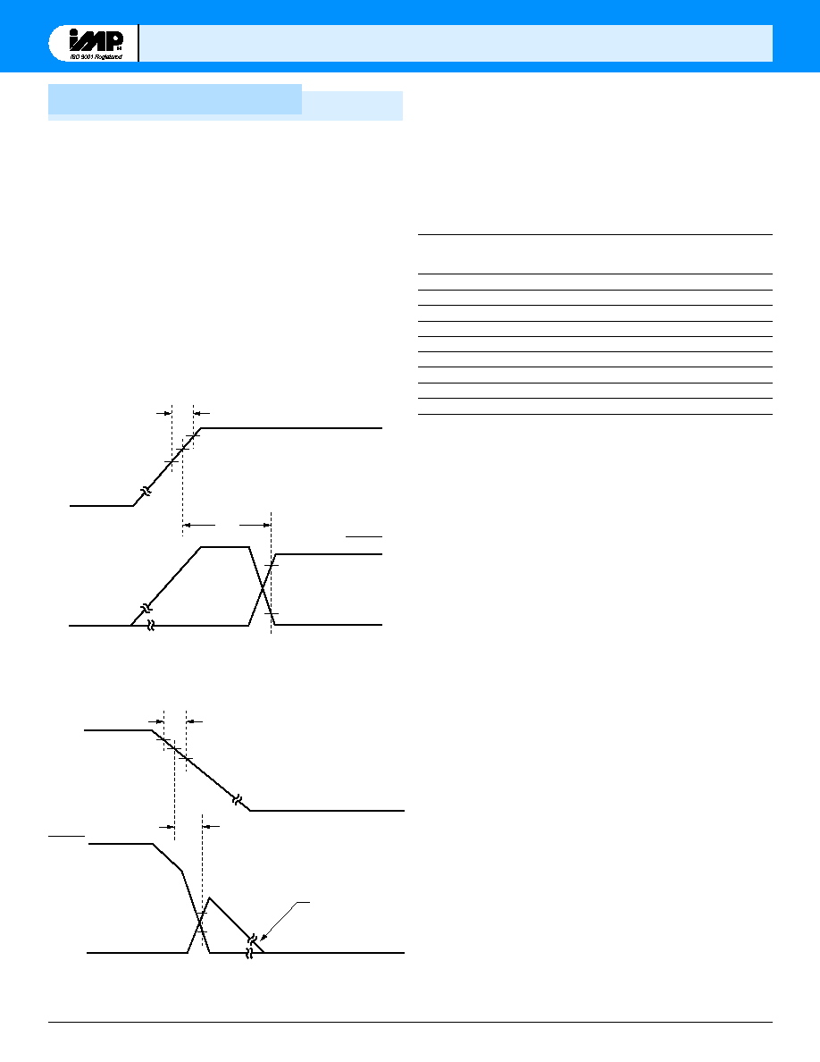
Figure 1. Timing Diagram: Power Up
Figure 2. Timing Diagram: Power Down
(IMP1834D Only)
1834_10.eps
V
INTP
(Max)
V
INTP
V
INTP
(Min)
V
IN
RESET
RESET
t
R
t
RPU
V
OH
V
OL
V
INTP
V
INTP
(Max)
V
INTP
(Min)
V
IN
RESET
RESET
> t
RPD
t
F
V
OH
V
OL
RESET Slews
with V
CC
1834_09.eps
(IMP1834D Only)
IMP1
IMP1
83
83
4/A/D
4/A/D
Application Information
©
1999 IMP, Inc.
408-432-9100/www.impweb.com
5
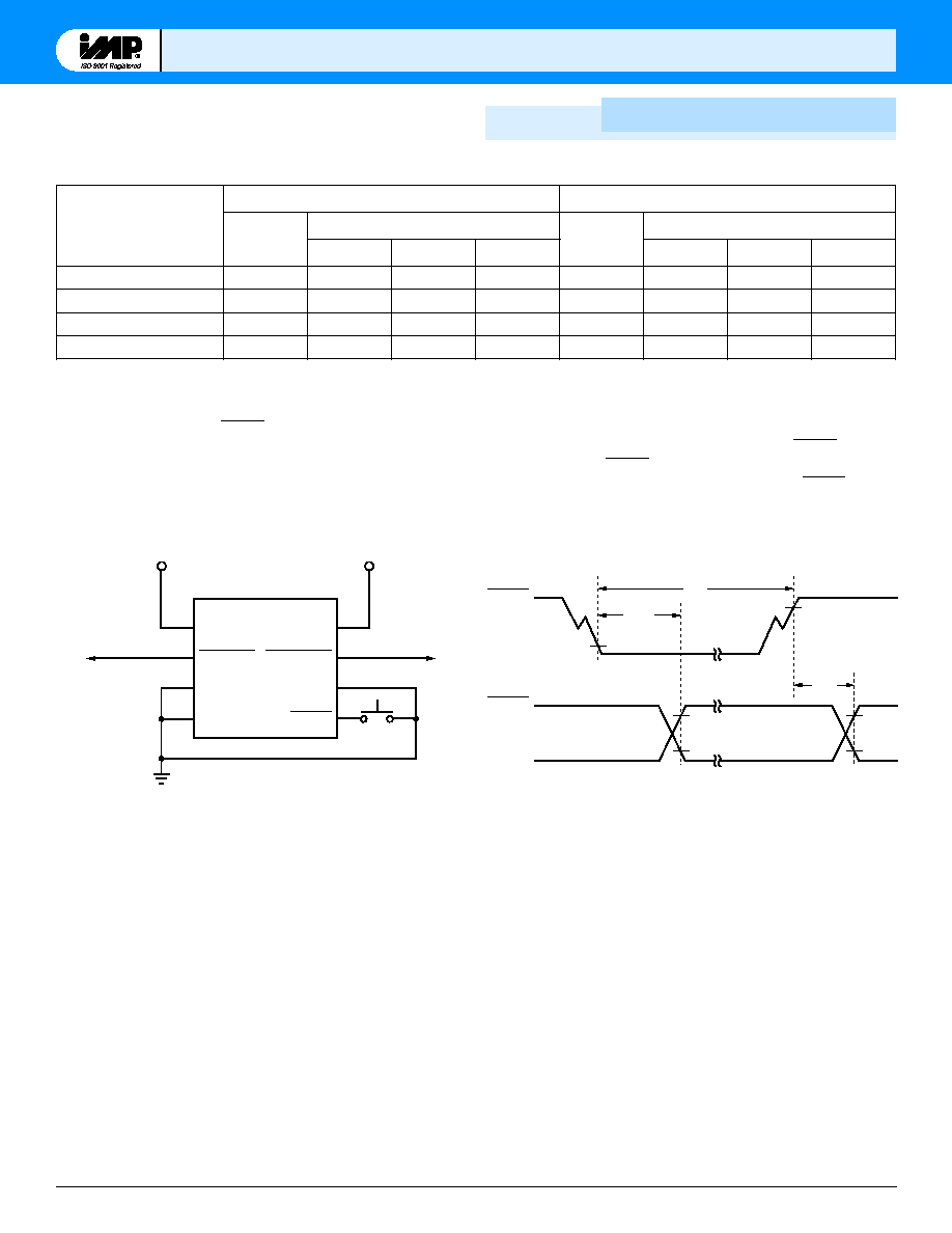
Manual Reset Operation
Pushbutton switch input, PBRST, allows the user to override the
internal trip point detection circuits and issue reset signals. The
pushbutton input is debounced and is pulled HIGH through a
40k
, internal pull-up resistor.
When at least one of the reset outputs is not asserted, a pushbut-
ton initiated reset signal can be issued by holding PBRST LOW for
at least 2ms. When PBRST is held LOW, both resets become active
and remain active for approximately 350ms after PBRST returns
HIGH. See Figure 3 and Figure 4.
t
c
e
l
e
S
e
c
n
a
r
e
l
o
T
t
u
p
n
I
V
3
.
3
t
u
p
n
I
V
5
V
3
.
3
e
c
n
a
r
e
l
o
T
)
V
(
t
n
i
o
P
P
I
R
T
V
5
e
c
n
a
r
e
l
o
T
)
V
(
t
n
i
o
P
P
I
R
T
N
I
M
l
a
n
i
m
o
N
X
A
M
N
I
M
l
a
n
i
m
o
N
X
A
M
V
5
=
L
O
T
V
5
N
I
--
--
--
--
%
0
1
5
2
.
4
8
3
.
4
9
4
.
4
D
N
G
=
L
O
T
V
5
--
--
--
--
%
5
5
.
4
3
6
.
4
5
7
.
4
V
3
.
3
=
L
O
T
V
3
.
3
N
I
%
0
2
7
4
.
2
5
5
.
2
4
6
.
2
--
--
--
--
D
N
G
=
L
O
T
V
3
.
3
%
0
1
0
8
.
2
8
8
.
2
7
9
.
2
--
--
--
--
s
p
e
.
t
3
0
_
4
3
8
1
Table 1. Threshold Selection
Figure 3. Pushbutton Reset
1834_04.eps
5V
IN
3.3V
1
3.3V
IN
5VRESET
2
3.3VRESET
5VTOL
IMP1834
3
4
3.3VTOL
GND
8
7
6
5
PBRST
5V
Figure 4. Timing Diagram: Pushbutton Reset
V
IL
V
OH
V
OL
RESET
RESET
PBRST
t
PDLY
t
PB
t
RST
1834_05.eps
V
IH
(IMP1834D)