
©
1999 IMP, Inc.
408-432-9100/www.impweb.com
1
Key Features
Applications
x
High-efficiency linear power supplies
x
Post regulator for switching supplies
x
5V to 3.3V linear regulators
x
USB hubs
x
Battery chargers
x
Routers, ISDN/DSL modems
x
Low Dropout Voltage
≠ 0.8V maximum at 100mA
≠ 0.95V maximum at 800mA
≠ 20% lower dropout voltage than "1117"
LDO regulators
x
Guaranteed Low Dropout Voltage at Multiple
Current Levels
x
1% Trimmed 2.5V, 3.0V and 3.3V Outputs
x
Reduced Quiescent Current: 75µA Maximum
x
Short Circuit and Thermal Protection
x
Space Saving SOT-223 Surface Mount Package
x
"1117" Pin Compatible
Block Diagram
≠
+
+
≠
37_01.eps
GND
1
Ref
IMP37
Thermal
Protection
Error
Amp
Current
Limit
2
Input
3
Out
(Tab)
R
CS
+
≠
IMP3
IMP3
7
7
P
OWER
M
ANAGEMENT
Lo
Lo
w Dr
w Dr
opout P
opout P
ositiv
ositiv
e
e
V
V
olt
olt
ag
ag
e R
e R
egulat
egulat
or
or
s
s
≠ 800mA
≠ 800mA
≠ 2.5V
≠ 2.5V
, 3.0V and 3.3V Output
, 3.0V and 3.3V Output
The IMP37 series of Low Dropout (LDO) three-terminal voltage regula-
tors feature guaranteed low dropout voltages at currents up to 0.8A. The
IMP37 regulator family dropout voltage is guaranteed to be 0.95V or
lower at 0.8A. At 100mA, the maximum dropout voltage is 0.8V.
Compared with "1117" type LDOs, the IMP37 has a 20% lower dropout
voltage.
Three fixed output voltages are offered: 2.5V, 3.0V and 3.3V. Output volt-
ages are factory trimmed to within 1% of the nominal value.
In addition to low dropout voltages, the IMP37 family features greatly
reduced quiescent operating current. The 75
µ
A maximum specification
represents an over 100 times improvement over competitive devices.
Devices are short circuit protected, and a thermal protection circuit shuts
the regulator off should the junction temperature exceed 165∞C.
The IMP37 is available in low-profile plastic SOT-223 and TO-263
packages and are pin compatible with fixed "1117" devices.
2
408-432-9100/www.impweb.com
©
1999 IMP, Inc.
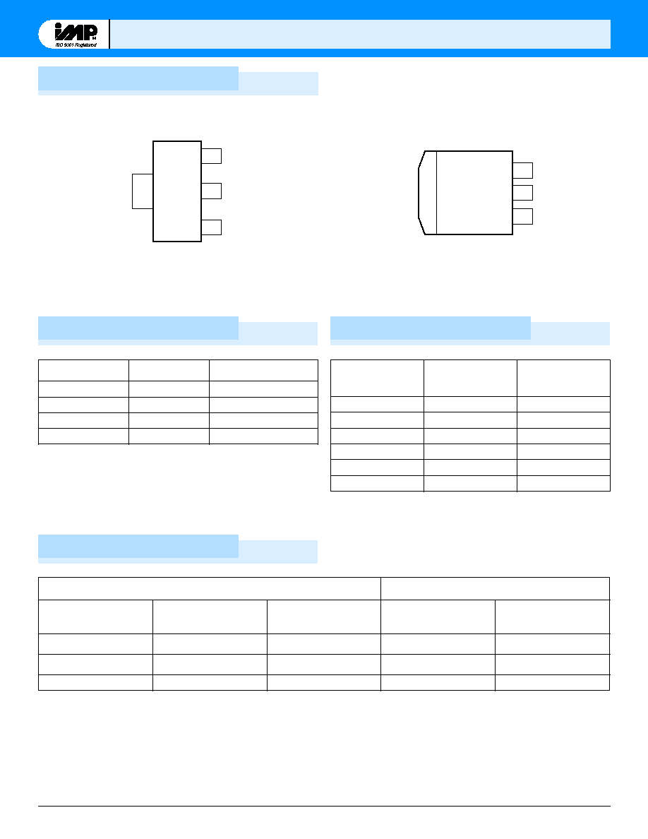
Pin Configuration
IMP3
IMP3
7
7
Pin Descriptions
IMP37
GND
INPUT
TAB IS V
OUT
1
3
OUT
2
37_04.eps
Package Marking Code
Ordering Information
IMP37
37_05.eps
GND
INPUT
1
3
OUT
TAB IS V
OUT
2
SOT-223
TO-263
Front View
Front View
r
e
b
m
u
N
t
r
a
P
e
g
a
k
c
a
P
e
c
i
v
e
D
g
n
i
k
r
a
M
T
S
J
5
2
-
7
3
P
M
I
3
2
2
-
T
O
S
5
2
7
3
T
S
J
0
3
-
7
3
P
M
I
3
2
2
-
T
O
S
0
3
7
3
T
S
J
3
3
-
7
3
P
M
I
3
2
2
-
T
O
S
3
3
7
3
M
C
J
5
2
-
7
3
P
M
I
3
6
2
-
O
T
M
C
J
5
2
7
3
M
C
J
0
3
-
7
3
P
M
I
3
6
2
-
O
T
M
C
J
0
3
7
3
M
C
J
3
3
-
7
3
P
M
I
3
6
2
-
O
T
M
C
J
3
3
7
3
s
p
e
.
5
0
e
l
b
a
T
_
7
3
s
n
o
i
t
p
O
t
u
p
t
u
O
r
e
b
m
u
N
g
n
i
r
e
d
r
O
t
r
a
P
e
g
a
t
l
o
V
m
u
m
i
x
a
M
t
n
e
r
r
u
C
t
n
e
c
s
e
i
u
Q
t
a
e
g
a
t
l
o
V
t
u
o
p
o
r
D
A
m
0
0
8
3
2
2
-
T
O
S
e
g
a
k
c
a
P
3
6
2
-
O
T
e
g
a
k
c
a
P
V
5
.
2
5
7
µ
A
V
5
9
.
0
T
S
J
5
2
-
7
3
P
M
I
M
C
J
5
2
-
7
3
P
M
I
V
0
.
3
5
7
µ
A
V
5
9
.
0
T
S
J
0
3
-
7
3
P
M
I
M
C
J
0
3
-
7
3
P
M
I
V
3
.
3
5
7
µ
A
V
5
9
.
0
T
S
J
3
3
-
7
3
P
M
I
M
C
J
3
3
-
7
3
P
M
I
s
p
e
.
6
0
t
_
7
3
Note: Tape and reel shipping is available for the SOT-223 and TO-263 packages. Append the TAPE AND REEL designation "/T" to the ordering
part number for tape and reel devices. For example, the IMP37-25JST/T is a 2.5V SOT-223 packaged device shipped in reels.
r
e
b
m
u
N
n
i
P
e
m
a
N
n
o
i
t
c
n
u
F
1
D
N
G
n
i
P
d
n
u
o
r
G
2
T
U
O
e
g
a
t
l
o
V
t
u
p
t
u
O
3
T
U
P
N
I
e
g
a
t
l
o
V
t
u
p
n
I
B
A
T
B
A
T
e
g
a
t
l
o
V
t
u
p
t
u
O
s
p
e
.
3
0
e
l
b
a
T
_
7
3

©
1999 IMP, Inc.
408-432-9100/www.impweb.com
3
IMP3
IMP3
7
7
Absolute Maximum Ratings
Electrical Characteristics
Input Voltage . . . . . . . . . . . . . . . . . . . . . . . . . 7V
Operating Junction Temperature . . . . . . . . . 0
∞
C to 150
∞
C
Storage Temperature Range . . . . . . . . . . . . . ≠65
∞
C to +150
∞
C
Lead Temperature (Soldering) . . . . . . . . . . . . . 300
∞
C for 10 seconds
These are stress ratings only and functional operation is not implied.
Exposure to absolute maximum ratings for prolonged time periods may
affect device reliability. All voltages are with respect to ground.
Specifications apply over the junction operating temperature range of T
J
= 0∞C to +125∞C unless otherwise noted.
Notes: 1. See thermal regulation specification for changes in output voltage due to heating effects. Load regulation and line regulation
are measured with low duty cycle pulse testing to maintain a constant junction temperature.
2. Dropout voltage is specified over the full output current range. Dropout voltage is defined as the minimum input/output
differential measured at the specified output current.
3. Minimum load current is defined as the minimum output current required to maintain regulation.
r
e
t
e
m
a
r
a
P
l
o
b
m
y
S
x
if
f
u
S
s
n
o
it
i
d
n
o
C
n
i
M
p
y
T
x
a
M
s
ti
n
U
e
g
a
t
l
o
V
t
u
p
t
u
O
V
T
U
O
5
2
≠
I
T
U
O
V
,
A
m
0
1
=
N
I
T
,
V
5
8
.
4
=
J
5
2
=
C
∞
5
7
4
.
2
5
.
2
5
2
5
.
2
V
A
m
0
1
I
T
U
O
I
X
A
M
V
5
2
.
4
,
V
N
I
V
5
.
5
5
4
.
2
5
.
2
5
5
.
2
0
3
≠
I
T
U
O
V
,
A
m
0
1
=
N
I
T
,
V
5
=
J
5
2
=
C
∞
7
9
.
2
0
0
.
3
3
0
.
3
A
m
0
1
I
T
U
O
I
X
A
M
V
5
7
.
4
,
V
N
I
V
5
.
5
4
9
.
2
0
0
.
3
6
0
.
3
3
3
≠
I
T
U
O
V
,
A
m
0
1
=
N
I
T
,
V
5
=
J
5
2
=
C
∞
7
6
2
.
3
0
3
.
3
3
3
3
.
3
A
m
0
1
I
T
U
O
I
X
A
M
V
5
7
.
4
,
V
N
I
V
5
.
5
5
3
2
.
3
0
3
.
3
5
6
3
.
3
n
o
i
t
a
l
u
g
e
R
e
n
i
L
)
1
e
t
o
N
(
5
2
≠
I
T
U
O
V
5
2
.
4
,
A
m
0
1
=
(
V
N
I
)
V
5
.
5
2
1
9
1
V
m
0
3
≠
I
T
U
O
V
5
.
4
,
A
m
0
1
=
V
N
I
V
5
.
5
2
1
9
1
3
3
≠
I
T
U
O
V
5
.
4
,
A
m
0
1
=
V
N
I
V
5
.
5
2
1
9
1
n
o
i
t
a
l
u
g
e
R
e
n
i
L
)
1
e
t
o
N
(
5
2
≠
I
T
U
O
V
5
2
.
4
,
A
m
0
1
=
(
V
N
I
)
T
,
V
5
.
5
A
5
2
=
C
∞
8
.
2
3
.
4
V
m
0
3
≠
I
T
U
O
V
5
.
4
,
A
m
0
1
=
V
N
I
T
,
V
5
.
5
A
5
2
=
C
∞
8
.
2
3
.
4
3
3
≠
I
T
U
O
V
5
.
4
,
A
m
0
1
=
V
N
I
T
,
V
5
.
5
A
5
2
=
C
∞
8
.
2
3
.
4
n
o
i
t
a
l
u
g
e
R
d
a
o
L
)
1
e
t
o
N
(
5
2
≠
V
N
I
A
m
5
,
V
5
2
.
4
=
I
T
U
O
A
m
0
0
8
5
2
0
3
V
m
0
3
≠
V
N
I
A
m
5
,
V
5
7
.
4
=
I
T
U
O
A
m
0
0
8
5
2
0
3
3
3
≠
V
N
I
A
m
5
,
V
5
7
.
4
=
I
T
U
O
A
m
0
0
8
5
2
0
3
e
g
a
t
l
o
V
t
u
o
p
o
r
D
)
2
e
t
o
N
(
x
x
≠
I
T
U
O
A
m
0
0
1
=
8
.
0
V
I
T
U
O
A
m
0
0
8
=
5
9
.
0
t
i
m
i
L
t
n
e
r
r
u
C
I
)
X
A
M
(
T
U
O
x
x
≠
T
J
5
2
=
C
∞
0
0
8
0
5
9
0
0
2
1
A
m
t
n
e
r
r
u
C
d
a
o
L
m
u
m
i
n
i
M
x
x
≠
0
.
5
A
m
t
n
e
r
r
u
C
t
n
e
c
s
e
i
u
Q
I
Q
x
x
≠
V
N
I
V
6
6
3
5
7
µ
A
n
o
i
t
a
l
u
g
e
R
l
a
m
r
e
h
T
T
A
5
2
=
C
∞
e
s
l
u
P
s
m
0
3
,
1
0
.
0
1
.
0
W
/
%
n
o
i
t
c
e
j
e
R
e
l
p
p
i
R
f
E
L
P
P
I
R
V
,
z
H
0
2
1
=
N
I
T
,
V
5
=
A
5
2
=
C
∞
V
E
L
P
P
I
R
I
,
p
-
p
V
1
=
D
A
O
L
A
m
0
1
=
1
5
4
5
B
d
y
t
il
i
b
a
t
S
e
r
u
t
a
r
e
p
m
e
T
5
.
0
%
y
t
il
i
b
a
t
S
m
r
e
T
g
n
o
L
T
A
5
2
1
=
C
∞
s
r
H
0
0
0
1
,
3
.
0
%
e
s
i
o
N
t
u
p
t
u
O
S
M
R
V
f
o
%
(
T
U
O
z
H
0
1
,
)
f
T
,
z
H
k
0
1
J
5
2
=
C
∞
3
0
0
.
0
%
e
c
n
a
t
s
i
s
e
R
l
a
m
r
e
h
T
)
3
2
2
-
O
T
(
B
A
T
t
a
e
s
a
C
-
o
t
-
n
o
i
t
c
n
u
J
5
1
∞
W
/
C
)
3
6
2
-
O
T
(
B
A
T
t
a
e
s
a
C
-
o
t
-
n
o
i
t
c
n
u
J
0
1
s
p
e
.
7
0
t
_
7
3

4
408-432-9100/www.impweb.com
©
1999 IMP, Inc.
IMP3
IMP3
7
7
Application Information
The IMP37 voltage regulator ICs offer self-protection features
which include short-circuit current protection and automatic thermal
shutdown (for junction temperature above 165∞C).
Circuit Stability
Like all regulators, an output filter capacitor is required for circuit sta-
bility. Besides smoothing the output, the output capacitor
"completes" the regulator's frequency compensation. The ESR of the
output capacitor should be less than 0.5
. Low ESR capacitors are
preferred.
Table 1 shows recommended minimum capacitance values for both
aluminum and tantalum capacitors. Larger values of output capaci-
tance do not cause stability problems.
Table 1. Recommended Output Bypass Capacitors
An input bypass capacitor is recommended. A 10
µ
F or larger tanta-
lum capacitor is suitable for most applications.
5
.
0
<
R
S
E
(
r
o
t
i
c
a
p
a
C
s
s
a
p
y
B
t
u
p
t
u
O
)
0
1
µ
0
0
1
,
m
u
l
a
t
n
a
T
F
µ
m
u
n
i
m
u
l
A
F
Figure 1. Fixed 3.3V Regulator
Thermal Management
The maximum operating junction temperature for the IMP37 devices
is 150∞C. The junction temperature can be calculated when the
power dissipation and ambient temperature are known with this
equation: T
J
= T
A
+ (P
D
x
JA
).
The thermal resistance from juntion-to-ambient (
JA
) is the sum of
the three thermal resistances:
JA
=
JT
+
TS
+
SA
Where
JT
= Junction-to-Tab thermal resistance
TS
= Tab-to-Heat Sink thermal resistance
SA
= Heat Sink-to-Air thermal resistance
Table 2. Thermal Resistance of Packages
The IMP37 series devices have thermal limiting circuitry to protect
the device from over current. For continuous operation, the maxi-
mum junction temperature rating must not be exceeded.
e
p
y
T
e
g
a
k
c
a
P
e
c
n
a
t
s
i
s
e
R
l
a
m
r
e
h
T
,
b
a
T
o
t
n
o
i
t
c
n
u
J
T
J
3
2
2
-
T
O
S
5
1 ∞
W
/
C
3
6
2
-
O
T
0
1 ∞
W
/
C
IMP37
OUT
V
IN
*
**
IN
3.3V
37_02.eps
GND
* Min. 15
µ
F Tantalum or 100
µ
F Aluminum.
Capacitor May Be Increased Without Limit.
** 10
µ
F Tantalum or 100
µ
F Aluminum
+
+

IMP3
IMP3
7
7
©
1999 IMP, Inc.
408-432-9100/www.impweb.com
5
Package Dimensions
Plastic SOT-223 (4-Pin)
E
A
e1
A1
C
H
e
D
S
B1
B
Q2
Q1
Q
SOT-223 (4-Pin).eps
TO-263 (3-Pin)
D
L
E
e
B2
B
A
L2
C2
L1
C
0
∞
- 8
∞
TO-263 (3-Pin).eps
s
e
h
c
n
I
s
r
e
t
e
m
i
ll
i
M
n
i
M
x
a
M
n
i
M
x
a
M
*
)
n
i
P
-
4
(
3
2
2
-
T
O
S
c
i
t
s
a
l
P
A
7
6
0
.
0
0
6
0
.
0
0
7
.
1
0
5
.
1
1
A
4
0
0
.
0
8
0
0
0
.
0
0
1
.
0
2
0
.
0
B
4
2
1
.
0
6
1
1
.
0
5
1
.
3
5
9
.
2
1
B
3
3
0
.
0
6
2
0
.
0
5
8
.
0
5
6
.
0
C
4
1
0
.
0
0
1
0
.
0
5
3
.
0
5
2
.
0
D
4
6
2
.
0
8
4
2
.
0
0
7
.
6
0
3
.
6
e
M
O
N
5
0
9
0
.
0
M
O
N
0
3
.
2
1
e
M
O
N
1
8
1
.
0
M
O
N
0
5
.
4
E
6
4
1
.
0
0
3
1
.
0
0
7
.
3
0
3
.
3
h
7
8
2
.
0
4
6
2
.
0
0
3
.
7
0
7
.
6
S
1
4
0
.
0
3
3
0
.
0
5
0
.
1
5
8
.
0
t
1
5
0
.
0
3
4
0
.
0
0
3
.
1
0
1
.
1
Q
X
A
M
∞
0
1
X
A
M
∞
0
1
1
Q
∞
6
1
∞
0
1
∞
6
1
∞
0
1
2
Q
∞
6
1
∞
0
1
∞
6
1
∞
0
1
*
*
)
n
i
P
-
3
(
3
6
2
-
O
T
A
0
6
1
.
0
0
9
1
.
0
B
0
2
0
.
0
9
3
0
.
0
2
B
5
4
0
.
0
5
5
0
.
0
C
8
1
0
.
0
9
2
0
.
0
2
C
5
4
0
.
0
5
5
0
.
0
D
0
4
3
.
0
0
8
3
.
0
E
0
8
3
.
0
5
0
4
.
0
e
C
S
B
0
0
1
.
0
L
5
7
5
.
0
5
2
6
.
0
1
L
0
9
0
.
0
0
1
1
.
0
2
L
--
--
--
5
5
0
.
0
A
A
1
6
2
-
O
T
g
n
i
w
a
r
D
C
E
D
E
J
*
A
A
3
6
2
-
O
T
g
n
i
w
a
r
D
C
E
D
E
J
*
*
.
l
e
e
R
d
n
a
e
p
a
T
r
o
f
r
e
b
m
u
N
t
r
a
P
o
t
T
/
d
d
A
s
p
e
.
4
0
e
l
b
a
T
_
7
3