 | –≠–ª–µ–∫—Ç—Ä–æ–Ω–Ω—ã–π –∫–æ–º–ø–æ–Ω–µ–Ω—Ç: IMP522EMB | –°–∫–∞—á–∞—Ç—å:  PDF PDF  ZIP ZIP |
© 2001 IMP, Inc.
408-432-9100/www.impweb.com
1
IMP522
IMP522
P
OWER
M
ANAGEMENT
A
DVANCE
P
RODUCT
I
NFORMATION
Dual EL Lam
Dual EL Lam
p Dr
p Dr
iv
iv
er
er
N Cellular phones
N PDAs/Handheld computers
N Toys/Consumer electronics
N Safety Illumination
N LCD modules
N Remote controls
N Drive two EL lamps independently
N Digital LMPSEL pin
-- Activate either or both EL output drivers
N 220V
P-P
typical AC output voltage drives
30nF EL lamps
N Wide operating voltage range: 2V to 6.5V
N Low current consumption: 2mA maximum
N Disable mode extends battery life
-- Disable current 2µA maximum
N Compact 10-pin MicroSO package
N High-voltage, low-cost CMOS process
Key Features
Applications
522_01.eps
≠
+
Lamp
Drive
Oscillator
Three-Level Detector
Select
A Lamp
Select
B Lamp
Switch
Oscillator
V
REF
(2) R
SW-OSC
L
X
(4)
C
S
(3)
V
A
(8)
V
AB
(7)
V
B
(5)
Dual
Bridge
Driver
V
DD
Regulation
Control
(1) V
DD
(9) LMPSEL
(10) R
EL-OSC
(6) GND
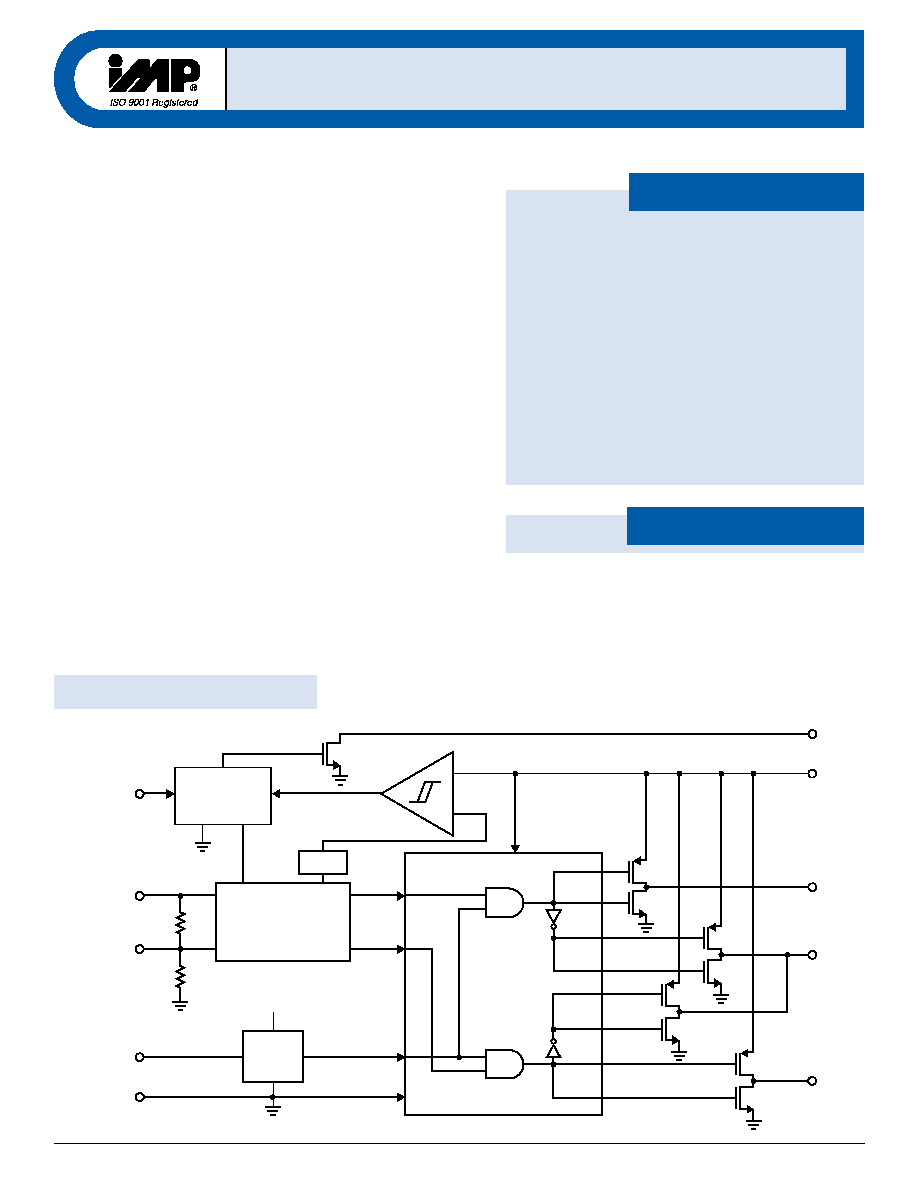
The IMP522 is a dual-output, high-voltage electroluminescent (EL) lamp
driver. Either or both EL lamp driver outputs can be turned ON with the
LMPSEL select pin. One EL lamp is connected between V
A
and V
AB
and
the other is connected between V
B
and V
AB
. V
AB
is a common pin for both
lamps. With an input supply voltage between 2.0V and 6.5V, the typical
regulated lamp drive voltage is 220V peak-to-peak.
The device uses a single inductor and a minimum number of passive
components: a storage capacitor, a fast recovery diode and two resistors
to set the PWM and EL drive frequencies. These can be independently
set to optimize brightness and minimize power consumption. R
SW
is
connected between the R
SW-OSC
pin and the supply pin V
DD
to set the
frequency for the internal 4.0
switching MOSFET. The switch duty cycle
is 88%. The EL lamp driver frequency is set by R
EL
connected between the
R
EL-OSC
pin and the V
DD
pin.
Designed to minimize battery current drain, the IMP522 draws 2mA maxi-
mum. A power-saving shutdown mode reduces current to 2µA maximum.
The IMP522 is available in a compact 10-pin MicroSO package and in die form.
Block Diagram

I M P 5 2 2
I M P 5 2 2
2
408-432-9100/www.impweb.com
© 2001 IMP, Inc.
Parameter
Symbol
Conditions
Min
Typ
Max
Units
ON-resistance of MOS Switch
R
DS(ON)
I = 100mA
4.0
8.0
Output Voltage Regulation
V
CS
V
DD
= 2.0 to 6.5V,
110
120
V
T = ≠40∞C to 85∞C
Output Voltage Peak-to-Peak (in regulation)
V
A
-V
AB,
V
B
-V
AB
In Regulation
220
V
Input Current at V
DD
Pin
I
DD
LMPSEL = GND
650
µA
Powerdown Input Current
I
DDQ
V
RSW≠OSC
< 100mA
2
µA
V
DD
= 2.0 to 6.5
T = ≠40∞C to 85∞C
Input Crrent Plus Inductor Current
I
IN
See Figure 1
30
mA
LMPSEL = GND or V
DD
LMPSEL = floating
43
mA
Output Drive Frequency
f
EL
See Figure 1
250
Hz
Switching Frequency
f
SW
See Figure 1
61
kHz
Switching Duty Cycle
D
SW
See Figure 1
88
%
LMPSEL Low-Level Threshold
V
IL
0.3 V
DD
V
LMPSEL High-Level Threshold
V
IH
0.7 V
DD
V
LMPSEL Input Resistance
R
LMPSEL
50
k
LMPSEL Sink/Source Resistance
I
LMPSEL
Floating/Hign Impedance State
± 5
µA
LMPSEL Hysteresis
V
hys
50
mV
4
L
X
3
C
S
2
R
SW-OSC
1
V
DD
7
LMPSEL
5
V
B
6
GND
8
V
AB
9
V
A
10 R
EL-OSC
522_02.eps
IMP522
MicroSO
Part Number
Input Voltage
Temperature Range
Pins-Package
IMP522EMB
2.0V to 6.5V
≠ 40∞C to +85∞C
10-MicroSO
V
DD
, R
SW-OSC
and R
EL-OSC
. . . . . . . . . . . . . . . . . ≠0.5V to +7.0V
C
S
, L
X
. . . . . . . . . . . . . . . . . . . . . . . . . . . . . . . . . ≠0.5V to +120V
Operating Temperature Range . . . . . . . . . . . . ≠40∞C to +85∞C
Storage Temperature Range . . . . . . . . . . . . . . ≠65∞C to +150∞C
Power Dissipation (MicroSO) . . . . . . . . . . . . . 500mW
V
A
, V
B,
V
AB
. . . . . . . . . . . . . . . . . . . . . . . . . . . . . ≠0.5V to V
CS
(pin 3)
Unless otherwise noted, V
DD
= 3.0V, R
SW
= 910k
, R
EL
= 2.7M
, L = 220µH and T
A
= 25∞C.
Note: All voltages are referenced to GND.
These are stress ratings only and functional operation is not
implied. Exposure to absolute maximum ratings for prolonged
time periods may affect device reliability.
Add /T to ordering part number for Tape and Reel.
Ordering Information
Pin Configuration
Absolute Maximum Ratings
Electrical Characteristics

I M P 5 2 2
I M P 5 2 2
© 2001 IMP, Inc.
Electroluminescent Lamp Drivers
3
Pin Descriptions
r
e
b
m
u
N
n
i
P
e
m
a
N
n
o
i
t
c
n
u
F
1
V
D
D
d
e
t
a
l
u
g
e
r
n
u
e
t
a
r
a
p
e
s
a
o
t
r
o
e
r
e
h
d
e
t
c
e
n
n
o
c
e
b
y
a
m
L
r
o
t
c
u
d
n
I
.
y
l
p
p
u
s
e
g
a
t
l
o
v
e
v
i
t
i
s
o
P
.
y
l
p
p
u
s
2
R
C
S
O
-
W
S
R
r
o
t
s
i
s
e
r
l
a
n
r
e
t
x
e
e
h
T
.
n
i
p
r
o
t
s
i
s
e
r
e
d
o
m
-
h
c
t
i
w
S
W
S
.
y
c
n
e
u
q
e
r
f
g
n
i
h
c
t
i
w
s
s
e
n
i
m
r
e
t
e
d
3
C
S
l
a
u
q
e
y
l
e
t
a
m
i
x
o
r
p
p
a
s
i
p
m
a
l
L
E
e
h
t
s
s
o
r
c
a
e
g
a
t
l
o
v
e
h
T
.
r
o
t
i
c
a
p
a
c
e
g
a
r
o
t
s
r
e
t
r
e
v
n
o
c
t
s
o
o
B
C
t
a
e
g
a
t
l
o
v
e
h
t
e
c
i
w
t
o
t
S
.
4
L
X
.
L
r
o
t
c
u
d
n
i
k
c
a
b
y
l
f
o
t
n
o
i
t
c
e
n
n
o
C
5
V
B
.
B
p
m
a
L
L
E
r
o
f
t
u
p
t
u
O
6
D
N
G
.
d
n
u
o
r
G
7
V
B
A
.
s
p
m
a
l
L
E
h
t
o
b
r
o
f
l
a
n
i
m
r
e
t
n
o
m
m
o
C
8
V
A
.
A
p
m
a
L
L
E
r
o
f
t
u
p
t
u
O
9
L
E
S
P
M
L
.
s
p
m
a
l
h
t
o
b
r
o
B
p
m
a
l
r
o
A
p
m
a
l
r
e
h
t
i
e
t
c
e
l
e
S
.
n
i
p
t
u
p
n
i
e
t
a
t
s
-
e
e
r
h
t
l
a
t
i
g
i
D
0
1
R
C
S
O
-
L
E
R
r
o
t
s
i
s
e
r
l
a
n
r
e
t
x
E
.
n
i
p
g
n
i
t
t
e
s
y
c
n
e
u
q
e
r
f
r
o
t
a
ll
i
c
s
o
p
m
a
l
L
E
e
h
T
L
E
V
o
t
d
e
t
c
e
n
n
o
c
D
D
s
t
e
s
.
s
p
m
a
l
h
t
o
b
r
o
f
y
c
n
e
u
q
e
r
f
e
v
i
r
d
p
m
a
L
L
E
e
h
t
s
p
e
.
1
0
t
_
2
2
5
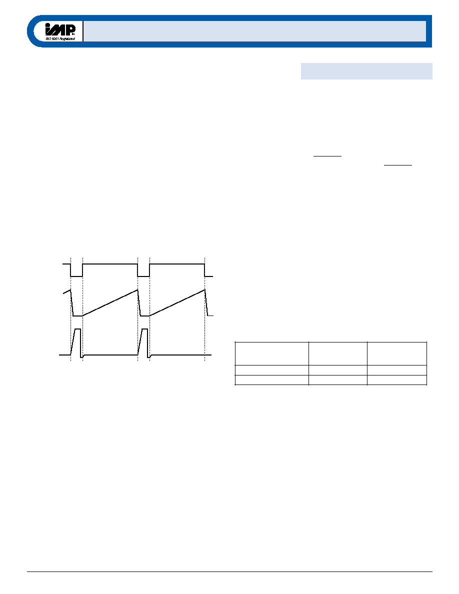
Figure 1. Test Circuit
Application Information
+
≠
+
V
DD
R
SW-OSC
C
S
L
X
R
EL-OSC
V
A
V
AB
LMPSEL
V
B
GND
10
9
8
7
EL LAMP
10nF
EL LAMP
10nF
1
2
3
4
6
5
IMP522
R
EL
Enable/Disable Strobe
V
DD
FDLL400
L
522_04.eps
ON = V
DD
OFF = 0V
R
SW
C
S
0.1
µF
10
µF
L = 220
µH
R
EL
= 2.7M
R
SW
= 910k

I M P 5 2 2
I M P 5 2 2
4
408-432-9100/www.impweb.com
© 2001 IMP, Inc.
Application Information
EL Lamp Drive
The outputs V
A
≠ V
AB
and V
B
≠ V
AB
are configured as H-bridges,
driven by the EL oscillator. Each output is switched between C
S
and ground on alternate phases, creating peak-to-peak signals
across the EL lamps of twice the regulated voltage.
EL Lamp Selection: LMPSEL
The digital input pin LMPSEL allows either or both EL lamps to
be active. Lamp A is active when LMPSEL is LOW and lamp B is
active when LMPSEL is HIGH. When LMPSEL is left floating or
driven by a three-state driver in the high impedance state, both
lamp driver outputs are active.
The logic HIGH signal level is defined as greater than 0.7V
DD
and
logic LOW is defined as less than 0.3V
DD
. A floating level is rec-
ognized with the signal level between 0.3V
DD
and 0.7V
DD
, or
when the output impedance of the driving voltage signal source
is infinite (driver in OFF state).
Both drivers are OFF if the IMP522 is disabled.
L
E
S
P
M
L
l
a
n
g
i
S
e
v
i
r
D
A
p
m
a
L
V
A
d
n
a
V
B
A
e
v
i
r
D
B
p
m
a
L
V
B
d
n
a
V
B
A
H
G
I
H
F
F
O
N
O
W
O
L
N
O
F
F
O
/
g
n
i
t
a
o
l
F
e
c
n
a
d
e
p
m
I
h
g
i
H
N
O
N
O
s
p
e
.
2
0
t
_
2
2
5
EL Driver Output Overvoltage Regulator
The IMP522 maximum V
CS
output voltage is between 110V and
120V. The internal overvoltage regulator skips the inductor
switching whenever the voltage on the C
S
pin exceeds the regula-
tion threshold. The internal overvoltage detection trip point has a
hysterisis of 1V and a range of 110V to 120V at room temperature.
PWM Circuit Switching
The switching MOSFET is driven by the PWM signal (nominally
61kHz). During the first 88% of the period, the switch is ON,
providing a low impedance path (<8
) from L
X
to ground. This
causes the external inductor to charge. In the last 12% of the
period, the MOSFET is turned OFF. This causes the voltage on
the output of L
X
to rise up to a high value. At some point, this will
forward-bias the external diode, thus pumping charge into the
storage capacitor C
S
. The voltage on C
S
increases each cycle to
between 110V and 120V. When the internal regulation trip-point is
reached, the overvoltage regulator turns the MOSFET switch OFF
to conserve power.
I M P 5 2 2
I M P 5 2 2
© 2001 IMP, Inc.
Electroluminescent Lamp Drivers
5
Power Sequencing
To power up the chip, the R
SW-OSC
pin is connected to V
DD
through
the external R
SW
resistor. The voltage on the pin will charge up to
V
DD
/2. An internal threshold detector circuit monitors the pin
voltage and when it exceeds the threshold range (0.2V to 0.9V) it
powers up the oscillator and internal bias modules. This starts a
delay counter which is one half of the EL oscillator period, after
which power to the high voltage internal modules is applied. The
IMP522 is then operating fully.
To power down the chip, R
SW
is driven to ground via a switch or
logic gate. When the voltage on the driver side of the resistor falls
below V
DD
/2, there will be no input bias current into the R
SW-OSC
pin. This immediately powers down the internal high-voltage
circuits, which effectively shuts the lamp off. At this point the
oscillator and bias modules still draw quiescent current, but oscil-
lations have ceased. As the R
SW-OSC
pin voltage falls below 0.1, the
oscillator and bias modules are also fully powered down.
Figure 1. Driver Waveforms
522_03.eps
IN (Pulse)
I
LX
V
LX
Power Saving Disable Mode
The IMP522 can be powered up and down with R
SW-OSC
. In
normal operation, this resistor on the R
SW-OSC
pin is connected to
V
DD
or another voltage source. To power down (disable) the
IMP522, R
SW
is connected to ground.
When disabled, the IMP522 quiescent current drops to typically 20nA.
In die form, an extra pin ENABLE is available (contact factory).
Connecting this pad to V
DD
disables the chip. The ENABLE signal
can be driven by a microcontroller.
Oscillator Frequency Adjustment
The EL lamp drive and PWM boost converter oscillation frequen-
cies can be programmed independently.
The R
SW
resistor, connected between the R
SW-OSC
pin and V
DD
,
determines the Inductor Switching (or PWM-) frequency. For the
recommended nominal resistor value of 910k
, the frequency is
61kHz. For other resistor values, the frequency is inversely pro-
portional to the resistor value. Increasing the resistance will lower
the frequency.
The R
EL
resistor, connected between the R
EL-OSC
pin and V
DD
,
determines the EL lamp drive frequency. For the recommended
nominal resistor value of 2.7M
, the frequency is 250Hz. For
other resistor values, the frequency is inversely proportional to
the resistor value: increasing the resistance will lower the fre-
quency.
r
o
t
a
ll
i
c
s
O
l
a
n
i
m
o
N
r
o
t
s
i
s
e
R
l
a
n
i
m
o
N
y
c
n
e
u
q
e
r
F
e
v
i
r
D
p
m
a
L
L
E
R
L
E
M
7
.
2
=
z
H
0
5
2
)
M
W
P
(
h
c
t
i
w
S
r
o
t
c
u
d
n
I
R
W
S
k
0
1
9
=
z
H
k
1
6
s
p
e
.
3
0
t
_
2
2
5
Application Information