 | –≠–ª–µ–∫—Ç—Ä–æ–Ω–Ω—ã–π –∫–æ–º–ø–æ–Ω–µ–Ω—Ç: IMP560/D | –°–∫–∞—á–∞—Ç—å:  PDF PDF  ZIP ZIP |

© 2000 IMP, Inc.
408-432-9100/www.impweb.com
1
IMP560
IMP560
P
OWER
M
ANAGEMENT
P
P
o
o
w
w
er Ef
er Ef
f
f
icient
icient
EL Lam
EL Lam
p Dr
p Dr
iv
iv
er
er
N Night lights
N Automotive displays
N Cellular phones
N Pagers
N Clocks and radios
N Portable GPS receivers
N LCD module backlights
N 112V peak-to-peak typical AC output voltage
N Low input current (w/inductor current)......12mA
N Low disabled input current......50nA
N Wide operating voltage range - from 2.0V to 6.5V
N Simple design requires few passive components
N Adjustable output lamp frequency controls lamp
color and power consumption
N Adjustable converter frequency for minimum
power consumption
N IMP803 pin-compatible
N MicroSO package option
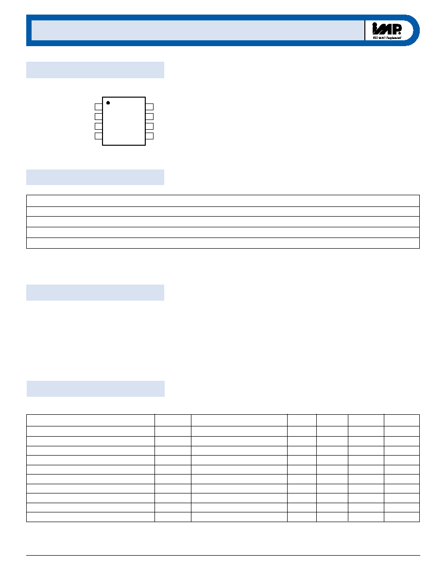
Block Diagram
≠
+
560_01.eps
V
DD
1
L
X
4
C
S
3
V
A
7
V
B
6
R
SW-OSC
2
Switch
Oscillator
Regulation
Control
IMP560
Bridge Output
Driver and
OSC
Q
Q
Q
V
REF
C
GND
5
R
EL-OSC
8
Q
The IMP560 is an Electroluminescent (EL) lamp driver designed for sys-
tems with low EL lamp drive voltage requirements. It is ideal for low
ambient light applications or where small lamps are used. With just one-
half the inductor current of the IMP803, the IMP560 reduces system
power consumption and extends battery life. Input supply voltage range
is 2.0V to 6.5V and quiescent current is a low 420
µA. Typical EL lamp
drive voltage is ±56V.
All four EL lamp-driving functions are on-chip. These are the switch-
mode power supply, its high-frequency oscillator, the high-voltage
H-bridge lamp driver and its low-frequency oscillator. EL lamps of up to
6nF capacitance can be driven to high brightness.
The circuit requires few external components; a single inductor, a single
diode, two capacitors and three resistors. Two of these resistors set the
frequencies for two internal oscillators. An internal circuit shuts down
the switching regulator when the lamp drive voltage exceeds 120V
peak-to-peak. This conserves power and extends battery life.
A disable mode puts the chip into a low current drain mode. With a 3.0V
supply, quiescent current drops to 200nA maximum, 50nA typical. The
chip is disabled by connecting the oscillator frequency setting resistor
R
SW
to ground.
The IMP560 is available in MicroSO and SO-8 packages and in die or
wafer form.
Key Features
Applications
I M P 5 6 0
I M P 5 6 0
2
408-432-9100/www.impweb.com
© 2000 IMP, Inc.
Parameter
Symbol
Conditions
Min
Typ
Max
Units
ON-resistance of MOS Switch
R
DS(ON)
I = 100mA
3.5
8
Output Voltage Regulation
V
CS
V
DD
= 2.0 to 6.5V
52
56
65
V
Output Voltage Peak-to-peak (in regulation)
V
A
-V
B
V
DD
= 2.0 to 6.5V
104
112
120
V
Quiescent V
DD
Supply Current, Disabled
I
DDIS
V
RSW-OSC
< 100mV
50
200
nA
Input Current at V
DD
Pin
I
DD
V
DD
= 3.0V, See Figure 1
470
700
µA
Input Current at V
DD
Pin
I
DD
V
DD
= 5.0V, See Figure 2
500
750
µA
Input Current: I
DD
Plus Inductor Current
I
IN
V
DD
= 3.0V, See Figure 1
12
mA
V
A-B
Output Drive Frequency
f
EL
V
DD
= 3.0V, See Figure 1
300
370
430
Hz
Switching Frequency
f
SW
V
DD
= 3.0V, See Figure 1
50
70
90
kHz
Switching Duty Cycle
D
SW
V
DD
= 3.0V, See Figure 1
88
%
Ordering Information
Pin Configuration
4
L
X
3
C
S
2
R
SW-OSC
1
V
DD
5
GND
6
V
B
7
V
A
8
R
EL-OSC
560_02.eps
IMP560
SO/MicroSO
Part Number
Input Voltage
Regulated Output Voltage
Temperature Range
Pins-Package
IMP560EMA
2.0V to 6.5V
YES
≠ 40
∞C to +85∞C
8-MicroSO
IMP560ESA
2.0V to 6.5V
YES
≠ 40
∞C to +85∞C
8-SO
IMP560/D*
2.0V to 6.5V
YES
25
∞C
Dice
IMP560/D1**
2.0V to 6.5V
YES
25
∞C
Dice
Absolute Maximum Ratings
Supply Voltage, V
DD
, V
RSW-OSC
and V
REL-OSC
. . . ≠0.5V to +7.0V
Output Voltage, V
CS
. . . . . . . . . . . . . . . . . . . . . . ≠0.5V to +120V
Operating Temperature Range . . . . . . . . . . . . . ≠40∞C to +85∞C
Storage Temperature Range. . . . . . . . . . . . . . . . ≠65∞C to +150∞C
Power Dissipation (SO) . . . . . . . . . . . . . . . . . . . 400mW
Power Dissipation (MicroSO) . . . . . . . . . . . . . . 300mW
Electrical Characteristics
Unless otherwise noted, V
DD
= 3.0V, R
SW
= 750k
, R
EL
= 2.0M
, and T
A
= 25∞C.
Note: All voltages are referenced to GND.
These are stress ratings only and functional operation is not
implied. Exposure to absolute maximum ratings for prolonged
time periods may affect device reliability.
Pin Compatible With IMP803
* Disable pad not active
** Disable pad active
I M P 5 6 0
I M P 5 6 0
© 2000 IMP, Inc.
Electroluminescent Lamp Driver
3
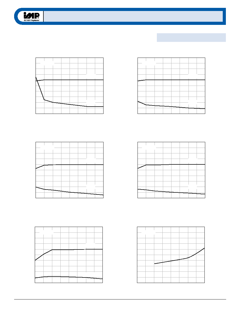
2.0
V
CS
(V), I
IN
(mA)
V
IN
(V)
100
80
60
40
20
0
V
CS
, I
IN
vs. V
IN
3.0
4.0
5.0
6.0
650_03.eps
L = 100
µH
V
CS
I
IN
2.0
V
CS
(V), I
IN
(mA)
V
IN
(V)
100
80
60
40
20
0
V
CS
, I
IN
vs. V
IN
3.0
4.0
5.0
6.0
650_06.eps
L = 330
µH
V
CS
I
IN
2.0
V
CS
(V), I
IN
(mA)
V
IN
(V)
100
80
60
40
20
0
V
CS
, I
IN
vs. V
IN
3.0
4.0
5.0
6.0
650_07.eps
L = 560
µH
V
CS
I
IN
2.0
V
CS
(V), I
IN
(mA)
V
IN
(V)
100
80
60
40
20
0
V
CS
, I
IN
vs. V
IN
3.0
4.0
5.0
6.0
650_04.eps
L = 470
µH
V
CS
I
IN
2.0
V
CS
(V), I
IN
(mA)
V
IN
(V)
100
80
60
40
20
0
V
CS
, I
IN
vs. V
IN
3.0
4.0
5.0
6.0
650_05.eps
L = 1mH
V
CS
I
IN
Typical Characteristics
2.0
I
DD
(
µ
A)
V
DD
(V)
800
700
600
500
400
300
I
DD
vs. V
DD
3.0
4.0
5.0
6.0
650_8.eps
L = 560
µH

I M P 5 6 0
I M P 5 6 0
4
408-432-9100/www.impweb.com
© 2000 IMP, Inc.
Pin Descriptions
External Components
High≠Voltages Present
Pin Number
Name
Function
1
V
DD
Positive voltage supply for the IMP560. Inductor L may be connected here or to a
separate unregulated supply.
2
R
SW-OSC
Switch-mode resistor pin. Switching frequency is determined by an external resistor, R
SW
.
3
C
S
Boost converter storage capacitor. The voltage across the EL lamp is equal to twice the
voltage at C
S
.
4
L
X
Connection to flyback inductance, L.
5
GND
Ground pin.
6
V
B
EL lamp drive. The lamp is connected in a high-voltage bridge circuit with V
B
providing
the complementary connection to V
A
. The peak-to-peak AC voltage across the EL lamp is
thus two times V
CS
.
7
V
A
EL lamp drive. (See above)
8
R
EL-OSC
The EL lamp oscillator frequency setting pin. The oscillator frequency is controlled
by external resistor R
EL
.
External Component
Description and Selection Guide
Diode
A fast reverse recovery diode, with BV > 100, such as a 1N4148.
Capacitor C
S
This is the high voltage capacitor that stores the inductive energy transferred through the
diode. A 100 volt capacitor between 10nF and 100nF is recommended.
Resistor R
EL
The EL lamp oscillator frequency setting resistor. This resistor, connected between the
R
EL-OSC
pin and ground, provides an oscillator frequency inversely proportional to R
EL
;
as R
EL
increases, the EL lamp frequency decreases along with the current drawn by the lamp.
Lamp color is also determined by this frequency. A 2M
resistor between the R
EL-OSC
pin and the
V
DD
supply results in a lamp frequency around 350Hz: a 1M
resistor will give 700Hz.
Resistor R
SW
Switching Oscillator frequency setting resistor. The switching oscillator resistor is connected
between the R
SW-OSC
pin and the V
DD
supply. The switching frequency is inversely proportional
to the resistor value, dropping as the resistance increases.
Inductor L
The inductor provides the voltage boost needed by means of inductive "flyback". The internal
MOSFET switch alternately opens and closes the ground connection for the inductor at the
L
X
pin. When this internal switch opens, the inductor potential will forward-bias the diode
and the current will pass through the storage capacitor C
S
, charging it to a high voltage.
Smaller inductors are preferred to prevent saturation. As the value of the inductor
increases (and the series DC resistance of the inductor decreases), the switching frequency
set by R
SW
should be increased to prevent saturation. In general, smaller value inductors that
can handle more current are more desirable when larger area EL lamps must be driven.
The IMP560 generates high voltages and caution should
be exercised.
I M P 5 6 0
I M P 5 6 0
© 2000 IMP, Inc.
Electroluminescent Lamp Driver
5
+
≠
V
DD
R
SW-OSC
C
S
L
X
R
EL-OSC
V
A
V
B
GND
8
7
6
5
1
2
3
4
IMP560
2M
750k
560
µH
1
V
IN
= 3.0V
0.1
µF
2
L
1N4148
10nF
Equivalent to
3 in
2
lamp
Note:
1. Murata part # LQH4N561K04 (DC resistance <14.5
)
2. Larger values may be required depending upon supply impedance.
560_09.eps
0.1
µF
100V
ON = V
DD
OFF = 0V
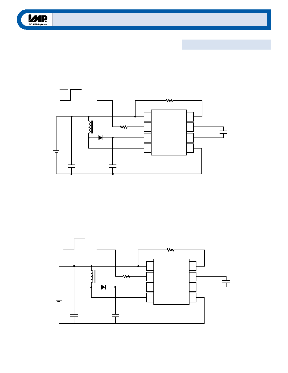
Figure 1. 3.0V Application
Test and Application Circuit, 3.0V
Figure 1 shows the IMP560 configured to drive a 3-square-inch
EL lamp, represented as a 10nF capacitor.
+
≠
ON = V
DD
OFF = 0V
V
DD
R
SW-OSC
C
S
L
X
R
EL-OSC
V
A
V
B
GND
8
7
6
5
1
2
3
4
IMP560
2M
750k
560
µH
1
V
IN
= 5.0V
0.1
µF
2
L
1N4148
6 in
2
lamp
Note:
1. Murata part # LQH4N561K04 (DC resistance <14.5
)
2. Larger values may be required depending upon supply impedance.
560_10.eps
0.1
µF
100V
Figure 2. 5.0V Application
Test and Application Circuit, 5.0V
Figure 2 shows a 5.0V input application driving a 6-square-inch
EL lamp.
Application Information

I M P 5 6 0
I M P 5 6 0
6
408-432-9100/www.impweb.com
© 2000 IMP, Inc.
Enable/Disable Operation
Figure 3 shows the IMP560 can be enabled via a logic gate that con-
nects R
SW
to V
DD
, and disabled by connecting it to ground. R
EL
may
be connected either to V
DD
or to the gate.
R
SW
Connection
IMP560 State
V
DD
Enabled
Ground
Disabled
Figure 3. Enable/Disable Operation
+
≠
ON = V
DD
OFF = 0V
V
DD
R
SW-OSC
C
S
L
X
R
EL-OSC
V
A
V
B
GND
8
7
6
5
1
2
3
4
IMP560
R
EL
CMOS
Gate
R
SW
L
1
V
IN
0.1
µF
2
15V
1N4148
EL lamp
Note:
1. Murata part # LQH4N561K04 (DC resistance <14.5
)
2. Larger values may be required depending upon supply impedance.
560_11.eps
0.1
µF
100V
Enable/Disable Table
Dual Supply Operation with 1.5V Battery
The IMP560 can also be operate from a single battery cell when a
regulated voltage higher than 2.0V is also available. The dual
supply configuration, shown in Figure 4, uses the regulated
voltage to operate the IMP560 while the energy for the high-
voltage boost circuit comes from the battery. The current to run
the internal logic is typically 420
µA.
The circuit of Figure 4 can also be used with batteries that exceed
6.0V as long as V
DD
does not exceed 6.5V.
+
≠
V
DD
R
SW-OSC
C
S
L
X
R
EL-OSC
V
A
V
B
GND
8
7
6
5
1
2
3
4
IMP560
R
EL
Regulated Voltage
(2.0V to 6.5V)
R
SW
L
Battery
Voltage
V
IN
0.1
µF
*
1N4148
EL lamp
560_12.eps
0.1
µF
100V
C
S
* Larger values may be required
depending upon supply impedance
ON = V
DD
OFF = 0V
Figure 4. Dual Supply Operation with High Battery Voltages
I M P 5 6 0
I M P 5 6 0
© 2000 IMP, Inc.
Electroluminescent Lamp Driver
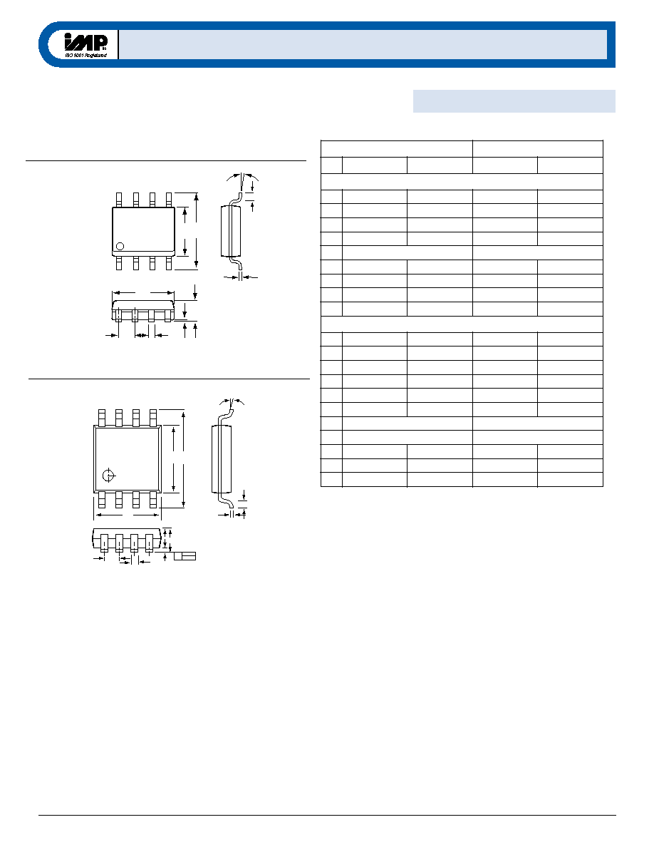
7
L
0
∞≠ 8∞
C
H
E
N
e
D
B
A1
A
SO (8-Pin).eps
SO (8-Pin)
MicroSO (8-Pin)
e
b
D
E1 E
a
L
+
C
D
0.10mm
0.004in
A1
A2
A
MicroSO (8-Pin).eps
s
e
h
c
n
I
s
r
e
t
e
m
i
l
l
i
M
n
i
M
x
a
M
n
i
M
x
a
M
*
)
n
i
P
-
8
(
O
S
A
3
5
0
.
0
9
6
0
.
0
5
3
.
1
5
7
.
1
1
A
4
0
0
.
0
0
1
0
.
0
0
1
.
0
5
2
.
0
B
3
1
0
.
0
0
2
0
.
0
3
3
.
0
1
5
.
0
C
7
0
0
.
0
0
1
0
.
0
9
1
.
0
5
2
.
0
e
0
5
0
.
0
7
2
.
1
E
0
5
1
.
0
7
5
1
.
0
0
8
.
3
0
0
.
4
H
8
2
2
.
0
4
4
2
.
0
0
8
.
5
0
2
.
6
L
6
1
0
.
0
0
5
0
.
0
0
4
.
0
7
2
.
1
D
9
8
1
.
0
7
9
1
.
0
0
8
.
4
0
0
.
2
*
*
)
n
i
P
-
8
(
O
S
o
r
c
i
M
A
≠
≠
≠
≠
≠
3
3
4
0
.
0
≠
≠
≠
≠
0
1
.
1
1
A
0
2
0
0
.
0
9
5
0
0
.
0
0
5
0
.
0
5
1
.
0
2
A
5
9
2
0
.
0
4
7
3
0
.
0
5
7
.
0
5
9
.
0
b
8
9
0
0
.
0
7
5
1
0
.
0
5
2
.
0
0
4
.
0
C
1
5
0
0
.
0
1
9
0
0
.
0
3
1
.
0
3
2
.
0
D
2
4
1
1
.
0
0
2
2
1
.
0
0
9
.
2
0
1
.
3
e
C
S
B
6
5
2
0
.
0
C
S
B
5
6
.
0
E
C
S
B
3
9
1
.
0
C
S
B
0
9
.
4
1
E
2
4
1
1
.
0
0
2
2
1
.
0
0
9
.
2
0
1
.
3
L
7
5
1
0
.
0
6
7
2
0
.
0
0
4
.
0
0
7
.
0
a
∞
0
∞
6
∞
0
∞
6
A
A
2
1
0
-
S
M
g
n
i
w
a
r
D
C
E
D
E
J
*
A
A
7
8
1
-
O
M
g
n
i
w
a
r
D
C
E
D
E
J
*
*
3
t
a
.
1
0
t
_
3
0
8
Package Dimensions

IMP, Inc.
Corporate Headquarters
2830 N. First Street
San Jose, CA 95134-2071
Tel: 408-432-9100
Fax: 408-434-0335
e-mail: info@impinc.com
http://www.impweb.com
The IMP logo is a registered trademark of IMP, Inc.
All other company and product names are trademarks of their respective owners.
© 2000 IMP, Inc.
Printed in USA
Publication #: 2005
Revision:
C
Issue Date:
09/01/00
Type:
Product
I M P 5 6 0
I M P 5 6 0