 | –≠–ª–µ–∫—Ç—Ä–æ–Ω–Ω—ã–π –∫–æ–º–ø–æ–Ω–µ–Ω—Ç: IMP706J | –°–∫–∞—á–∞—Ç—å:  PDF PDF  ZIP ZIP |
©
1999 IMP, Inc.
408-432-9100/www.impweb.com
1
Key Features
Applications
x
Computers and controllers
x
CTI applications
x
Embedded controllers
x
Battery operated systems
x
Intelligent instruments
x
Wireless communication systems
x
PDAs and handheld equipment
x
Lower power, pin compatible replacements for
Maxim MAX706P/R/S/T, MAX708R/S/T
≠ 30% lower supply current:140µA vs. 200µA
x
Precision power supply monitor
≠ 2.63V threshold (IMP706P/R, IMP708R)
≠ 2.93V threshold (IMP706S, IMP708S)
≠ 3.08V threshold (IMP706T, IMP708T)
≠ New 4.00V threshold (IMP706J, IMP708J)
x
Debounced manual reset input
x
Auxiliary voltage monitor comparator
≠ 1.25V threshold
≠ Battery monitor/auxiliary supply monitor
x
Watchdog timer (IMP706P/R/S/T/J)
≠ Watchdog can be disabled by floating WDI
x
200ms reset time delay
x
Three reset signal options
≠ Active HIGH: IMP706P
≠ Active LOW: IMP706R/S/T/J
≠ Active HIGH & LOW outputs: IMP708R/S/T/J
x
DIP, SO and MicroSO packages
x
Guaranteed RESET assertion to V
CC
= 1.1V
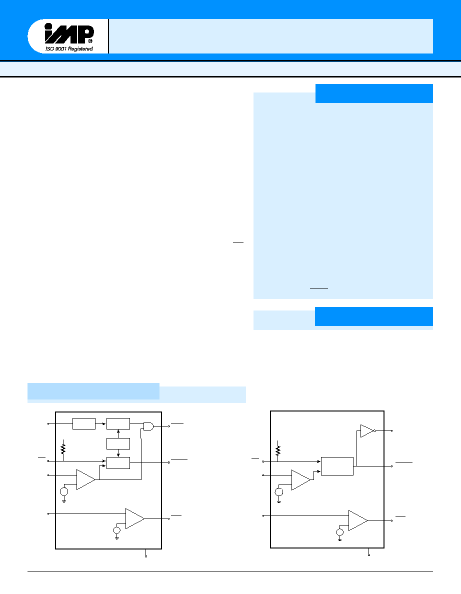
Block Diagrams
IMP706P/R/S/T/J, IMP708R/S/T/J
IMP706P/R/S/T/J, IMP708R/S/T/J
P
OWER
M
ANAGEMENT
3/3.3/4.0V
3/3.3/4.0V
µ
µ
P Super
P Super
visor Cir
visor Cir
cuits
cuits
≠ Lo
≠ Lo
w suppl
w suppl
y cur
y cur
r
r
ent
ent
≠ W
≠ W
atc
atc
hdog timer
hdog timer
≠ Br
≠ Br
o
o
wnout det
wnout det
ection
ection
The IMP706P/R/S/T/J and IMP708R/S/T/J CMOS supervisor circuits
monitor power-supply and battery voltage level, and
µ
P/
µ
C operation.
A reset is generated when the supply drops below 2.63V (IMP706P/R,
IMP708R), 2.93V (IMP706S, IMP708S), 3.08V (IMP706T, IMP708T) or 4.00
(IMP706J, IMP708J).
The family offers several functional options. Each device generates a
reset signal during power-up, power-down and during brownout
conditions.
In addition, the IMP706P/R/S/T/J feature a 1.6 second watchdog timer.
The watchdog timer output will trigger a reset if connected to MR.
Unlike competitive devices, floating the WDI input pin disables the
watchdog timer.
The IMP708R/S/T/J have both active-HIGH and active-LOW reset out-
puts but no watchdog function. The IMP706P has the same pin-out and
functions as the IMP706R but has an active-HIGH reset output.
A versatile power-fail circuit, useful in checking battery levels and
non-5V supplies, has a 1.25V threshold. All devices have a manual
reset input.
All devices are available in 8-pin DIP, SO and the compact MicroSO
packages. The MicroSO package requires 50% less PC board area than
the conventional SO package.
RESET
RESET
V
CC
RESET
Generator
2.63V (IMP708R)
2.93V (IMP708S)
3.08V (IMP708T)
4.00V (IMP708J)
V
CC
+
≠
+
MR
IMP708R/S/T/J
PFO
GND
1.25V
≠
+
PFI
706P_02.eps
20k
1.25V
≠
+
MR
WDI
IMP706P/R/S/T/J
WDO
RESET
(RESET) IMP706P
PFO
GND
V
CC
20k
RESET
Generator
2.63V (IMP706P/R)
2.93V (IMP706S)
3.08V (IMP706T)
4.00V (IMP706J)
V
CC
+
≠
+
PFI
Timebase
Watchdog
Timer
Transition
Detector
706P_01.eps

2
408-432-9100/www.impweb.com
©
1999 IMP, Inc.
Ordering Information
Pin Configuration
IMP706P/R/S/T/J, IMP708R/S/T/J
IMP706P/R/S/T/J, IMP708R/S/T/J
IMP708R/S/T/J
1
2
3
4
MR
V
CC
GND
PFI
RESET
RESET
NC
PFO
8
7
6
5
IMP706P
1
2
3
4
MR
V
CC
GND
PFI
WDO
RESET
WDI
PFO
8
7
6
5
IMP706R/S/T/J
1
2
3
4
MR
V
CC
GND
PFI
WDO
RESET
WDI
PFO
8
7
6
5
IMP706P
IMP706R/S/T/J
1
2
3
4
(RESET) RESET
(IMP706P)
WDO
MR
V
CC
WDI
PFO
PFI
GND
8
7
6
5
IMP708R/S/T/J
1
2
3
4
RESET
RESET
MR
V
CC
NC
PFO
PFI
GND
8
7
6
5
706P_03.eps
DIP/SO
MicroSO
Operating
Part Number
Package
Temperature Range Reset Threshold
Reset Polarity
Watchdog Timer
IMP706PCPA
8-Plastic DIP
0∞C to +70∞C
2.63
HIGH
YES
IMP706PCSA
8-SO
0∞C to +70∞C
2.63
HIGH
YES
IMP706PCUA
8-MicroSO
0∞C to +70∞C
2.63
HIGH
YES
IMP706PEPA
8-Plastic DIP
≠40∞C to +85∞C
2.63
HIGH
YES
IMP706PESA
8-SO
≠40∞C to +85∞C
2.63
HIGH
YES
IMP706RCPA
8-Plastic DIP
0∞C to +70∞C
2.63
LOW
YES
IMP706RCSA
8-SO
0∞C to +70∞C
2.63
LOW
YES
IMP706RCUA
8-MicroSO
0∞C to +70∞C
2.63
LOW
YES
IMP706REPA
8-Plastic DIP
≠40∞C to +85∞C
2.63
LOW
YES
IMP706RESA
8-SO
≠40∞C to +85∞C
2.63
LOW
YES
IMP706SCPA
8-Plastic DIP
0∞C to +70∞C
2.93
LOW
YES
IMP706SCSA
8-SO
0∞C to +70∞C
2.93
LOW
YES
IMP706SCUA
8-MicroSO
0∞C to +70∞C
2.93
LOW
YES
IMP706SEPA
8-Plastic DIP
≠40∞C to +85∞C
2.93
LOW
YES
IMP706SESA
8-SO
≠40∞C to +85∞C
2.93
LOW
YES
IMP706TCPA
8-Plastic DIP
0∞C to +70∞C
3.08
LOW
YES
IMP706TCSA
8-SO
0∞C to +70∞C
3.08
LOW
YES
IMP706TCUA
8-MicroSO
0∞C to +70∞C
3.08
LOW
YES
IMP706TEPA
8-Plastic DIP
≠40∞C to +85∞C
3.08
LOW
YES
IMP706TESA
8-SO
≠40∞C to +85∞C
3.08
LOW
YES
IMP706JCPA
8-Plastic DIP
0∞C to +70∞C
4.00
LOW
YES
IMP706JCSA
8-SO
0∞C to +70∞C
4.00
LOW
YES
IMP706JCUA
8-MicroSO
0∞C to +70∞C
4.00
LOW
YES
IMP706JEPA
8-Plastic DIP
≠40∞C to +85∞C
4.00
LOW
YES
IMP706JESA
8-SO
≠40∞C to +85∞C
4.00
LOW
YES
IMP708RCPA
8-Plastic DIP
0∞C to +70∞C
2.63
Dual: HIGH & LOW
NO
IMP708RCSA
8-SO
0∞C to +70∞C
2.63
Dual: HIGH & LOW
NO
IMP708RCUA
8-MicroSO
0∞C to +70∞C
2.63
Dual: HIGH & LOW
NO
IMP708REPA
8-Plastic DIP
≠40∞C to +85∞C
2.63
Dual: HIGH & LOW
NO
IMP708RESA
8-SO
≠40∞C to +85∞C
2.63
Dual: HIGH & LOW
NO
IMP708SCPA
8-Plastic DIP
0∞C to +70∞C
2.93
Dual: HIGH & LOW
NO
IMP708SCSA
8-SO
0∞C to +70∞C
2.93
Dual: HIGH & LOW
NO
IMP708SCUA
8-MicroSO
0∞C to +70∞C
2.93
Dual: HIGH & LOW
NO
IMP708SEPA
8-Plastic DIP
≠40∞C to +85∞C
2.93
Dual: HIGH & LOW
NO
IMP708SESA
8-SO
≠40∞C to +85∞C
2.93
Dual: HIGH & LOW
NO
IMP708TCPA
8-Plastic DIP
0∞C to +70∞C
3.08
Dual: HIGH & LOW
NO
IMP708TCSA
8-SO
0∞C to +70∞C
3.08
Dual: HIGH & LOW
NO
IMP708TCUA
8-MicroSO
0∞C to +70∞C
3.08
Dual: HIGH & LOW
NO
IMP708TEPA
8-Plastic DIP
≠40∞C to +85∞C
3.08
Dual: HIGH & LOW
NO
IMP708TESA
8-SO
≠40∞C to +85∞C
3.08
Dual: HIGH & LOW
NO
IMP708JCPA
8-Plastic DIP
0∞C to +70∞C
4.00
Dual: HIGH & LOW
NO
IMP708JCSA
8-SO
0∞C to +70∞C
4.00
Dual: HIGH & LOW
NO
IMP708JCUA
8-MicroSO
0∞C to +70∞C
4.00
Dual: HIGH & LOW
NO
IMP708JEPA
8-Plastic DIP
≠40∞C to +85∞C
4.00
Dual: HIGH & LOW
NO
IMP708JESA
8-SO
≠40∞C to +85∞C
4.00
Dual: HIGH & LOW
NO
©
1999 IMP, Inc.
408-432-9100/www.impweb.com
3
IMP706P/R/S/T/J, IMP708R/S/T/J
IMP706P/R/S/T/J, IMP708R/S/T/J
Absolute Maximum Ratings
Electrical Characteristics
Pin Terminal Voltage with Respect to Ground
V
CC
. . . . . . . . . . . . . . . . . . . . . . . . . . . . . . . . . ≠0.3V to 6.0V
All other inputs . . . . . . . . . . . . . . . . . . . . . . . . ≠0.3V to (V
CC
+ 0.3V)
Input Current at V
CC
and GND . . . . . . . . . . 20mA
Output Current: All outputs . . . . . . . . . . . . . 20mA
Rate of Rise at V
CC
. . . . . . . . . . . . . . . . . . . . . 100V/
µ
s
Plastic DIP Power Dissipation . . . . . . . . . . . 700mW
(Derate 9mW/
∞
C above 70
∞
C)
SO Power Dissipation . . . . . . . . . . . . . . . . . . 470mW
(Derate 5.9mW/
∞
C above 70
∞
C)
MicroSO Power Dissipation . . . . . . . . . . . . . 330mW
(Derate 4.1mW/
∞
C above 70
∞
C)
Operating Temperature Range
IMP706xE, IMP708xE . . . . . . . . . . . . . . . . . . ≠40
∞
C to +85
∞
C
IMP706xC, IMP708xC . . . . . . . . . . . . . . . . . . 0
∞
C to +70
∞
C
Storage Temperature Range . . . . . . . . . . . . . . ≠65
∞
C to +160
∞
C
Lead Temperature Soldering (10 sec) . . . . . . 300
∞
C
These are stress ratings only and functional operation is not implied.
Exposure to absolute maximum ratings for prolonged time periods may
affect device reliability.
Unless otherwise noted, specifications are over the operating temperature range and V
CC
supply voltages are 2.7V to 5.5V (IMP706P,
IMP708R), 3.0V to 5.5V (IMP706/8S), 3.15V to 5.5V (IMP706/8T) and 4.1V to 5.5V (IMP706/8J).
r
e
t
e
m
a
r
a
P
l
o
b
m
y
S
s
n
o
it
i
d
n
o
C
n
i
M
p
y
T
x
a
M
s
ti
n
U
e
g
a
t
l
o
V
g
n
i
t
a
r
e
p
O
e
g
n
a
R
V
C
C
C
x
8
0
7
P
M
I
,
C
x
6
0
7
P
M
I
E
x
8
0
7
P
M
I
,
E
x
6
0
7
P
M
I
1
.
1
2
.
1
5
.
5
5
.
5
V
t
n
e
r
r
u
C
y
l
p
p
u
S
V
C
C
V
6
.
3
<
I
C
C
V
=
R
M
,
E
x
6
0
7
P
M
I
,
C
x
6
0
7
P
M
I
C
C
g
n
i
t
a
o
l
F
I
D
W
,
5
7
0
4
1
µ
A
V
=
R
M
,
E
x
8
0
7
P
M
I
,
C
x
8
0
7
P
M
I
C
C
g
n
i
t
a
o
l
F
I
D
W
,
0
5
0
4
1
t
n
e
r
r
u
C
y
l
p
p
u
S
V
C
C
V
5
.
5
<
I
C
C
V
=
R
M
,
E
x
6
0
7
P
M
I
,
C
x
6
0
7
P
M
I
C
C
g
n
i
t
a
o
l
F
I
D
W
,
5
7
0
4
1
µ
A
V
=
R
M
,
E
x
8
0
7
P
M
I
,
C
x
8
0
7
P
M
I
C
C
g
n
i
t
a
o
l
F
I
D
W
,
0
5
0
4
1
d
l
o
h
s
e
r
h
T
T
E
S
E
R
V
T
R
s
e
c
i
v
e
d
R
d
n
a
P
s
e
c
i
v
e
d
S
s
e
c
i
v
e
d
T
s
e
c
i
v
e
d
J
5
5
.
2
5
8
.
2
0
0
.
3
9
8
.
3
3
6
.
2
3
9
.
2
8
0
.
3
0
0
.
4
0
7
.
2
0
0
.
3
5
1
.
3
0
1
.
4
V
d
l
o
h
s
e
r
h
T
T
E
S
E
R
s
i
s
e
r
e
t
s
y
H
0
4
V
m
h
t
d
i
W
e
s
l
u
P
T
E
S
E
R
t
S
R
V
C
C
,
)
s
e
c
i
v
e
d
R
/
P
,
8
/
6
0
7
P
M
I
(
V
3
=
V
C
C
)
s
e
c
i
v
e
d
T
/
S
,
8
/
6
0
7
P
M
I
(
V
3
.
3
=
V
C
C
)
s
e
c
i
v
e
d
J
,
8
/
6
0
7
P
M
I
(
V
4
.
4
=
0
4
1
0
0
2
0
8
2
s
m
V
C
C
V
5
=
0
0
2
h
t
d
i
W
e
s
l
u
P
R
M
t
R
M
V
<
V
5
.
4
C
C
V
5
.
5
<
0
5
1
s
n
V
<
V
6
.
3
C
C
)
s
e
c
i
v
e
d
J
8
/
6
0
7
P
M
I
(
V
5
.
4
<
V
)
X
A
M
(
T
S
R
V
<
C
C
)
s
e
c
i
v
e
d
T
/
S
/
R
/
P
8
/
6
0
7
P
M
I
(
V
6
.
3
<
0
0
5
y
a
l
e
D
t
u
O
T
E
S
E
R
o
t
R
M
t
D
M
V
<
V
6
.
3
C
C
)
s
e
c
i
v
e
d
J
8
/
6
0
7
P
M
I
(
V
5
.
4
<
V
)
X
A
M
(
T
S
R
V
<
C
C
)
s
e
c
i
v
e
d
T
/
S
/
R
/
P
8
/
6
0
7
P
M
I
(
V
6
.
3
<
0
5
7
s
n
V
<
V
5
.
4
C
C
V
5
.
5
<
0
5
2
d
l
o
h
s
e
r
h
T
t
u
p
n
I
R
M
V
H
I
V
)
X
A
M
(
T
S
R
V
<
C
C
V
5
.
4
<
V
7
.
0
C
C
V
V
L
I
V
)
X
A
M
(
T
S
R
V
<
C
C
V
5
.
4
<
6
.
0
V
H
I
V
<
V
5
.
4
C
C
V
5
.
5
<
0
.
2
V
L
I
V
<
V
5
.
4
C
C
V
5
.
5
<
8
.
0
r
o
t
s
i
s
e
R
p
u
-
ll
u
P
R
M
R
P
0
1
0
2
0
4
k
e
g
a
t
l
o
V
t
u
p
t
u
O
T
E
S
E
R
)
s
e
c
i
v
e
d
J
/
T
/
S
/
R
ll
A
(
V
H
O
I
E
C
R
U
O
S
0
0
8
=
µ
V
<
V
5
.
4
,
A
C
C
V
5
.
5
<
V
C
C
V
5
.
1
≠
V
V
L
O
I
K
N
I
S
V
<
V
5
.
4
,
A
m
2
.
3
=
C
C
V
5
.
5
<
4
.
0
V
H
O
I
E
C
R
U
O
S
0
0
5
=
µ
V
,
A
)
X
A
M
(
T
S
R
V
<
C
C
V
5
.
4
<
V
8
.
0
C
C
V
L
O
I
K
N
I
S
V
,
A
m
2
.
1
=
)
X
A
M
(
T
S
R
V
<
C
C
V
5
.
4
<
3
.
0
V
L
O
I
K
N
I
S
0
5
=
µ
V
,
A
C
C
)
s
e
c
i
v
e
d
C
x
8
0
7
P
M
I
,
C
x
6
0
7
P
M
I
(
V
1
.
1
=
3
.
0
I
K
N
I
S
0
0
1
=
µ
V
,
A
C
C
)
s
e
c
i
v
e
d
E
x
8
0
7
P
M
I
,
E
x
6
0
7
P
M
I
(
V
2
.
1
=
3
.
0

IMP706P/R/S/T/J, IMP708R/S/T/J
IMP706P/R/S/T/J, IMP708R/S/T/J
4
408-432-9100/www.impweb.com
©
1999 IMP, Inc.
Unless otherwise noted, specifications are over the operating temperature range and V
CC
supply voltages are 2.7V to 5.5V (IMP706P,
IMP708R), 3.0V to 5.5V (IMP706/8S), 3.15V to 5.5V (IMP706/8T) and 4.1V to 5.5V (IMP706/8J).
Electrical Characteristics
(cont.)
r
e
t
e
m
a
r
a
P
l
o
b
m
y
S
s
n
o
it
i
d
n
o
C
n
i
M
p
y
T
x
a
M
s
ti
n
U
e
g
a
t
l
o
V
t
u
p
t
u
O
T
E
S
E
R
P
6
0
7
P
M
I
V
H
O
I
E
C
R
U
O
S
0
0
8
=
µ
V
<
V
5
.
4
,
A
C
C
V
5
.
5
<
V
C
C
V
5
.
1
≠
V
V
L
O
I
K
N
I
S
V
<
V
5
.
4
,
A
m
2
.
3
=
C
C
V
5
.
5
<
4
.
0
V
H
O
I
E
C
R
U
O
S
0
0
5
=
µ
V
,
A
)
X
A
M
(
T
S
R
V
<
C
C
V
6
.
3
<
V
8
.
0
C
C
V
L
O
I
K
N
I
S
V
,
A
m
2
.
1
=
)
X
A
M
(
T
S
R
V
<
C
C
V
6
.
3
<
3
.
0
,
e
g
a
t
l
o
V
t
u
p
t
u
O
T
E
S
E
R
J
/
T
/
S
/
R
8
0
7
P
M
I
V
H
O
I
E
C
R
U
O
S
0
0
8
=
µ
V
<
V
5
.
4
,
A
C
C
V
5
.
5
<
V
C
C
V
5
.
1
≠
V
V
L
O
I
K
N
I
S
V
<
V
5
.
4
,
A
m
2
.
3
=
C
C
V
5
.
5
<
4
.
0
V
H
O
I
E
C
R
U
O
S
0
0
5
=
µ
V
,
A
)
X
A
M
(
T
S
R
V
<
C
C
V
5
.
4
<
V
8
.
0
C
C
V
L
O
I
K
N
I
S
V
,
A
m
2
.
1
=
)
X
A
M
(
T
S
R
V
<
C
C
V
5
.
4
<
3
.
0
d
o
i
r
e
P
t
u
o
e
m
i
T
g
o
d
h
c
t
a
W
t
D
W
V
C
C
)
s
e
c
i
v
e
d
R
/
P
,
6
0
7
P
M
I
(
V
3
=
V
C
C
)
s
e
c
i
v
e
d
T
/
S
,
6
0
7
P
M
I
(
V
3
.
3
=
V
C
C
)
s
e
c
i
v
e
d
J
,
6
0
7
P
M
I
(
V
4
.
4
=
0
.
1
6
.
1
5
2
.
2
s
h
t
d
i
W
e
s
l
u
P
I
D
W
t
P
W
V
L
I
V
,
V
4
.
0
=
H
I
V
8
.
0
=
C
C
V
,
)
X
A
M
(
T
S
R
V
<
C
C
V
5
.
4
<
0
0
1
s
n
h
t
d
i
W
e
s
l
u
P
I
D
W
t
P
W
V
L
I
V
,
V
4
.
0
=
H
I
V
8
.
0
=
C
C
V
<
V
5
.
4
,
C
C
V
5
.
5
<
0
5
s
n
d
l
o
h
s
e
r
h
T
t
u
p
n
I
I
D
W
V
H
I
V
C
C
V
5
=
5
.
3
V
V
L
I
8
.
0
V
H
I
V
)
X
A
M
(
T
S
R
V
<
C
C
V
5
.
4
<
V
7
.
0
C
C
V
L
I
6
.
0
t
n
e
r
r
u
C
t
u
p
n
I
I
D
W
V
=
I
D
W
C
C
y
l
n
O
6
0
7
P
M
I
,
0
5
0
5
1
µ
A
t
n
e
r
r
u
C
t
u
p
n
I
I
D
W
y
l
n
O
6
0
7
P
M
I
,
V
0
=
I
D
W
0
5
1
≠
0
5
≠
µ
A
e
g
a
t
l
o
V
t
u
p
t
u
O
O
D
W
V
H
O
I
E
C
R
U
O
S
0
0
8
=
µ
V
<
V
5
.
4
,
A
C
C
V
5
.
5
<
V
C
C
V
5
.
1
≠
V
V
L
O
I
K
N
I
S
V
<
V
5
.
4
,
A
m
2
.
1
=
C
C
V
5
.
5
<
4
.
0
V
H
O
I
E
C
R
U
O
S
0
0
5
=
µ
V
,
A
)
X
A
M
(
T
S
R
V
<
C
C
V
5
.
4
<
V
8
.
0
C
C
V
L
O
I
K
N
I
S
0
0
5
=
µ
V
,
A
)
X
A
M
(
T
S
R
V
<
C
C
V
5
.
4
<
3
.
0
d
l
o
h
s
e
r
h
T
t
u
p
n
I
I
F
P
V
s
e
c
i
v
e
d
R
/
P
r
o
F
.
g
n
il
l
a
f
I
F
P
C
C
T
/
S
r
o
F
.
V
3
=
V
s
e
c
i
v
e
d
C
C
V
s
e
c
i
v
e
d
J
r
o
F
.
V
3
.
3
=
C
C
.
V
4
.
4
=
2
.
1
5
2
.
1
3
.
1
V
t
n
e
r
r
u
C
t
u
p
n
I
I
F
P
5
2
≠
1
0
.
0
5
2
A
n
e
g
a
t
l
o
V
t
u
p
t
u
O
O
F
P
V
H
O
I
E
C
R
U
O
S
0
0
8
=
µ
V
<
V
5
.
4
,
A
C
C
V
5
.
5
<
V
C
C
V
5
.
1
≠
V
V
L
O
I
K
N
I
S
V
<
V
5
.
4
,
A
m
2
.
3
=
C
C
V
5
.
5
<
4
.
0
V
H
O
I
E
C
R
U
O
S
0
0
5
=
µ
V
,
A
)
X
A
M
(
S
R
V
<
C
C
V
5
.
4
<
V
8
.
0
C
C
V
L
O
I
K
N
I
S
V
,
A
m
2
.
1
=
)
X
A
M
(
S
R
V
<
C
C
V
5
.
4
<
3
.
0
Pin Number
IMP706P
IMP706R/S/T/J IMP708R/S/T/J
DIP/SO MicroSO DIP/SO MicroSO DIP/SO MicroSO Name
Function
Manual reset input. The active LOW input triggers
a reset pulse. It is pulled HIGH by a 20k
pull-up
1
3
1
3
1
3
MR
resistor. It is compatible with TTL/CMOS signals
when V
CC
= 5V. It can be shorted to ground
through a mechanical switch. Leave floating or
connect to V
CC
if the function is not used.
2
4
2
4
2
4
V
CC
Monitored power supply input.
3
5
3
5
3
5
GND
Ground
Power-fail input voltage monitor. With PFI less than
4
6
4
6
4
6
PFI
1.25V, PFO goes LOW. Connect PFI to ground
when not used.
Power-fail output. The output is active LOW and
5
7
5
7
5
7
PFO
sinks current when PFI is less than 1.25V. If not
used, leave the pin unconnected.
Watchdog input. WDI controls the internal watchdog
timer. A HIGH or LOW signal for 1.6 sec at WDI
allows the internal timer to run-out, setting WDO low.
6
8
6
8
--
--
WDI
A rising or falling edge must occur at WDI within
1.6 seconds or WDO goes LOW. The watchdog
function is disabled by floating WDI. The internal
watchdog timer clears when: RESET is asserted;
WDI is three-stated; or WDI sees a rising or falling edge.
--
--
--
--
6
8
NC
Not connected.
Active-LOW reset output. Pulses LOW for 200ms
when triggered, and stays LOW whenever V
CC
is
--
--
7
1
7
1
RESET
below the reset threshold. RESET remains LOW for
200ms after V
CC
rises above the RESET threshold
or MR goes from HIGH to LOW. A watchdog timeout
will not trigger RESET unless WDO is connected to MR.
Watchdog output. WDO goes LOW when the 1.6
second internal watchdog timer times-out and does
not go HIGH until a transition occurs at WDI. In
8
2
8
2
--
--
WDO
addition, when V
CC
falls below the reset threshold,
WDO goes LOW. Unlike RESET, WDO does not have
a minimum pulse width and as soon as V
CC
exceeds
the reset threshold, WDO becomes HIGH with no delay.
7
1
--
--
8
2
RESET
Active-HIGH reset output. RESET is the inverse of
RESET.
IMP706P/R/S/T/J, IMP708R/S/T/J
IMP706P/R/S/T/J, IMP708R/S/T/J
Pin Descriptions
Feature Summary
©
1999 IMP, Inc.
408-432-9100/www.impweb.com
5
IMP706P IMP706R IMP706S IMP706T IMP706J IMP708R IMP708S IMP708T IMP708J
Power-fail detector
s
s
s
s
s
s
s
s
s
Brownout detection
s
s
s
s
s
s
s
s
s
Debounced manual RESET input
s
s
s
s
s
s
s
s
s
Power-up/down RESET
s
s
s
s
s
s
s
s
s
Watchdog timer
s
s
s
s
s
Active-HIGH RESET
s
Active-LOW RESET
s
s
s
s
Active-LOW and HIGH RESETs
s
s
s
s
RESET threshold
2.63V
2.63V
2.93V
3.08V
4.00V
2.63V
2.93V
3.08V
4.00V