
©
1999 IMP, Inc.
408-432-9100/www.impweb.com
1
Key Features
Applications
N Computers and controllers
N CTI applications
N Embedded controllers
N Battery operated systems
N Intelligent instruments
N Wireless communication systems
N PDAs and handheld equipment
N Lower power, pin compatible replacements for
Maxim MAX706P/R/S/T, MAX708R/S/T
≠ 30% lower supply current:140µA vs. 200µA
N Precision power supply monitor
≠ 2.63V threshold (IMP706P/R, IMP708R)
≠ 2.93V threshold (IMP706S, IMP708S)
≠ 3.08V threshold (IMP706T, IMP708T)
≠ New 4.00V threshold (IMP706J, IMP708J)
N Debounced manual reset input
N Auxiliary voltage monitor comparator
≠ 1.25V threshold
≠ Battery monitor/auxiliary supply monitor
N Watchdog timer (IMP706P/R/S/T/J)
≠ Watchdog can be disabled by floating WDI
N 200ms reset time delay
N Three reset signal options
≠ Active HIGH: IMP706P
≠ Active LOW: IMP706R/S/T/J
≠ Active HIGH & LOW outputs: IMP708R/S/T/J
N DIP, SO and MicroSO packages
N Guaranteed RESET assertion to V
CC
= 1.1V
Block Diagrams
IMP706P/R/S/T/J, IMP708R/S/T/J
IMP706P/R/S/T/J, IMP708R/S/T/J
P
OWER
M
ANAGEMENT
3/3.3/4.0V
3/3.3/4.0V
µ
µ
P Super
P Super
visor Cir
visor Cir
cuits
cuits
≠ Lo
≠ Lo
w suppl
w suppl
y cur
y cur
r
r
ent
ent
≠ W
≠ W
atc
atc
hdog timer
hdog timer
≠ Br
≠ Br
o
o
wnout det
wnout det
ection
ection
The IMP706P/R/S/T/J and IMP708R/S/T/J CMOS supervisor circuits
monitor power-supply and battery voltage level, and
µP/µC operation.
A reset is generated when the supply drops below 2.63V (IMP706P/R,
IMP708R), 2.93V (IMP706S, IMP708S), 3.08V (IMP706T, IMP708T) or 4.00
(IMP706J, IMP708J).
The family offers several functional options. Each device generates a
reset signal during power-up, power-down and during brownout
conditions.
In addition, the IMP706P/R/S/T/J feature a 1.6 second watchdog timer.
The watchdog timer output will trigger a reset if connected to MR.
Unlike competitive devices, floating the WDI input pin disables the
watchdog timer.
The IMP708R/S/T/J have both active-HIGH and active-LOW reset out-
puts but no watchdog function. The IMP706P has the same pin-out and
functions as the IMP706R but has an active-HIGH reset output.
A versatile power-fail circuit, useful in checking battery levels and
non-5V supplies, has a 1.25V threshold. All devices have a manual
reset input.
All devices are available in 8-pin DIP, SO and the compact MicroSO
packages. The MicroSO package requires 50% less PC board area than
the conventional SO package.
RESET
RESET
V
CC
RESET
Generator
2.63V (IMP708R)
2.93V (IMP708S)
3.08V (IMP708T)
4.00V (IMP708J)
V
CC
+
≠
+
MR
IMP708R/S/T/J
PFO
GND
1.25V
≠
+
PFI
706P_02.eps
20k
1.25V
≠
+
MR
WDI
IMP706P/R/S/T/J
WDO
RESET
(RESET) IMP706P
PFO
GND
V
CC
20k
RESET
Generator
2.63V (IMP706P/R)
2.93V (IMP706S)
3.08V (IMP706T)
4.00V (IMP706J)
V
CC
+
≠
+
PFI
Timebase
Watchdog
Timer
Transition
Detector
706P_01.eps

2
408-432-9100/www.impweb.com
©
1999 IMP, Inc.
Ordering Information
Pin Configuration
IMP706P/R/S/T/J, IMP708R/S/T/J
IMP706P/R/S/T/J, IMP708R/S/T/J
IMP708R/S/T/J
1
2
3
4
MR
V
CC
GND
PFI
RESET
RESET
NC
PFO
8
7
6
5
IMP706P
1
2
3
4
MR
V
CC
GND
PFI
WDO
RESET
WDI
PFO
8
7
6
5
IMP706R/S/T/J
1
2
3
4
MR
V
CC
GND
PFI
WDO
RESET
WDI
PFO
8
7
6
5
IMP706P
IMP706R/S/T/J
1
2
3
4
(RESET) RESET
(IMP706P)
WDO
MR
V
CC
WDI
PFO
PFI
GND
8
7
6
5
IMP708R/S/T/J
1
2
3
4
RESET
RESET
MR
V
CC
NC
PFO
PFI
GND
8
7
6
5
706P_03.eps
DIP/SO
MicroSO
Operating
Part Number
Package
Temperature Range Reset Threshold
Reset Polarity
Watchdog Timer
IMP706PCPA
8-Plastic DIP
0∞C to +70∞C
2.63
HIGH
YES
IMP706PCSA
8-SO
0∞C to +70∞C
2.63
HIGH
YES
IMP706PCUA
8-MicroSO
0∞C to +70∞C
2.63
HIGH
YES
IMP706PEPA
8-Plastic DIP
≠40∞C to +85∞C
2.63
HIGH
YES
IMP706PESA
8-SO
≠40∞C to +85∞C
2.63
HIGH
YES
IMP706RCPA
8-Plastic DIP
0∞C to +70∞C
2.63
LOW
YES
IMP706RCSA
8-SO
0∞C to +70∞C
2.63
LOW
YES
IMP706RCUA
8-MicroSO
0∞C to +70∞C
2.63
LOW
YES
IMP706REPA
8-Plastic DIP
≠40∞C to +85∞C
2.63
LOW
YES
IMP706RESA
8-SO
≠40∞C to +85∞C
2.63
LOW
YES
IMP706SCPA
8-Plastic DIP
0∞C to +70∞C
2.93
LOW
YES
IMP706SCSA
8-SO
0∞C to +70∞C
2.93
LOW
YES
IMP706SCUA
8-MicroSO
0∞C to +70∞C
2.93
LOW
YES
IMP706SEPA
8-Plastic DIP
≠40∞C to +85∞C
2.93
LOW
YES
IMP706SESA
8-SO
≠40∞C to +85∞C
2.93
LOW
YES
IMP706TCPA
8-Plastic DIP
0∞C to +70∞C
3.08
LOW
YES
IMP706TCSA
8-SO
0∞C to +70∞C
3.08
LOW
YES
IMP706TCUA
8-MicroSO
0∞C to +70∞C
3.08
LOW
YES
IMP706TEPA
8-Plastic DIP
≠40∞C to +85∞C
3.08
LOW
YES
IMP706TESA
8-SO
≠40∞C to +85∞C
3.08
LOW
YES
IMP706JCPA
8-Plastic DIP
0∞C to +70∞C
4.00
LOW
YES
IMP706JCSA
8-SO
0∞C to +70∞C
4.00
LOW
YES
IMP706JCUA
8-MicroSO
0∞C to +70∞C
4.00
LOW
YES
IMP706JEPA
8-Plastic DIP
≠40∞C to +85∞C
4.00
LOW
YES
IMP706JESA
8-SO
≠40∞C to +85∞C
4.00
LOW
YES
IMP708RCPA
8-Plastic DIP
0∞C to +70∞C
2.63
Dual: HIGH & LOW
NO
IMP708RCSA
8-SO
0∞C to +70∞C
2.63
Dual: HIGH & LOW
NO
IMP708RCUA
8-MicroSO
0∞C to +70∞C
2.63
Dual: HIGH & LOW
NO
IMP708REPA
8-Plastic DIP
≠40∞C to +85∞C
2.63
Dual: HIGH & LOW
NO
IMP708RESA
8-SO
≠40∞C to +85∞C
2.63
Dual: HIGH & LOW
NO
IMP708SCPA
8-Plastic DIP
0∞C to +70∞C
2.93
Dual: HIGH & LOW
NO
IMP708SCSA
8-SO
0∞C to +70∞C
2.93
Dual: HIGH & LOW
NO
IMP708SCUA
8-MicroSO
0∞C to +70∞C
2.93
Dual: HIGH & LOW
NO
IMP708SEPA
8-Plastic DIP
≠40∞C to +85∞C
2.93
Dual: HIGH & LOW
NO
IMP708SESA
8-SO
≠40∞C to +85∞C
2.93
Dual: HIGH & LOW
NO
IMP708TCPA
8-Plastic DIP
0∞C to +70∞C
3.08
Dual: HIGH & LOW
NO
IMP708TCSA
8-SO
0∞C to +70∞C
3.08
Dual: HIGH & LOW
NO
IMP708TCUA
8-MicroSO
0∞C to +70∞C
3.08
Dual: HIGH & LOW
NO
IMP708TEPA
8-Plastic DIP
≠40∞C to +85∞C
3.08
Dual: HIGH & LOW
NO
IMP708TESA
8-SO
≠40∞C to +85∞C
3.08
Dual: HIGH & LOW
NO
IMP708JCPA
8-Plastic DIP
0∞C to +70∞C
4.00
Dual: HIGH & LOW
NO
IMP708JCSA
8-SO
0∞C to +70∞C
4.00
Dual: HIGH & LOW
NO
IMP708JCUA
8-MicroSO
0∞C to +70∞C
4.00
Dual: HIGH & LOW
NO
IMP708JEPA
8-Plastic DIP
≠40∞C to +85∞C
4.00
Dual: HIGH & LOW
NO
IMP708JESA
8-SO
≠40∞C to +85∞C
4.00
Dual: HIGH & LOW
NO
Pin Terminal Voltage with Respect to Ground
V
CC
. . . . . . . . . . . . . . . . . . . . . . . . . . . . . . . . . ≠0.3V to 6.0V
All other inputs . . . . . . . . . . . . . . . . . . . . . . . . ≠0.3V to (V
CC
+ 0.3V)
Input Current at V
CC
and GND . . . . . . . . . . 20mA
Output Current: All outputs . . . . . . . . . . . . . 20mA
Rate of Rise at V
CC
. . . . . . . . . . . . . . . . . . . . . 100V/
µs
Plastic DIP Power Dissipation . . . . . . . . . . . 700mW
(Derate 9mW/
∞C above 70∞C)
SO Power Dissipation . . . . . . . . . . . . . . . . . . 470mW
(Derate 5.9mW/
∞C above 70∞C)
MicroSO Power Dissipation . . . . . . . . . . . . . 330mW
(Derate 4.1mW/
∞C above 70∞C)
Operating Temperature Range
IMP706xE, IMP708xE . . . . . . . . . . . . . . . . . . ≠40
∞C to +85∞C
IMP706xC, IMP708xC . . . . . . . . . . . . . . . . . . 0
∞C to +70∞C
Storage Temperature Range . . . . . . . . . . . . . . ≠65
∞C to +160∞C
Lead Temperature Soldering (10 sec) . . . . . . 300
∞C
These are stress ratings only and functional operation is not implied.
Exposure to absolute maximum ratings for prolonged time periods may
affect device reliability.
©
1999 IMP, Inc.
408-432-9100/www.impweb.com
3
IMP706P/R/S/T/J, IMP708R/S/T/J
IMP706P/R/S/T/J, IMP708R/S/T/J
Absolute Maximum Ratings
Electrical Characteristics
Unless otherwise noted, specifications are over the operating temperature range and V
CC
supply voltages are 2.7V to 5.5V (IMP706P,
IMP708R), 3.0V to 5.5V (IMP706/8S), 3.15V to 5.5V (IMP706/8T) and 4.1V to 5.5V (IMP706/8J).
r
e
t
e
m
a
r
a
P
l
o
b
m
y
S
s
n
o
i
t
i
d
n
o
C
n
i
M
p
y
T
x
a
M
s
t
i
n
U
e
g
a
t
l
o
V
g
n
i
t
a
r
e
p
O
e
g
n
a
R
V
C
C
C
x
8
0
7
P
M
I
,
C
x
6
0
7
P
M
I
E
x
8
0
7
P
M
I
,
E
x
6
0
7
P
M
I
1
.
1
2
.
1
5
.
5
5
.
5
V
t
n
e
r
r
u
C
y
l
p
p
u
S
V
C
C
V
6
.
3
<
I
C
C
V
=
R
M
,
E
x
6
0
7
P
M
I
,
C
x
6
0
7
P
M
I
C
C
g
n
i
t
a
o
l
F
I
D
W
,
5
7
0
4
1
µA
V
=
R
M
,
E
x
8
0
7
P
M
I
,
C
x
8
0
7
P
M
I
C
C
g
n
i
t
a
o
l
F
I
D
W
,
0
5
0
4
1
t
n
e
r
r
u
C
y
l
p
p
u
S
V
C
C
V
5
.
5
<
I
C
C
V
=
R
M
,
E
x
6
0
7
P
M
I
,
C
x
6
0
7
P
M
I
C
C
g
n
i
t
a
o
l
F
I
D
W
,
5
7
0
4
1
µA
V
=
R
M
,
E
x
8
0
7
P
M
I
,
C
x
8
0
7
P
M
I
C
C
g
n
i
t
a
o
l
F
I
D
W
,
0
5
0
4
1
d
l
o
h
s
e
r
h
T
T
E
S
E
R
V
T
R
s
e
c
i
v
e
d
R
d
n
a
P
s
e
c
i
v
e
d
S
s
e
c
i
v
e
d
T
s
e
c
i
v
e
d
J
5
5
.
2
5
8
.
2
0
0
.
3
9
8
.
3
3
6
.
2
3
9
.
2
8
0
.
3
0
0
.
4
0
7
.
2
0
0
.
3
5
1
.
3
0
1
.
4
V
d
l
o
h
s
e
r
h
T
T
E
S
E
R
s
i
s
e
r
e
t
s
y
H
0
4
V
m
h
t
d
i
W
e
s
l
u
P
T
E
S
E
R
t
S
R
V
C
C
,
)
s
e
c
i
v
e
d
R
/
P
,
8
/
6
0
7
P
M
I
(
V
3
=
V
C
C
)
s
e
c
i
v
e
d
T
/
S
,
8
/
6
0
7
P
M
I
(
V
3
.
3
=
V
C
C
)
s
e
c
i
v
e
d
J
,
8
/
6
0
7
P
M
I
(
V
4
.
4
=
0
4
1
0
0
2
0
8
2
s
m
V
C
C
V
5
=
0
0
2
h
t
d
i
W
e
s
l
u
P
R
M
t
R
M
V
<
V
5
.
4
C
C
V
5
.
5
<
0
5
1
s
n
V
<
V
6
.
3
C
C
)
s
e
c
i
v
e
d
J
8
/
6
0
7
P
M
I
(
V
5
.
4
<
V
)
X
A
M
(
T
S
R
V
<
C
C
)
s
e
c
i
v
e
d
T
/
S
/
R
/
P
8
/
6
0
7
P
M
I
(
V
6
.
3
<
0
0
5
y
a
l
e
D
t
u
O
T
E
S
E
R
o
t
R
M
t
D
M
V
<
V
6
.
3
C
C
)
s
e
c
i
v
e
d
J
8
/
6
0
7
P
M
I
(
V
5
.
4
<
V
)
X
A
M
(
T
S
R
V
<
C
C
)
s
e
c
i
v
e
d
T
/
S
/
R
/
P
8
/
6
0
7
P
M
I
(
V
6
.
3
<
0
5
7
s
n
V
<
V
5
.
4
C
C
V
5
.
5
<
0
5
2
d
l
o
h
s
e
r
h
T
t
u
p
n
I
R
M
V
H
I
V
)
X
A
M
(
T
S
R
V
<
C
C
V
5
.
4
<
V
7
.
0
C
C
V
V
L
I
V
)
X
A
M
(
T
S
R
V
<
C
C
V
5
.
4
<
6
.
0
V
H
I
V
<
V
5
.
4
C
C
V
5
.
5
<
0
.
2
V
L
I
V
<
V
5
.
4
C
C
V
5
.
5
<
8
.
0
r
o
t
s
i
s
e
R
p
u
-
ll
u
P
R
M
R
P
0
1
0
2
0
4
k
e
g
a
t
l
o
V
t
u
p
t
u
O
T
E
S
E
R
)
s
e
c
i
v
e
d
J
/
T
/
S
/
R
ll
A
(
V
H
O
I
E
C
R
U
O
S
0
0
8
=
µ
V
<
V
5
.
4
,
A
C
C
V
5
.
5
<
V
C
C
V
5
.
1
≠
V
V
L
O
I
K
N
I
S
V
<
V
5
.
4
,
A
m
2
.
3
=
C
C
V
5
.
5
<
4
.
0
V
H
O
I
E
C
R
U
O
S
0
0
5
=
µ V
,
A
)
X
A
M
(
T
S
R
V
<
C
C
V
5
.
4
<
V
8
.
0
C
C
V
L
O
I
K
N
I
S
V
,
A
m
2
.
1
=
)
X
A
M
(
T
S
R
V
<
C
C
V
5
.
4
<
3
.
0
V
L
O
I
K
N
I
S
0
5
=
µ V
,
A
C
C
)
s
e
c
i
v
e
d
C
x
8
0
7
P
M
I
,
C
x
6
0
7
P
M
I
(
V
1
.
1
=
3
.
0
I
K
N
I
S
0
0
1
=
µ V
,
A
C
C
)
s
e
c
i
v
e
d
E
x
8
0
7
P
M
I
,
E
x
6
0
7
P
M
I
(
V
2
.
1
=
3
.
0

IMP706P/R/S/T/J, IMP708R/S/T/J
IMP706P/R/S/T/J, IMP708R/S/T/J
4
408-432-9100/www.impweb.com
©
1999 IMP, Inc.
Unless otherwise noted, specifications are over the operating temperature range and V
CC
supply voltages are 2.7V to 5.5V (IMP706P,
IMP708R), 3.0V to 5.5V (IMP706/8S), 3.15V to 5.5V (IMP706/8T) and 4.1V to 5.5V (IMP706/8J).
Electrical Characteristics
(cont.)
r
e
t
e
m
a
r
a
P
l
o
b
m
y
S
s
n
o
i
t
i
d
n
o
C
n
i
M
p
y
T
x
a
M
s
t
i
n
U
e
g
a
t
l
o
V
t
u
p
t
u
O
T
E
S
E
R
P
6
0
7
P
M
I
V
H
O
I
E
C
R
U
O
S
0
0
8
=
µ
V
<
V
5
.
4
,
A
C
C
V
5
.
5
<
V
C
C
V
5
.
1
≠
V
V
L
O
I
K
N
I
S
V
<
V
5
.
4
,
A
m
2
.
3
=
C
C
V
5
.
5
<
4
.
0
V
H
O
I
E
C
R
U
O
S
0
0
5
=
µ V
,
A
)
X
A
M
(
T
S
R
V
<
C
C
V
6
.
3
<
V
8
.
0
C
C
V
L
O
I
K
N
I
S
V
,
A
m
2
.
1
=
)
X
A
M
(
T
S
R
V
<
C
C
V
6
.
3
<
3
.
0
,
e
g
a
t
l
o
V
t
u
p
t
u
O
T
E
S
E
R
J
/
T
/
S
/
R
8
0
7
P
M
I
V
H
O
I
E
C
R
U
O
S
0
0
8
=
µ
V
<
V
5
.
4
,
A
C
C
V
5
.
5
<
V
C
C
V
5
.
1
≠
V
V
L
O
I
K
N
I
S
V
<
V
5
.
4
,
A
m
2
.
3
=
C
C
V
5
.
5
<
4
.
0
V
H
O
I
E
C
R
U
O
S
0
0
5
=
µ V
,
A
)
X
A
M
(
T
S
R
V
<
C
C
V
5
.
4
<
V
8
.
0
C
C
V
L
O
I
K
N
I
S
V
,
A
m
2
.
1
=
)
X
A
M
(
T
S
R
V
<
C
C
V
5
.
4
<
3
.
0
d
o
i
r
e
P
t
u
o
e
m
i
T
g
o
d
h
c
t
a
W
t
D
W
V
C
C
)
s
e
c
i
v
e
d
R
/
P
,
6
0
7
P
M
I
(
V
3
=
V
C
C
)
s
e
c
i
v
e
d
T
/
S
,
6
0
7
P
M
I
(
V
3
.
3
=
V
C
C
)
s
e
c
i
v
e
d
J
,
6
0
7
P
M
I
(
V
4
.
4
=
0
.
1
6
.
1
5
2
.
2
s
h
t
d
i
W
e
s
l
u
P
I
D
W
t
P
W
V
L
I
V
,
V
4
.
0
=
H
I
V
8
.
0
=
C
C
V
,
)
X
A
M
(
T
S
R
V
<
C
C
V
5
.
4
<
0
0
1
s
n
h
t
d
i
W
e
s
l
u
P
I
D
W
t
P
W
V
L
I
V
,
V
4
.
0
=
H
I
V
8
.
0
=
C
C
V
<
V
5
.
4
,
C
C
V
5
.
5
<
0
5
s
n
d
l
o
h
s
e
r
h
T
t
u
p
n
I
I
D
W
V
H
I
V
C
C
V
5
=
5
.
3
V
V
L
I
8
.
0
V
H
I
V
)
X
A
M
(
T
S
R
V
<
C
C
V
5
.
4
<
V
7
.
0
C
C
V
L
I
6
.
0
t
n
e
r
r
u
C
t
u
p
n
I
I
D
W
V
=
I
D
W
C
C
y
l
n
O
6
0
7
P
M
I
,
0
5
0
5
1
µA
t
n
e
r
r
u
C
t
u
p
n
I
I
D
W
y
l
n
O
6
0
7
P
M
I
,
V
0
=
I
D
W
0
5
1
≠
0
5
≠
µA
e
g
a
t
l
o
V
t
u
p
t
u
O
O
D
W
V
H
O
I
E
C
R
U
O
S
0
0
8
=
µ
V
<
V
5
.
4
,
A
C
C
V
5
.
5
<
V
C
C
V
5
.
1
≠
V
V
L
O
I
K
N
I
S
V
<
V
5
.
4
,
A
m
2
.
1
=
C
C
V
5
.
5
<
4
.
0
V
H
O
I
E
C
R
U
O
S
0
0
5
=
µ V
,
A
)
X
A
M
(
T
S
R
V
<
C
C
V
5
.
4
<
V
8
.
0
C
C
V
L
O
I
K
N
I
S
0
0
5
=
µ V
,
A
)
X
A
M
(
T
S
R
V
<
C
C
V
5
.
4
<
3
.
0
d
l
o
h
s
e
r
h
T
t
u
p
n
I
I
F
P
V
s
e
c
i
v
e
d
R
/
P
r
o
F
.
g
n
il
l
a
f
I
F
P
C
C
T
/
S
r
o
F
.
V
3
=
V
s
e
c
i
v
e
d
C
C
V
s
e
c
i
v
e
d
J
r
o
F
.
V
3
.
3
=
C
C
.
V
4
.
4
=
2
.
1
5
2
.
1
3
.
1
V
t
n
e
r
r
u
C
t
u
p
n
I
I
F
P
5
2
≠
1
0
.
0
5
2
A
n
e
g
a
t
l
o
V
t
u
p
t
u
O
O
F
P
V
H
O
I
E
C
R
U
O
S
0
0
8
=
µ
V
<
V
5
.
4
,
A
C
C
V
5
.
5
<
V
C
C
V
5
.
1
≠
V
V
L
O
I
K
N
I
S
V
<
V
5
.
4
,
A
m
2
.
3
=
C
C
V
5
.
5
<
4
.
0
V
H
O
I
E
C
R
U
O
S
0
0
5
=
µ V
,
A
)
X
A
M
(
S
R
V
<
C
C
V
5
.
4
<
V
8
.
0
C
C
V
L
O
I
K
N
I
S
V
,
A
m
2
.
1
=
)
X
A
M
(
S
R
V
<
C
C
V
5
.
4
<
3
.
0

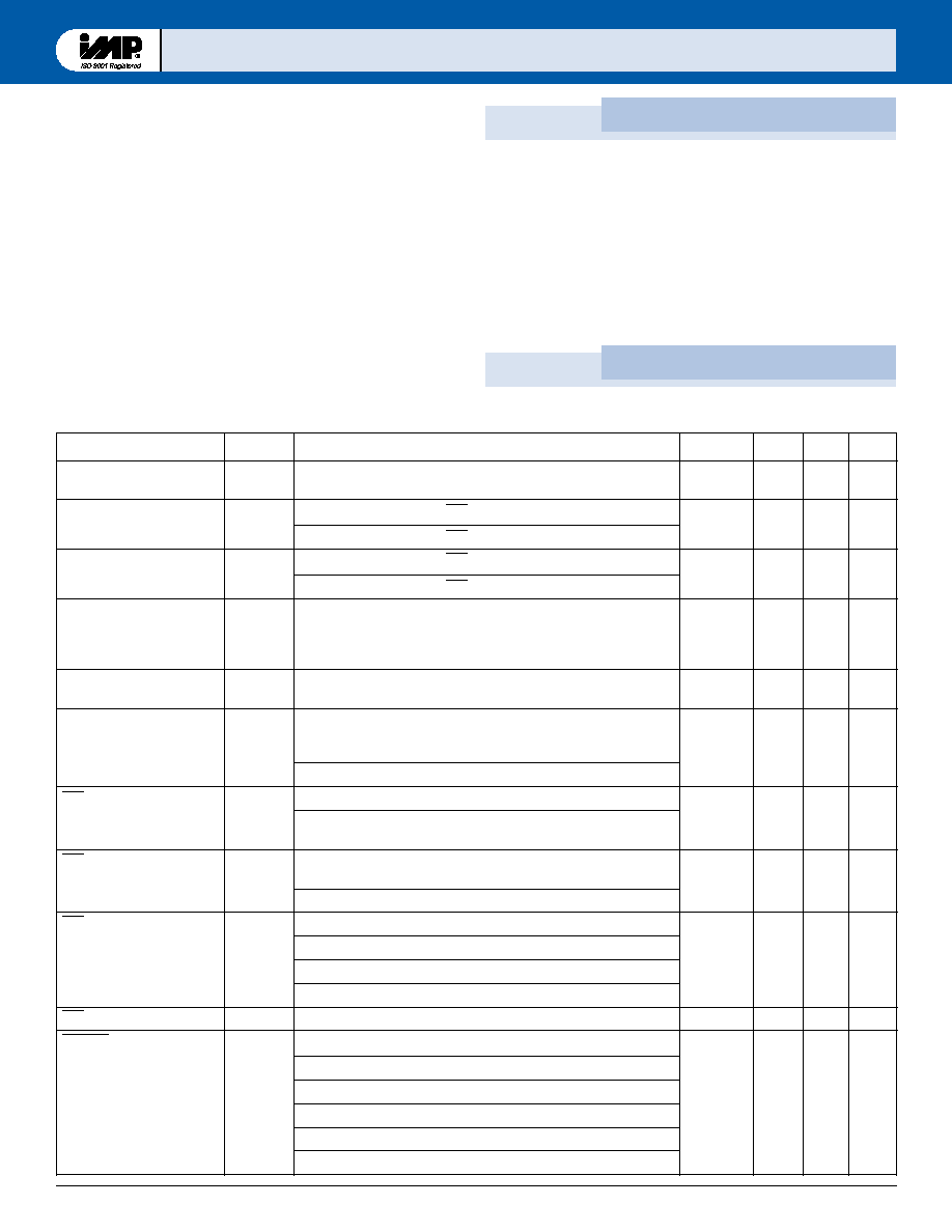
Pin Number
IMP706P
IMP706R/S/T/J IMP708R/S/T/J
DIP/SO MicroSO DIP/SO MicroSO DIP/SO MicroSO Name
Function
Manual reset input. The active LOW input triggers
a reset pulse. It is pulled HIGH by a 20k
pull-up
1
3
1
3
1
3
MR
resistor. It is compatible with TTL/CMOS signals
when V
CC
= 5V. It can be shorted to ground
through a mechanical switch. Leave floating or
connect to V
CC
if the function is not used.
2
4
2
4
2
4
V
CC
Monitored power supply input.
3
5
3
5
3
5
GND
Ground
Power-fail input voltage monitor. With PFI less than
4
6
4
6
4
6
PFI
1.25V, PFO goes LOW. Connect PFI to ground
when not used.
Power-fail output. The output is active LOW and
5
7
5
7
5
7
PFO
sinks current when PFI is less than 1.25V. If not
used, leave the pin unconnected.
Watchdog input. WDI controls the internal watchdog
timer. A HIGH or LOW signal for 1.6 sec at WDI
allows the internal timer to run-out, setting WDO low.
6
8
6
8
--
--
WDI
A rising or falling edge must occur at WDI within
1.6 seconds or WDO goes LOW. The watchdog
function is disabled by floating WDI. The internal
watchdog timer clears when: RESET is asserted;
WDI is three-stated; or WDI sees a rising or falling edge.
--
--
--
--
6
8
NC
Not connected.
Active-LOW reset output. Pulses LOW for 200ms
when triggered, and stays LOW whenever V
CC
is
--
--
7
1
7
1
RESET
below the reset threshold. RESET remains LOW for
200ms after V
CC
rises above the RESET threshold
or MR goes from HIGH to LOW. A watchdog timeout
will not trigger RESET unless WDO is connected to MR.
Watchdog output. WDO goes LOW when the 1.6
second internal watchdog timer times-out and does
not go HIGH until a transition occurs at WDI. In
8
2
8
2
--
--
WDO
addition, when V
CC
falls below the reset threshold,
WDO goes LOW. Unlike RESET, WDO does not have
a minimum pulse width and as soon as V
CC
exceeds
the reset threshold, WDO becomes HIGH with no delay.
7
1
--
--
8
2
RESET
Active-HIGH reset output. RESET is the inverse of
RESET.
IMP706P/R/S/T/J, IMP708R/S/T/J
IMP706P/R/S/T/J, IMP708R/S/T/J
Pin Descriptions
Feature Summary
©
1999 IMP, Inc.
408-432-9100/www.impweb.com
5
IMP706P IMP706R IMP706S IMP706T IMP706J IMP708R IMP708S IMP708T IMP708J
Power-fail detector
I
I
I
I
I
I
I
I
I
Brownout detection
I
I
I
I
I
I
I
I
I
Debounced manual RESET input
I
I
I
I
I
I
I
I
I
Power-up/down RESET
I
I
I
I
I
I
I
I
I
Watchdog timer
I
I
I
I
I
Active-HIGH RESET
I
Active-LOW RESET
I
I
I
I
Active-LOW and HIGH RESETs
I
I
I
I
RESET threshold
2.63V
2.63V
2.93V
3.08V
4.00V
2.63V
2.93V
3.08V
4.00V