
Key Features
Applications
3-Pin Microcontroller
Power Supply Supervisor
x
Embedded controllers
x
Battery operated systems
x
Intelligent instruments
x
Wireless communication systems
x
PDAs and handheld equipment
x
Improved Maxim MAX809/MAX810 replacement
-- Lower supply current...6µA
-- 80% lower maximum supply current
x
Monitor 5V, 3.3V and 3V supplies
x
140ms min. reset pulse width
x
Active-low reset valid with 1.1V supply
(IMP809)
x
Small 3-pin SOT-23 package
x
No external components
x
Specified over full temperature range
-- ≠40∞C to 105∞C
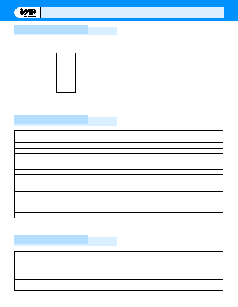
Block Diagrams
IMP809
(IMP810)
VCC
VCC
VCC
GND
GND
RESET
(RESET)
809/10_01.eps
µ
P
RESET
Input
The IMP809/IMP810 are 3.0V, 3.3V and 5.0V power supply supervisor cir-
cuits optimized for low-power microprocessor (µP), microcontroller (µC)
and digital systems. The IMP809/810 are improved drop-in replacements
for the Maxim MAX809/810 and feature 60% lower supply current.
A reset signal is issued if the power supply voltage drops below a preset
reset threshold and is asserted for at least 140ms after the supply has
risen above the reset threshold. The IMP809 has an active-low RESET
output that is guaranteed to be in the correct state for V
CC
down to 1.1V.
The IMP810 has an active-high RESET output. The reset comparator is
designed to ignore fast transients on V
CC
.
Low supply current makes the IMP809/IMP810 ideal for use in portable
and battery operated equipment. The IMP809/IMP810 are available in a
compact 3-pin SOT23 package.
Six voltage thresholds are available to support 3V to 5V systems:
IMP809, IMP8
IMP809, IMP8
1
1
0
0
P
OWER
M
ANAGEMENT
Reset Threshold
Suffix
Voltage (V)
L
4.63
M
4.38
J
4.00
T
3.08
S
2.93
R
2.63
IMP, Inc.
San Jose, CA
408-432-9100/www.impweb.com
2
IMP809, IMP8
IMP809, IMP8
1
1
0
0
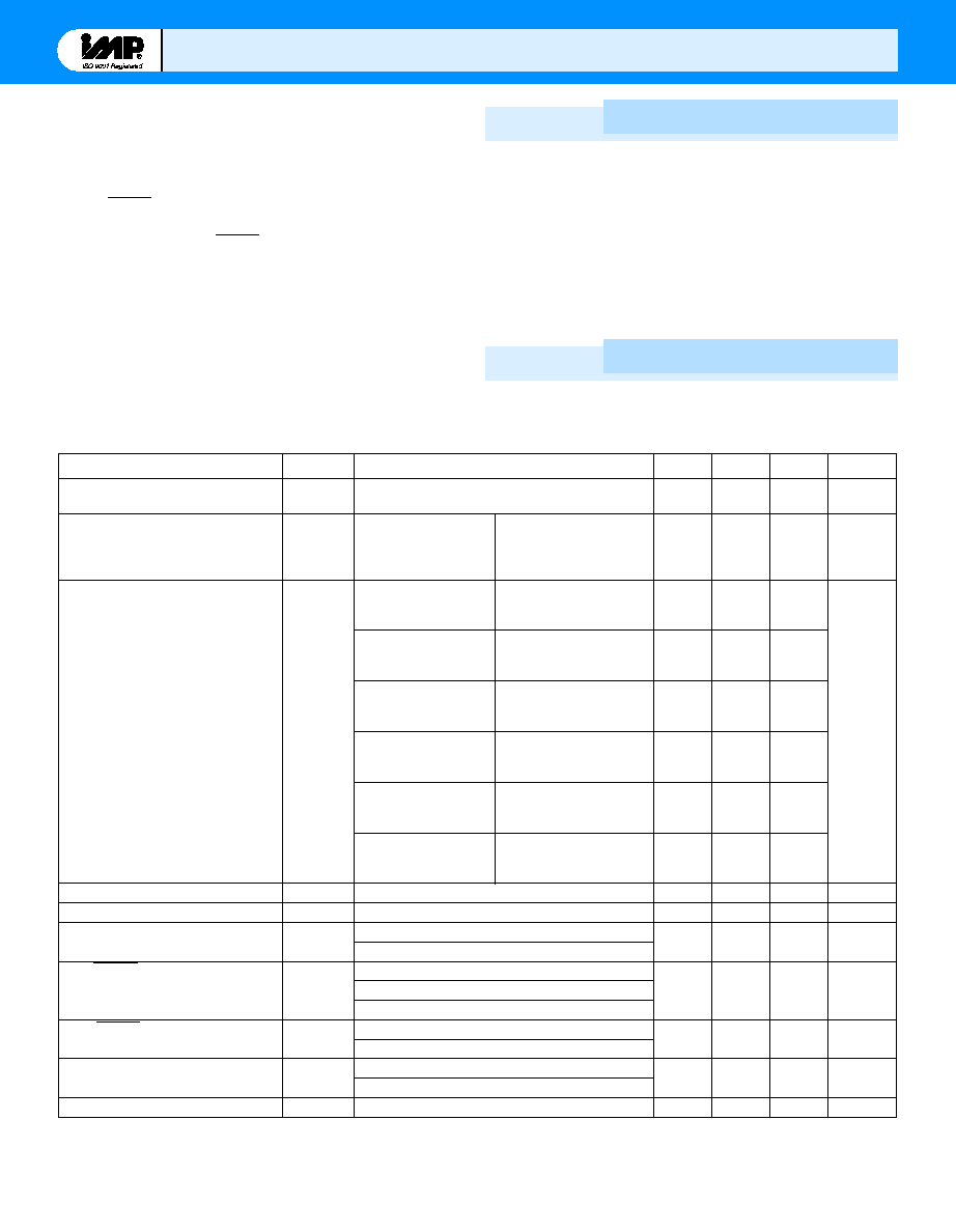
Ordering Information
Pin Configuration
IMP809
(IMP810)
GND
(RESET) RESET
V
CC
3
1
2
809/10_02.eps
SOT23
Package Marking
2
Part Number
1
Reset Threshold (V)
Temperature Range
Pin-Package
(XX Lot Code)
IMP809 Active LOW Reset
IMP809LEUR-T
4.63
≠ 40∞C to +105∞C
3-SOT23
AAXX
IMP809MEUR-T
4.38
≠ 40∞C to +105∞C
3-SOT23
ABXX
IMP809JEUR-T
4.00
≠ 40∞C to +105∞C
3-SOT23
CWXX
IMP809TEUR-T
3.08
≠ 40∞C to +105∞C
3-SOT23
ACXX
IMP809SEUR-T
2.93
≠ 40∞C to +105∞C
3-SOT23
ADXX
IMP809REUR-T
2.63
≠ 40∞C to +105∞C
3-SOT23
AFXX
IMP810 Active HIGH Reset
IMP810LEUR-T
4.63
≠ 40∞C to +105∞C
3-SOT23
AGXX
IMP810MEUR-T
4.38
≠ 40∞C to +105∞C
3-SOT23
AHXX
IMP810JEUR-T
4.00
≠ 40∞C to +105∞C
3-SOT23
AIXX
IMP810TEUR-T
3.08
≠ 40∞C to +105∞C
3-SOT23
AJXX
IMP810SEUR-T
2.93
≠ 40∞C to +105∞C
3-SOT23
AKXX
IMP810REUR-T
2.63
≠ 40∞C to +105∞C
3-SOT23
ALXX
2
Notes:
1. Tape and Reel packaging is indicated by the -T designation.
2. Devices may also be marked with full part number: 809L, 810M etc. XX refers to lot.
Related Products
IMP809
IMP810
IMP811
IMP812
Max. Supply Current
15µA
15µA
15µA
15µA
Package Pins
3
3
4
4
Manual RESET input
s
s
Package Type
SOT-23
SOT-23
SOT-143
SOT-143
Active-HIGH RESET output
s
s
Active-LOW RESET output
s
s
3
IMP809, IMP8
IMP809, IMP8
1
1
0
0
Parameter
Symbol Conditions
Min
Typ
Max
Units
Input Voltage (V
CC
) Range
V
CC
T
A
= 0∞C to 70∞C
1.1
5.5
V
T
A
= ≠ 40∞C to 105∞C
1.2
5.5
Supply Current
I
CC
T
A
= ≠ 40∞C to 85∞C
V
CC
< 5.5V, L/M/J
9
15
µA
T
A
= ≠ 40∞C to 85∞C
V
CC
< 3.6V, R/S/T
6
10
T
A
= 85∞C to 105∞C
V
CC
< 5.5V, L/M/J
25
T
A
= 85∞C to 105∞C
V
CC
< 3.6V, R/S/T
20
Reset Threshold
V
TH
L devices
T
A
= 25∞C
4.56
4.63
4.70
V
T
A
= ≠ 40∞C to 85∞C
4.50
4.75
T
A
= 85∞C to 105∞C
4.40
4.86
M devices
T
A
= 25∞C
4.31
4.38
4.45
T
A
= ≠ 40∞C to 85∞C
4.25
4.50
T
A
= 85∞C to 105∞C
4.16
4.56
J devices
T
A
= 25∞C
3.93
4.00
4.06
T
A
= ≠ 40∞C to 85∞C
3.89
4.10
T
A
= 85∞C to 105∞C
3.80
4.20
T devices
T
A
= 25∞C
3.04
3.08
3.11
T
A
= ≠ 40∞C to 85∞C
3.00
3.15
T
A
= 85∞C to 105∞C
2.92
3.23
S devices
T
A
= 25∞C
2.89
2.93
2.96
T
A
= ≠ 40∞C to 85∞C
2.85
3.00
T
A
= 85∞C to 105∞C
2.78
3.08
R devices
T
A
= 25∞C
2.59
2.63
2.66
T
A
= ≠ 40∞C to 85∞C
2.55
2.70
T
A
= 85∞C to 105∞C
2.50
2.76
Reset Threshold Stability
30
ppm/∞C
V
CC
to Reset Delay
V
CC
= V
TH
to V
TH
- 100mV
20
µs
Reset Active Timeout Period
V
OL
T
A
= ≠ 40∞C to 85∞C
140
240
560
ms
T
A
= 85∞C to 105∞C
100
840
Low RESET Output Voltage
(IMP809)
V
OL
V
CC
= V
TH
min., I
SINK
= 1.2mA, IMP809R/S/T
0.3
V
V
CC
= V
TH
min., I
SINK
= 3.2mA, IMP809L/M/J
0.4
V
CC
> 1.1V, I
SINK
= 50µA
0.3
High RESET Output Voltage
(IMP809)
V
OH
V
CC
> V
TH
max., I
SOURCE
= 500µA, IMP809R/S/T 0.8V
CC
V
V
CC
> V
TH
max., I
SOURCE
= 800µA, IMP809L/M/J V
CC
-1.5
Low RESET Output Voltage
(IMP810)
V
OL
V
CC
= V
TH
max., I
SINK
= 1.2mA, IMP810R/S/T
0.3
V
V
CC
= V
TH
max., I
SINK
= 3.2mA, IMP810L/M/J
0.4
High RESET Output Voltage
(IMP810)
V
OH
1.8V < V
CC
< V
TH
min., I
SOURCE
= 150µA
0.8V
CC
V
Absolute Maximum Ratings
Pin Terminal Voltage with Respect to Ground
V
CC
. . . . . . . . . . . . . . . . . . . . . . . . . . . . . . . . . ≠0.3V to 6.0V
RESET, RESET . . . . . . . . . . . . . . . . . . . . . . . . . ≠0.3V to (V
CC
+ 0.3V)
Input Current at V
CC
. . . . . . . . . . . . . . . . . . . 20mA
Output Current: RESET, RESET . . . . . . . . . 20mA
Rate of Rise at V
CC
. . . . . . . . . . . . . . . . . . . . 100V/µs
Power Dissipation (T
A
= 70
∞
C) . . . . . . . . . . 320mW
(Derate 4mW/∞C above 70
∞
C)
Operating Temperature Range . . . . . . . . . . ≠40∞C to 105∞C
Storage Temperature Range . . . . . . . . . . . . . ≠65∞C to 160∞C
Lead Temperature (soldering, 10 sec) . . . . . 300∞C
Electrical Characteristics
These are stress ratings only and functional operation is not implied.
Exposure to absolute maximum ratings for prolonged time periods may
affect device reliability
Unless otherwise noted V
CC
is over the full voltage range, T
A
= ≠40∞C to 105∞C.
Typical values at T
A
= 25∞C, V
CC
= 5V for L/M/J devices, V
CC
= 3.3V for T/S devices and V
CC
= 3V for R devices.
Notes:
1. Production testing done at T
A
= 25∞C. Over-temperature specifications guaranteed by design only.
2.
R
E
S
E
T output is active LOW for the IMP809 and RESET output is active HIGH for the IMP810

4
IMP809, IMP8
IMP809, IMP8
1
1
0
0
Pin Descriptions
Pin Number
Name
Function
1
GND
Ground
2
RESET
RESET is asserted LOW if V
CC
falls below the reset threshold and remains LOW for the
(IMP809)
240ms typical reset timeout period (140ms minimum) after V
CC
exceeds the threshold.
2
RESET
RESET is asserted HIGH if V
CC
falls below the reset threshold and remains HIGH for the
(IMP810)
240ms typical reset timeout period (140ms minimum) after V
CC
exceeds the threshold.
3
V
CC
Power supply input voltage (3.0V, 3.3V, 5.0V)
5V
0V
5V
0V
V
CC
V
TH
RESET
140ms
minimum
Active Reset
Timeout Period
5V
0V
RESET
IMP809
IMP810
809/10_03.eps
Reset Timing
The reset signal is asserted≠LOW for the IMP809 and HIGH for the
IMP810≠when the V
CC
signal falls below the threshold trip voltage
and remains asserted for 140ms minimum after the V
CC
has risen
above the threshold.
Detailed Descriptions
Figure 1. Reset Timing Diagram

5
IMP809, IMP8
IMP809, IMP8
1
1
0
0
Bi-directional Reset Pin Interfacing
The IMP809/810 can interface with µP/µC bi-directional reset
pins by connecting a 4.7k
resistor in series with the
IMP809/810 reset output and the µP/µC bi-directional reset pin.
Negative V
CC
Transients
The IMP809/810 protect µPs from brownouts and low V
CC
. Short
duration transients of 100mV amplitude and 20µs or less duration
typically do not cause a false RESET.
To ensure logic inputs connected to the IMP809 RESET pin are in
a known state when V
CC
is under 1.1V, a 100k
pull-down
resistor at RESET is needed. The value is not critical. A pull-up
resistor to V
CC
is needed with the IMP810.
Power
Supply
IMP810
VCC
GND
RESET
100k
809/10_05.eps
Valid Reset with V
CC
under 1.1V
Power
Supply
IMP809
VCC
GND
RESET
100k
809/10_04.eps
Power
Supply
IMP809
VCC
GND
GND
RESET
4.7k
809/10_06.eps
Bi-directional I/O Pin
(Example: 68HC11)
BUF
Buffered
RESET
µ
C or
µ
P
RESET
Input
Application Information
Figure 2. RESET Valid with V
CC
Under 1.1V
Figure 3. RESET Valid with V
CC
Under 1.1V
Figure 4. Bi-directional Reset Pin Interfacing