 | –≠–ª–µ–∫—Ç—Ä–æ–Ω–Ω—ã–π –∫–æ–º–ø–æ–Ω–µ–Ω—Ç: ILC1832M | –°–∫–∞—á–∞—Ç—å:  PDF PDF  ZIP ZIP |

ILC1832
µP Supervisory Circuit
Impala Linear Corporation
Impala Linear Corporation
1
(408) 574-3939
www.impalalinear.com
October 1999
ILC1832 1.1
The ILC1832 is a multifunction circuit which monitors micro-
processor activity, external reset and power supplies in
microprocessor based systems. Ths circuit functions
include a watchdog timer, power supply monitor, micro-
processor reset, and manual pushbutton reset input.
The power supply line is monitored with a comparator and
an internal voltage reference. RST is forced low when an
out-of-tolerance condition exists and remains asserted for
at least 250ms after V
CC
rises above the threshold voltage
(2.55V or 2.88V). The RST pin will remain logic low with
V
CC
as low as 1.4V.
The Watchdog input (ST) monitors µP activity and will assert
RST if no µP activity has occurred within the watchdog time-
out period. The watchdog timeout period is selectable with
nominal periods of 150, 600, or 1200 milliseconds.
∑ Power OK/Reset Time Delay, 250ms min.
∑ Watchdog Timer, 150 ms, 600ms, or 1.2s Typical
∑ Precision Supply Voltage Monitor, Select Between 5%
or 10% of Supply Voltage
∑ 18µA Supply Current
∑ Debounced External Reset Input
∑ 8-Pin SOIC or DIP Package
∑ Computers
∑ Controllers
∑ Critical Microprocessor Power Monitoring
∑ Intelligent Instruments
∑ Portable Equipment
ILC1832
V
CC
Top View
PBRST
RST
TD
2
1
8
6
RST
GND
ST
TOL
4
3
5
7
ETC1832N - 8 Lead Plastic DIP Package
ETC1832M - 8 Lead Plastic SOIC Package
ILC1832
µ
µ
P
V
CC
V
CC
V
CC
ST
RESET
PBRST
RST
TD
GND
TOL
I/O
Part
Package
Temp. Range
ILC1832N
8-Lead PDIP
-40∞C to +85∞C
ILC1832M
8-Lead SOIC
-40∞C to +85∞C
General Description
Features
Applications
Ordering Information
Typical Circuit
Pin-Package Configurations
Preliminary

Parameter
Symbol
Ratings
Units
V
CC
-0.3 to 7.0
V
Terminal Voltage
All other inputs
-0.3 to (V
CC
+ 0.3)
V
V
CC
250
mA
Input Current
GND All other inputs
25
mA
Operating Temperature Range
T
A
-40 to +85
∞C
Storage Temperature Range
-65 to +150
∞C
Lead Temperature (Soldering, 10 sec.)
300
∞C
Power Dissipation
700
mW
Parameter
Conditions
Min
Typ
Max
Units
Supply Voltage Range, V
CC
5.5
V
Supply Current, I
CC
V
CC
= 5V (See Note 1)
V
CC
= 3.3V (See Note 1)
18
15
30
25
µ
A
ST and PBRST Input Levels
V
IH
, V
CC
> 2.7V
V
IH
, V
CC
< 2.7V
V
IL
2.0
V
CC
≠0.4
-0.3
V
CC
+ 0.3
V
CC
+ 0.3
0.5
V
Input Leakage PBRST, I
IL
(See Note 2)
±1
µ
A
Output Voltage, RST, RST
I
SOURCE
= 350µA, V
CC
= 3.3V
2.4
V
Output Voltage, RST, RST
I
SINK
= 10mA, V
CC
= 3.3V
0.4
V
Output Voltage, RST
I
SINK
= 50µA, V
CC
= 1.4V
0.3
V
V
CC
5% Trip Point (Reset Threshold Voltage)
TOL= GND
2.80
2.88
2.97
V
V
CC
10% Trip Point (Reset Threshold Voltage)
TOL= V
CC
2.47
2.55
2.64
V
Input Capacitance, ST, TOL
C
IN
(See Note 3)
5
pF
Output Capacitance, RST, RST
C
OUT
(See Note 3)
7
pF
PBRST Min. Pulse Width, t
PB
PBRST = V
IL
(See note 4)
20
ms
PBRST Delay, t
PBD
1
4
20
ms
Reset Active Time, t
RST
250
610
1000
ms
ST Pulse Width, t
ST
20
ns
ST Timeout Period, t
TD
TD = 0V
TD = Open
TD = V
CC
62.5
250
500
150
600
120
0
250
1000
2000
ms
V
CC
Fall Time, t
F
40
µ
s
V
CC
Rise Time, t
R
0
ns
V
CC
Detect to RST Low and RST High, tRPD
V
CC
Falling at 1.66 mV/
µ
s
5
8
µ
s
V
CC
Detect to RST Open and RST Low, tRPU
V
CC
Rising
250
610
1000
ms
V
CC
= 3 to 5.5V, T
A
= Operating Temperature Range, unless otherwise noted.
Stresses above those listed under ABSOLUTE MAXIMUM RATINGS may cause permanent device failure. Functionality at
or above these limits is not implied. Exposure to absolute maximum ratings for extended periods may affect device reliability.
Operating ranges define those limits between which the functionality of the device is guaranteed.
Note 1: I
CC
is measured with PBRST and all outputs open and inputs within 0.5V of supply rails.
Note 2: PBRST has an internal 40k
(typical) pull-up resistor to V
CC
.
Note 3: Guaranteed by design at T
A
= 25∞C.
Note 4: PBRST must be held low for a minimum of 20ms to guarantee a reset.
µP Supervisory Circuit
Preliminary
Impala Linear Corporation
2
(408) 574-3939
www.impalalinear.com
October 1999
ILC1832 1.1
Electrical Characteristics
Absolute Maximum Ratings

Pin
Number
Pin
Name
Description
1
PBRST
Pushbutton reset input. This input is debounced and can be driven with external logic
signals or a mechanical pushbutton to actively force a reset. All pulses less than 1ms in
duration on the PBRST pin are ignored. Any pulse with a duration of 20ms or greater is
guaranteed to cause a reset. PBRST has an internal 40k
(typical) pull-up resistor to V
CC
.
2
TD
Time delay input. This input selects the timebase used by the watchdog timer. When TD =
0V, the watchdog timeout period is set to a nominal value of 150ms, when TD = open, the
watchdog timeout period is set to a nominal value of 600ms and when TD = V
CC
, the
watchdog timeout period is 1.2 sec nominally.
3
TOL
Tolerance select input. Selects whether 5% or 10% of V
CC
is used as the reset threshold
voltage. When TOL = 0V, the 5% tolerance level is selected and when TOL = V
CC
, a 10%
tolerance level is selected.
4
GND
Ground pin, 0V reference.
5
RST
RST is asserted high if either V
CC
goes below the reset threshold, the watchdog times out or
PBRST is pulled low for a minimum of 20ms. RST remains asserted for one reset timeout
period after V
CC
exceeds the reset threshold or after the watchdog times out or after PBRST
goes high.
6
RST
RST is asserted low if either V
CC
goes below the reset threshold, the watchdog times out or
PBRST is pulled low for a minimum of 20ms. RST remains asserted for one reset timeout
period after V
CC
exceeds the reset threshold or after the watchdog times out or after PBRST
goes high. Open-drain output.
7
ST
Input to the watchdog timer. If ST does not see a transition from high to low within the
watchdog timeout period, RST and RST will be asserted.
8
V
CC
Power supply input.
8
1
Reset
Generator
6
4
-
+
V
CC
ST
RST
GND
3
7
2
Trip Point
Select
Ref
Manual Reset
Debounce
Watchdog
Timer
Timeout
Select
5
RST
TOL
PBRST
TD
µP Supervisory Circuit
Preliminary
Pin Functions
Block Diagram
Impala Linear Corporation
3
(408) 574-3939
www.impalalinear.com
October 1999
ILC1832 1.1

Pushbutton Reset Input
The PBRST input can be driven with a manual pushbutton
switch or with external logic signals. The input is internally
debounced and requires an active low signal to force the
reset outputs into their active states. The PBRST input will
recognize any pulse that is 20ms in duration or greater and
will ignore all pulses that are less than 1ms in duration.
Power Monitor
The RST and RST pins are asserted whenever V
CC
falls
below the reset threshold voltage set by the TOL pin. A 5%
tolerance level (2.88V reset threshold voltage) can be
selected by connecting the TOL pin to ground or a 10% tol-
erance (2.55V reset threshold voltage) can be selected by
connecting the TOL pin to V
CC
. The reset pins will remain
asserted for a period of 250ms after V
CC
has resen above
the reset threshold voltage. The reset function ensures the
microprocessor is properly reset and powers up into a
known condition after a power failure. RST will remain valid
with V
CC
as low as 1.4V.
Watchdog Timer
The microprocessor can be monitored by connecting the ST
pin (watchdog input) to a bus line or I/O line. If a high-to-
low transition does not occur on the ST pin within the watch-
dog timeout period set by the TD pin (see Table 1), the RST
and RST pins will be asserted rsulting in a microprocessor
reset. RST and RST will remain asserted for 250ms when
this occurs. A minimum pulse of 75ns or any transition
high-to-low on the ST pin will reset the watchdog timer. The
watchdog timer will be reset if ST sees a valid transition
within the watchdog timeout period.
RST
t
RPD
V
CCTP
V
CCTP
t
RPU
V
CC
RST
RST
t
PDLY
t
RST
PBRST
RST
t
PB
t
TD
TD Pin
Min.
Typ.
Max.
GND
62.5 ms
150 ms
250 ms
Open
250 ms
600 ms
1000 ms
V
CC
500 ms
1200 ms
2000 ms
Industry P/N
ILC Direct Replacement
DS1832
ILC1832N
DS1832S
ILC1832M
t
SD
ST
t
TD
Power-Up/Power-Down Sequence
Watchdog Input
Pushbutton Reset
µP Supervisory Circuit
Preliminary
Circuit Description
Alternate Source Reference Guide
Impala Linear Corporation
4
(408) 574-3939
www.impalalinear.com
October 1999
ILC1832 1.1
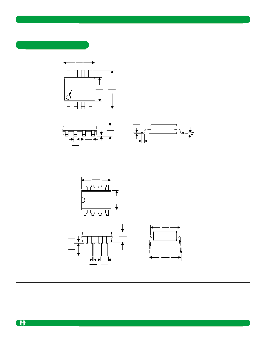
Pin 1 identifier
0.197
0.190
0.155
0.150
0.244
0.228
0.069
0.053
0.011
0.004
0.060
0.040
0.019
0.013
0.050
0.016
0.012
0.009
0.8∞
M Package, 8-Pin Small-Outline
0.260
0.240
0.019
0.013
0.260
0.240
0.260
0.240
0.260
0.240
0.260
0.240
0.260
0.240
0.260
0.240
0.260
0.240
N Package, 8-Pin Plastic Dual In-Line
Devices sold by Impala Linear Corporation are covered by the warranty and patent indemnification provisions appearing
in its Terms of Sale only. Impala Linear Corporation makes no warranty, express, statutory, implied, or by description
regarding the information set forth herein or regarding the freedom of the described devices from patent infringement.
Impala Linear Corporation makes no warranty of merchantability or fitness for any purpose. Impala Linear Corporation
reserves the right to discontinue production and change specifications and prices at any time and without notice.
This product is intended for use in normal commercial applications. Applications requiring an extended temperature
range, unusual environmental requirements, or high reliability applications, such as military and aerospace, are specif-
ically not recommended without additional processing by Impala Linear Corporation.
Impala Linear Corporation assumes no responsibility for the use of any circuitry other than circuitry embodied in an
Impala Linear Corporation product. No other circuits, patents, licenses are implied.
Life Support Policy
Impala Linear Corporation's products are not authorized for use as critical components in life support devices or systems.
1. Life support devices or systems are devices or systems which, (a) are intended for surgical implant into the body, or
(b) support or sustain life, and whose failure to perform, when properly used in accordance with instructions for use pro-
vided in the labelling, can be reasonably expected to result in a significant injury to the user.
2. A critical component is any component of a life support device or system whose failure to perform can be reason-
bly expected to cause the failure of the life support device or system, or to affect its safety or effectiveness.
µP Supervisory Circuit
Preliminary
Packaging Information
Impala Linear Corporation
5
(408) 574-3939
www.impalalinear.com
October 1999
ILC1832 1.1