
V
OUT
V
DD
V
REF
4~5mV
+
+
-
-
2-STEP PFM
CONTROLLED OSC
100/155kHz
V
LX
LIMITER
BUFFER
V
SS
L
X
EXT
CE
CHIP ENABLE
50 mA boost converter using Pulse Frequency Modulation,
or PFM, technique, in 5-lead SOT-89 or a 5-lead SOT-23
package. Only 3 external components are needed to com-
plete the switcher design.
The ILC6390 automatically senses load variations to choose
between 55% and 75% duty cycles. Normal operation is 55%
duty at 155kHz; when load currents exceed the internal com-
parator trip point, a "turbo mode" kicks in to provide extend-
ed on-time switching (75% duty at 100kHz oscillation).
Requiring only 30�A of supply current, the ILC6390
achieves efficiencies as high as 85% at 5V yet shuts down
to 0.5�A max.
Standard voltages offered are 2.5, 3.3, and 5.0V and is
available in both a 5 lead SOT-23 and 5 lead SOT-89 pack-
age for small footprint applications.
In addition, the ILC6391 is configured to drive an external
transistor to achieve higher power levels.
ILC6390/91
SOT-89 Step-Up PFM Switcher
with Auto-Load Sense
Impala Linear Corporation
Impala Linear Corporation
1
(408) 574-3939
www.impalalinear.com
Feb 2001
ILC6390 1.1
� 85% conversion efficiency at 50mA out
� Start-up voltages as low as 900mV
� �2.5% accurate outputs
� Complete switch design with only 3 external components
� Automatically senses load variations to select the optimal
duty cycle and extend conversion efficiencyover a wide
range
� External transistor configuration to run as switcher
controller
� Shutdown to 0.5�A
� Cellular phones, pagers
� Cameras, video recorders
� Palmtops and PDAs
ILC6390CM
ILC6390CP
5
4
1
2
3
SOT-25
(TOP VIEW)
L
X
V
SS
CE
V
DD
N/C
V
SS
L
X
SOT-89-5
(TOP VIEW)
5
4
1
2
3
N/C
V
OUT
CE
ILC6391CM
5
4
1
2
3
SOT-25
(TOP VIEW)
L
X
V
SS
CE
V
DD
N/C
ILC6391CP
V
SS
L
X
SOT-89-5
(TOP VIEW)
5
4
1
2
3
N/C
V
OUT
CE
Block Diagram
Pin-Package Configurations
ILC6390CM-25
2.5V � 2.5%
ILC6390CM-33
3.3V � 2.5%
ILC6390CM-50
5.0V � 2.5%
ILC6391CM-25
3.3V � 2.5% driving external transistor
ILC6391CM-33
3.3V � 2.5% driving external transistor
ILC6391CM-50
5.0V � 2.5% driving external transistor
ILC6390CP-25
2.5V � 2.5%
ILC6390CP-33
3.3V � 2.5%
ILC6390CP-50
5.0V � 2.5%
ILC6391CP-25
3.3V � 2.5% driving external transistor
ILC6391CP-33
3.3V � 2.5% driving external transistor
ILC6391CP-50
5.0V � 2.5% driving external transistor
* Standard product offering comes in tape & reel, quantity 3000 per
reel, orientation right for SOT-25, quantity 1000 per reel orientation
right for SOT-89.
General Description
Features
Applications
Ordering Information

SOT-89 Step-Up PFM Switcher with Auto-Load Sense
Impala Linear Corporation
2
(408) 574-3939
www.impalalinear.com
Feb 2001
ILC6390 1.1
Parameter
Symbol
Ratings
Units
V
OUT
Input Voltage
V
OUT
12
V
Voltage on pin L
X
VL
X
12
V
Current on pin L
X
IL
X
400
mA
Voltage on pin EXT
V
EXT
V
SS
-0.3~V
OUT
+0.3
V
Current on pin EXT
I
EXT
�50
mA
CE Input Voltage
V
CE
12
V
V
DD
Input Voltage
V
DD
12
V
Continuous Total Power Dissipation
P
D
(SOT-25)
P
D
(SOT-89)
150
500
mW
Operating Ambient Temperature
T
opr
-30~+80
�C
Storage Temperature
T
stg
-40~+125
�C
Parameter
Symbol
Conditions
Min
Typ
Max
Units
Output Voltage
V
OUT
Test Circuit of Figure 1
4.875
5.000
5.125
V
Input Voltage
V
IN
10
V
Oscillation Startup Voltage
V
ST
I
OUT
= 1mA
0.80
0.9
V
Oscillation Hold Voltage
V
HLD
I
OUT
= 1mA
0.70
V
NO-Load Input Current
I
IN
I
OUT
= 0mA
(See Note 1)
5.3
10.6
�A
Supply Current 1 (See Note 2)
I
DD
1
V
OUT
= 4.75V
31.7
63.4
�A
Supply Current 2
I
DD
2
V
OUT
= 5.5V
2.4
4.8
�A
L
X
Switch-On Resistance
R
SWON
V
OUT
= 4.75V, VL
X
= 0.4
2.8
4.3
L
X
Leakage Current
I
LXL
No external components, V
OUT
=
VL
X
= 10V
1.0
�A
Duty Ratio 1
DUTY 1
V
OUT
= 4.75V, Measuring of L
X
waveform
70
75
80
%
Duty Ratio 2
DUTY 2
V
OUT
= 4.75V, Measuring of L
X
on-time
50
55
60
%
Maximum Oscillation Freq. 1
MFO 1
V
OUT
= 4.75V, 75% duty
85
100
115
kHz
Maximum Oscillation Freq. 2
MFO 2
V
OUT
= 4.75V, 55% duty
153
180
207
kHz
Stand = by Current
I
STB
V
OUT
= 4.75V
0.5
�A
CE "High" Voltage
V
CEH
V
OUT
= 4.75V, Existance of L
X
Oscillation
0.75
V
CE "Low" Voltage
V
CEL
V
OUT
= 4.75V, Disappearance of
L
X
Oscillation
0.20
V
CE "High" Current
I
CEH
V
CE
= V
OUT
x 0.95
0.25
�A
CE "Low" Current
I
CEL
V
OUT
= 4.75V, V
CE
= 0V
-0.25
�A
L
X
Limit Voltage
V
LXLMT
V
OUT
= 4.75V, fosc > MFO x 2
(See Note 3)
0.7
1.1
V
Note:
1. The Schottky diode (S.D.), in figure 3 must be type MA735, with Reverse current (IR) < 1.0�A at reverse voltage (VR)=10.0V
2. "Supply Current 1" is the supply current while the oscillator is continuously oscillating. In actual operation the oscillator periodically operates which
results in less average power consumption.
The current that is actually provided by external V
IN
source is represented by "No-Load Input Current"
3. The switching frequency is determined by the delay time of the internal comparator and MFO1, which sets the min. on-time
Absolute Maximum Ratings (T
A
= 25�C)
Electrical Characteristics ILC6390
V
OUT
= 5.0V T
A
= 25�C. Unless otherwise specified, V
IN
= V
OUT
x 0.6, I
OUT
= 50mA. See schematic, fig. 3.

SOT-89 Step-Up PFM Switcher with Auto-Load Sense
Impala Linear Corporation
3
(408) 574-3939
www.impalalinear.com
Feb 2001
ILC6390 1.1
Parameter
Symbol
Conditions
Min
Typ
Max
Units
Output Voltage
V
OUT
Test Circuit of Figure 4
4.875
5.000 5.125
V
Input Voltage
V
IN
10
V
Operation Startup Voltage
V
ST
I
OUT
= 1mA
0.80
0.9
V
Operation Hold Voltage
V
ST
I
OUT
= 1mA
0.70
V
Supply Current 1
(See Note 1)
I
DD
1
V
OUT
= 4.75V
31.7
63.4
�A
Supply Current 2
I
DD
2
V
OUT
= 5.5V
2.4
4.8
�A
EXT "High" On-Resistance
R
EXTH
V
OUT
= 4.75V, V
EXT
= V
OUT
-0.4
50
75
EXT "Low" On-Resistance
R
EXTL
V
OUT
= 4.75V, V
EXT
= 0.4
50
75
Duty Ratio 1
DUTY 1
V
OUT
= 4.75V, Measuring of
EXT waveform
70
75
80
%
Duty Ratio 2
DUTY 2
V
IN
= V
OUT
x 0.95, I
OUT
= 1mA,
Measuring of EXT High State
50
55
60
%
Maximum Oscillation Freq. 1
MFO 1
V
OUT
= 4.75V, 75% duty
85
100
115
kHz
Maximum Oscillation Freq. 2
MFO 2
V
IN
= V
OUT
x 0.95, 55% duty
153
180
207
kHz
Stand = by Current
I
STB
V
OUT
= 4.75V
0.5
�A
CE "High" Voltage
V
CEH
V
OUT
= 4.75V, Existence of
EXT Oscillation
0.75
V
CE "Low" Voltage
V
CEL
V
OUT
= 4.75V, Disappearance
of EXT Oscillation
0.20
V
CE "High" Current
I
CEH
V
CE
= V
OUT
= 4.75V
0.25
�A
CE "Low" Current
I
CEL
V
OUT
= 4.75V, V
CE
= 0V
-0.25
�A
Efficiency
EFFI
Test Circuit Figure 4
85
%
Note:
1. "Supply Current 1" is the supply current while the oscillator is continuously oscillating. In actual operation the oscillator periodically operates
which results in less average power consumption.
Electrical Characteristics ILC6391
V
OUT
= 5.0V T
A
= 25�C. Unless otherwise specified, V
IN
= V
OUT
x 0.6, I
OUT
= 50mA. See schematic, Fig.4
SOT-89 Step-Up PFM Switcher with Auto-Load Sense
Impala Linear Corporation
4
(408) 574-3939
www.impalalinear.com
Feb 2001
ILC6390 1.1
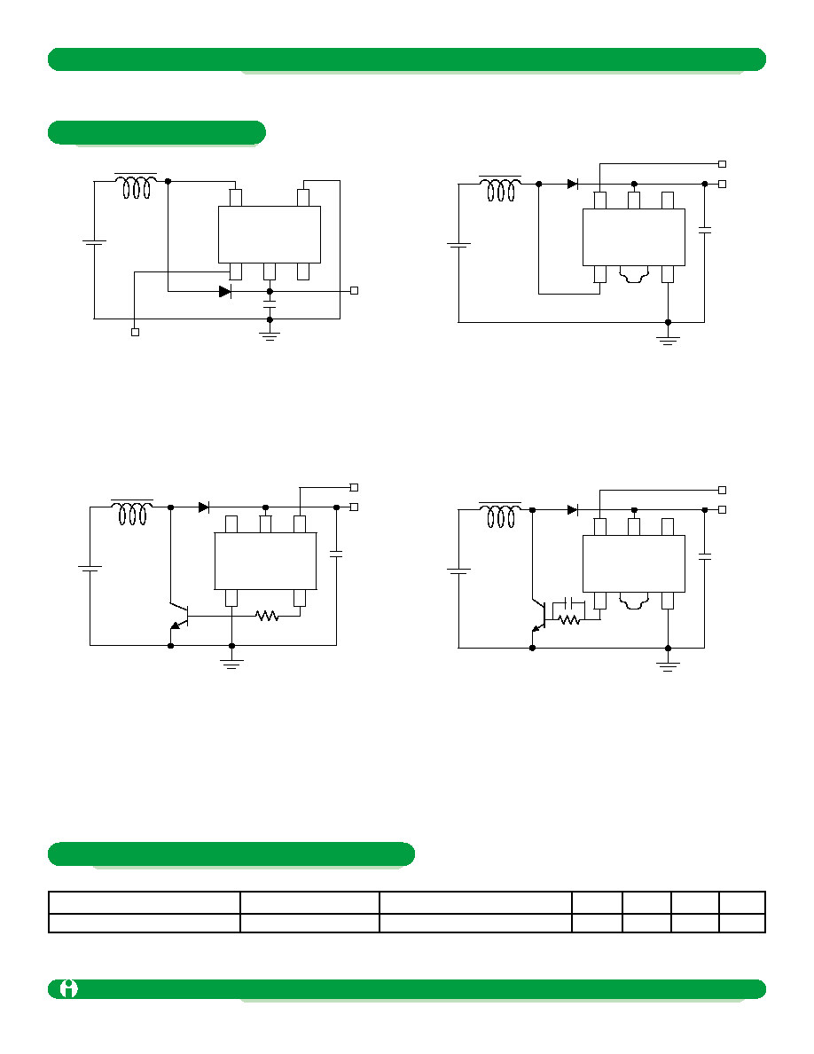
2
ILC6390CM
1
3
1
3
L
V
IN
GND
CE
SD
+
C
L
V
OUT
ILC6391CP
1
2
3
4
5
CE
V
OUT
C
L
+
L
SD
V
IN
GND
C
B
R
B
Tr
ILC6391CM
1
2
3
4
5
CE
V
OUT
C
L
+
L
SD
V
IN
GND
R
Tr
ILC6390CP
1
2
3
4
5
CE
V
OUT
C
L
+
L
SD
V
IN
GND
L: 100�H (SUMIDA, CD-54
SD: Diode (Schottky diode; MATSUSHITA MA 735)
C
L
: 16V 47�F (Tantalum Capacitor; NICHICON, f93)
L: 47�H (SUMIDA, CD-54)
SD: Diode (Schottky diode; MATSUSHITA MA735)
C
L
: 16V 47�F (Tantalum Capacitor; NICHICON, F93)
R
B
: 1k
C
B
: 3300pF
Tr: 2SC3279, 2SDI628G
Parameter
Efficiency
Symbol
EFFI
Conditions
Test Circuit of Figure 3
Units
%
Max
Typ
85
Min
Application Circuits
Electrical Characteristics ILC6390
V
OUT
= 5.0V T
A
= 25�C. Unless otherwise specified, V
IN
= V
OUT
x 0.6, I
OUT
= 50mA. See schematic, fig. 3.

SOT-89 Step-Up PFM Switcher with Auto-Load Sense
Impala Linear Corporation
5
(408) 574-3939
www.impalalinear.com
Feb 2001
ILC6390 1.1
The ILC6390 performs boost DC-DC conversion by controlling the
switch element shown in the circuit below.
When the switch is closed, current is built up through the inductor.
When the switch opens, this current has to go somewhere and is
forced through the diode to the output. As this on and off switch-
ing continues, the output capacitor voltage builds up due to the
charge it is storing from the inductor current. In this way, the out-
put voltage gets boosted relative to the input. The ILC6390 mon-
itors the voltage on the output capacitor to determine how much
and how often to drive the switch.
In general, the switching characteristic is determined by the output
voltage desired and the current required by the load. Specifically
the energy transfer is determined by the power stored in the coil
during each switching cycle.
P
L
= (t
ON
, V
IN
)
The ILC6390 and ILC6391 use a PFM or Pulse Frequency
Modulation technique. In this technique, the switch is always
turned on for a fixed period of time, corresponding to a fixed
switching frequency at a predefined duty cycle. For the ILC6390
this value is 3.55msec on time, corresponding to 55% duty cycle
at 155kHz. Because the inductor value, capacitor size, and
switch on-time and frequency are all fixed, the ILC6390 in essence
delivers the same amount of power to the output during each
switching cycle. This in turn creates a constant output voltage
ramp which is dependent on the output load requirement. In this
mode, the only difference between the PFM and PWM techniques
is the duty cycle of the switch.
Once the output voltage reaches the set point, the ILC6390 will
shut off the switch oscillator and wait until the output voltage
drops low again, at which point it will re-start the oscillator. As
you can see in the diagram, the PFM boost converter actually
skips pulses as a way of varying the amount of power being deliv-
ered to the output.
Because of this, PFM is sometimes called "Pulse Skipping
Modulation."
The chief advantage of using a PFM technique is that, at low cur-
rents, the switcher is able to maintain regulation without con-
stantly driving a switch on and off. This power savings can be
5mA or more for the ILC6390 versus the ILC6370, and at very
light loads this current difference can make a noticeable impact
on overall efficiency.
However, because the ILC6390 will skip pulses based on
load current, the effective frequency of switching may well
drop into the audio band. This means that the radiated
noise of the ILC6390 may interfere with the audio channel
of the system and additional filtering may be necessary. In
addition, because the PFM on-time is fixed, it usually has
higher output ripple voltage than the PWM switcher, which
dynamically changes the on-time to match the load current
requirements. [Ripple is due to the output cap constantly
accepting and storing the charge received from the induc-
tor, and delivering charge as required by the load. The
"pumping" action of the switch produces a sawtooth-
shaped voltage as seen by the output.]
On the plus side, because pulses are skipped, overtone content of
the frequency noise is lower than in a PWM configuration. The
sum of these characteristics for PFM converters makes it the ideal
choice for low-current or ultra-long runtime applications, where
overall conversion efficiency at low currents is of primary concern.
[For other conversion techniques, please see the ILC6370/71 and
ILC6380/81 datasheets.]
Dual-Step Mode
The ILC6390 and ILC6391 have one other unique feature, that
being to automatically switch to a second switching scheme in the
presence of heavy output loading. As we mentioned, the stan-
dard switching scheme for these parts is a 3.55msec, 155kHz,
55% duty cycle part. However, if the device detects that the out-
put load increases beyond a set point (as seen by the voltage
drop on the output capacitor), it switches in a 7.5msec, 100kHz,
75% duty cycle "turbo mode" specifically to keep up with the
increased load demand. This switchover is seamless to the user,
but will result in a change in the output ripple voltage characteris-
tic of the DC-DC converter.
PFM converters are widely used in portable consumer applica-
tions not requiring a high current level and relatively unaffected by
audio noise. Applications such as pagers and PDAs, which need
to operate in stand-by for extended periods of time, gravitate
toward the advantages of PFM since maximum run-time is a chief
differentiating element. The ILC6390 addresses this low-current
requirement, and additionally offers a "turbo" mode which main-
tains output regulation in the presence of heavier-than-normal
load currents, and maintains 0.5mA shutdown currents.
The only difference between the ILC6390 and ILC6391 parts is
that the 6391 is configured to drive an external transistor as the
switch element. Since larger transistors can be selected for this
element, higher effective loads can be regulated.
V
SET
V
OUT
Switch Waveform