
Dual 125mA CMOS LDO in an SO-8 package. This part
offers 120mV dropout voltage on each output at 100mA typ-
ical (5V part), and nearly zero dropout below 5mA. Each
output is independently short-circuit protected.
Its all-CMOS design means that only 2.2µA of current is
required to run the part.
±2% accurate outputs come in a number of configurations,
to allow for flexible yet compact portable system designs.
ILC7262
Dual CMOS LDO
Impala Linear Corporation
Impala Linear Corporation
1
(408) 574-3939
www.impalalinear.com
June 1996
ILC7262 1.0
∑ All-CMOS design in an 8-lead SOIC package
∑ ±2% precision outputs
∑ 2.2µA of Iq
∑ Short-circuit protected outputs
∑ Voltage options allow:
Dual 50mA 5.0 & 3.3V Regulator
Dual 50mA 5.0 & 3.0V Regulator
Dual 125mA 5V to 3.0V & 3.3V Convertor
∑ Battery-powered Equipment
∑ Portable communications
∑ PDAs and palmtops
ILC7262CS-50/30
Dual 50mA 5v & 3.0V Regulator
ILC7262CS-50/33
Dual 50mA 5V & 3.3V Regulator
ILC7262CS-33/30
Dual 125mA 5V to 3.0 V & 3.3V Converter
*Standard Product offering comes in tape & reel, quantity 1000 per reel, orientation right.
REFERENCE VOLTAGE
SOURCE
V
OUT
1
V
IN
-
+
SHORT-CIRCUIT
PROTECT
V
SS
V
OUT
2
V
SS
2
NC
V
SS
1
V
SS
2
NC
V
IN
V
OUT
1
V
OUT
2
NC
1
2
3
4
5
6
7
8
SO-8
(TOP VIEW)
Block Diagram
General Description
Features
Applications
Ordering Information
Pin-Package Configurations

Dual CMOS LDO
Impala Linear Corporation
2
(408) 574-3939
www.impalalinear.com
June 1996
ILC7262 1.0
Parameter
Symbol
Ratings
Units
Input Voltage
V
IN
12
V
Output Current
I
OUT
500
mA
Output Voltage
V
OUT
V
SS
-0.3~V
IN
+0.3
V
Continuous Total
Power Dissipation
P
d
300
mW
Operating Ambient Temperature
T
opr
-30~+80
∞C
Storage Temperature
T
stg
-40~+125
∞C
Parameter
Symbol
Conditions
Min
Typ
Max
Units
Supply Current
I
SS
V
IN
= 6.0V
2.2
6.0
µA
Input Voltage
V
IN
10.0
V
Parameter
Symbol
Conditions
Min
Typ
Max
Units
Output Voltage
V
OUT
I
OUT
= 40mA, V
IN
= 6.0V
4.90
5.0
5.10
V
Maximum Output Current
I
OUT
max
V
IN
=6.0V, V
OUT
> 4.5V
250
mA
Load Stability
V
OUT
V
IN
= 6.0V, 1mA < I
OUT
< 100mA
40
80
mV
Input/Output
Voltage Differential
V
dif
I
OUT
= 100mA
I
OUT
= 200mA
120
380
300
600
mV
Input Stability
V
OUT
V
IN
∑ V
OUT
I
OUT
= 40mA
6.0V < V
IN
< 10.0V
0.2
0.3
%/V
Output Voltage
Temperature Characteristics
V
OUT
T
opr
∑ V
OUT
I
OUT
= 40mA
-30∞C < T
opr
< 80∞C
±100
ppm/∞C
Note:
1. V
OUT
means the output voltage when "V
OUT
+ 1.0V" is provided at the V
IN
pin while maintaing a certain I
OUT
value.
2. V
dif
is defined as "V
IN
-V
OUT
" where V
OUT
= V
SET
x 0.98.
Note: The total of I
OUT
's must be less than P
d
/ (V
IN
-V
OUT
1) + P
d
/ (V
IN
-V
OUT
2)
Absolute Maximum Ratings (T
A
= 25∞C)
Electrical Characteristics
ILC7262 COMMON CHARACTERISTICS T
A
= 25∞C.
Electrical Characteristics ILC7262
V
OUT
SECTION: V
OUT
(T) = 5.0V, T
A
= 25∞C

Dual CMOS LDO
Impala Linear Corporation
3
(408) 574-3939
www.impalalinear.com
June 1996
ILC7262 1.0
Parameter
Symbol
Conditions
Min
Typ
Max
Units
Output Voltage
V
OUT
I
OUT
= 40mA, V
IN
= 6.0V
3.234
3.30
3.37
V
Maximum Output Current
I
OUT
max
V
IN
= 6.0V, V
OUT
> 2.97V
165
mA
Load Stability
V
OUT
V
IN
= 6.0V, 1mA < I
OUT
< 80mA
45
90
mV
Input/Output
Voltage Differential
V
dif
I
OUT
= 80mA
I
OUT
= 160mA
180
400
360
700
mV
Input Stability
V
OUT
V
IN
∑ V
OUT
I
OUT
= 40mA
6.0V< V
IN
< 10.0V
0.2
0.3
%/V
Output Voltage
Temperature Characteristics
V
OUT
T
opr
∑ V
OUT
I
OUT
= 40mA
-30∞C < T
opr
< 80∞C
±100
ppm/∞C
Parameter
Symbol
Conditions
Min
Typ
Max
Units
Output Voltage
V
OUT
I
OUT
= 40mA, V
IN
= 6.0V
2.94
3.0
3.06
V
Maximum Output Current
I
OUT
max
V
IN
= 6.0V, V
OUT
> 2.7V
150
mA
Load Stability
V
OUT
V
IN
= 6.0V, 1mA < I
OUT
< 80mA
45
90
mV
Input/Output
Voltage Differential
V
dif
I
OUT
= 80mA
I
OUT
= 160mA
180
400
360
700
mV
Input Stability
V
OUT
V
IN
∑ V
OUT
I
OUT
= 40mA
6.0V< V
IN
< 10.0V
0.2
0.3
%/V
Output Voltage
Temperature Characteristics
V
OUT
T
opr
∑ V
OUT
I
OUT
= 40mA
-30∞C < T
opr
< 80∞C
±100
ppm/∞C
Electrical Characteristics ILC7262
V
OUT
2 SECTION: V
OUT
(T) = 3.3V, T
A
= 25∞C
Electrical Characteristics ILC7262
V
OUT
2 SECTION: V
OUT
(T) = 3.0V, T
A
= 25∞C
Dual CMOS LDO
Impala Linear Corporation
4
(408) 574-3939
www.impalalinear.com
June 1996
ILC7262 1.0
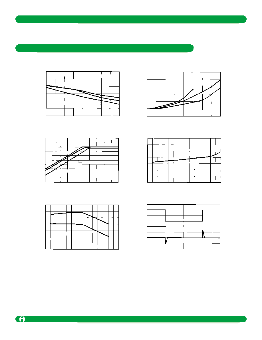
OUTPUT VOLTAGE vs OUTPUT CURRENT
OUTPUT VOLTAGE vs INPUT VOLTAGE
OUTPUT VOLTAGE vs INPUT VOLTAGE
OUTPUT VOLTAGE vs INPUT VOLTAGE
LINE TRANSIENT RESPONSE
V
DO
vs OUTPUT CURRENT
ILC7262CM 3.0V SECTION
ILC7262CM 3.0V SECTION
ILC7262CM 3.0V SECTION
ILC7262CM 3.0V SECTION
ILC7262CM 5.0V SECTION
ILC7262CM 3.0V SECTION
3.1
3.0
2.9
2.8
0 20 40 60 80 100 120 140 160
OUTPUT CURRENT I
OUT
(mA)
OUTPUT VOL
T
AGE V
OUT
(V)
OUTPUT VOL
T
AGE V
OUT
(V)
V
IN
= 4.0V
T
opr
= -30∞C
T
opr
= 25∞C
T
opr
= 25∞C
I
OUT
= 1mA
I
OUT
= 1mA
I
OUT
= 10mA
I
OUT
= 10mA
V
IN
= 4.0V
Input Voltage
Output Voltage
40mA
40mA
10mA
T
opr
= 25∞C
25∞C
80∞C
80∞C
-30∞C
0.6
0.5
0.4
0.3
0.2
0.0
-0.2
V
DO
(V)
0 20 40 60 80 100 120 140 160
OUTPUT CURRENT I
OUT
(mA)
3.2
3.0
2.8
2.6
2.4
2.2
2.5 3.0 3.5
INPUT VOLTAGE V
IN
(V)
T
opr
(∞C)
3.2
3.0
2.8
2.6
2.4
2.2
OUTPUT VOL
T
AGE V
OUT
(V)
3.0 4.0 5.0 6.0 7.0 8.0 9.0 10.0
INPUT VOLTAGE V
IN
(V)
8.0
7.5
7.0
6.5
6.0
5.5
5.0
4.5
4.0
-1 0 1 2 3
TIME (ms)
(V)
OUTPUT VOL
T
AGE V
OUT
(V)
3.01
3.00
2.99
2.98
2.97
2.96
2.95
2.94
-40 -20 0 20 40 60 80 100
Typical Performance Characteristics
General conditions for all curves