
BAR80
Aug-17-2001
1
Silicon RF Switching Diode
Design for use in shunt configuration
High shunt signal isolation
Low shunt insertion loss
4
3
1
2
VSO05553
Type
Marking
Pin Configuration
Package
BAR80
AAs
1 = C
2 = A
3 = C
4 = A
MW-4
Maximum Ratings
Symbol
Value
Unit
Parameter
Diode reverse voltage
V
V
R
35
I
F
100
mA
Forward current
Junction temperature
150
�C
T
j
Operating temperature range
T
op
-55 ... 125
Storage temperature
T
stg
-55 ... 150
BAR80
Aug-17-2001
2
Electrical Characteristics at T
A
= 25�C, unless otherwise specified.
Parameter
Symbol
Values
Unit
min.
typ.
max.
DC characteristics
Reverse current
V
R
= 20 V
I
R
-
-
20
nA
Forward voltage
I
F
= 100 mA
V
F
0.8
-
1
V
AC characteristics
Diode capacitance
V
R
= 1 V, f = 1 MHz
V
R
= 3 V, f = 1 MHz
C
T
-
0.6
1
0.92
1.6
1.3
pF
Forward resistance
I
F
= 5 mA, f = 100 MHz
r
f
-
0.5
0.7
Series inductance chip to ground
L
s
-
0.14
-
nH
Application information
Shunt signal isolation
I
F
= 10 mA, f = 2 GHz, R
G
=R
L
=50
S
I
-
23
-
dB
Shunt insertion loss
V
R
= 5 V, f = 2 GHz, R
G
=R
L
=50
I
L
-
0.15
-
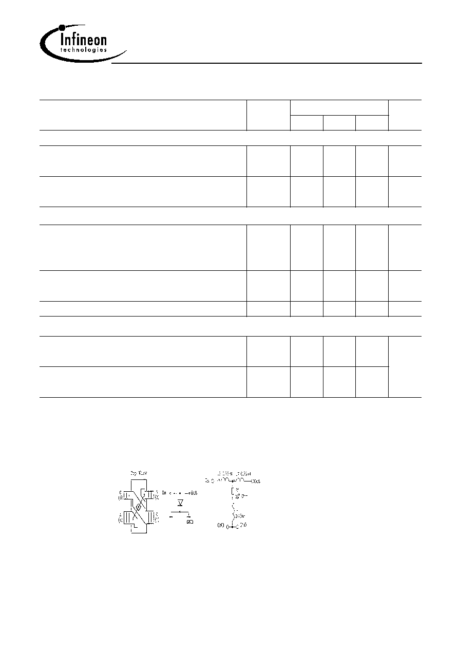
Configuration of the shunt-diode
- A perfect ground is essential for optimum isolation
- The anode pins should be used as passage for RF

