
Aug-06-2001
1
BAS170W
VPS05176
1
2
Silicon Schottky Diode
General-purpose diode for high-speed switching
Circuit protection
Voltage clamping
High-level detection and mixing
Type
Marking
Pin Configuration
Package
BAS170W
7
1 = C
2 = A
-
SOD323
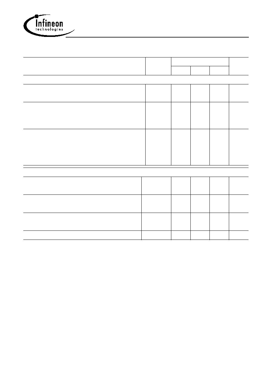
Maximum Ratings
Parameter
Symbol
Value
Unit
Diode reverse voltage
V
R
70
V
Forward current
I
F
70
mA
Surge forward current, t
10 ms
I
FSM
100
Total power dissipation
T
S
= 97 �C
P
tot
250
mW
Junction temperature
T
j
150
�C
Operating temperature range
T
op
-55 ... 125
Storage temperature
T
stg
-55 ... 150
Thermal Resistance
Parameter
Symbol
Value
Unit
Junction - soldering point
1)
R
thJS
190
K/W
1
For calculation of R
thJA
please refer to Application Note Thermal Resistance
Aug-06-2001
2
BAS170W
Electrical Characteristics at T
A
= 25�C, unless otherwise specified
Parameter
Symbol
Values
Unit
min.
typ.
max.
DC Characteristics
Breakdown voltage
I
(BR)
= 10
A
V
(BR)
70
-
-
V
Reverse current
V
R
= 50 V
V
R
= 70 V
I
R
-
-
-
-
0.1
10
�A
Forward voltage
I
F
= 1 mA
I
F
= 10 mA
I
F
= 15 mA
V
F
300
600
750
375
705
880
410
750
1000
mV
AC Characteristics
Diode capacitance-
V
R
= 0 V, f = 1 MHz
C
T
-
1.5
2
pF
Differential forward resistance
I
F
= 5 mA, f = 10 kHz
R
F
-
34
-
Charge carrier life time
I
F
= 25 mA
rr
-
-
100
ps
Series inductance
L
S
-
1.8
-
nH

